Note: Descriptions are shown in the official language in which they were submitted.
CA 02514060 2005-07-21
ALUMINUM MATERIAL HAVING A1N REGION ON THE SURFACE THEREOF
AND METHOD FOR PRODUCTION THEREOF
Technical Field
The present invention relates to a process of
producing a thick aluminum nitride on the surface of an
aluminum material in a short time and to an aluminum
material having a thick aluminum nitride region on the
surface thereof.
Background Art
Conventionally, various methods have been proposed
to develop wear resistance by forming an aluminum nitride
on the surface of an aluminum material or aluminum alloy.
For instance, Japanese Patent Application Laid-Open (JP-A)
No. 60-211061 (Reference 1) discloses a process of
producing an aluminum material having an aluminum nitride
layer, in which the process comprises a step of activating
the surface of a material such as aluminum to be treated
and a step of ion-nitriding the surface to be treated by
glow discharge to form an aluminum nitride layer on the
surface.
Also, JP-A No. 5-179420 (Reference 2) discloses a
method which improves the drawbacks of JP-A No. 60-211061,
i.e., decreased thickness of A1N, unevenness of wear
resistance and insufficient adhesion between A1N and a base
material. Briefly, JP-A No. 5-179420 discloses an aluminum
1
CA 02514060 2005-07-21
material comprising a base material such as aluminum, an
Al-Ag intermetallic compound layer formed on the surface of
the base material and an A1N layer formed on the
intermetallic compound layer, with improved wear
resistance.
However, the Reference 1 could not provide the A1N
layer having sufficient thickness, since the Reference 1
could provide the A1N layer having several tens ~m at most,
which is actually limited to about several Vim, as described
in the Reference 2. Also, it takes longer time, e.g., 24
hours to form the A1N layer having a thickness of several
Nm to several tens Vim, and thus, the method was undesirable
also in view of cost. Since the resultant A1N layer is
uneven, desired wear resistance cannot be obtained. The
A1N layer also has low adhesion to aluminum to be treated,
so that peeling is observed. Therefore, the Reference 1
could not provide desired one in this point of view.
Also, the method of the Reference 2 somewhat
improves the drawbacks of the Reference 1. However, the
method of the Reference 2 has the problem that cracks occur
when the film thickness of AlN exceeds 10 ~m (Reference 2
[0036]). Also, since Ag is used for the intermediate
layer, the method is undesirable in view of cost. Further,
the method of the Reference 2 is limited in selecting
materials as follows: 1) the aluminum material should
contain silver and 2) the intermediate layer containing
silver should be precipitated "film-wise". In addition to
2
CA 02514060 2005-07-21
the limitations, this method also has the problem that the
adhesive strength of the base material, aluminum material
to AlN depends on the intermediate layer, through which AlN
is formed, leading to a loss of selectivity of mechanical
strength.
Disclosure of Invention
An object of the present invention is to solve the
problem possessed by conventional processes of producing an
aluminum material having an AlN layer on the surface
thereof.
Specifically, an object of the present invention is
to provide a process of producing an aluminum material
having a thick A1N region on the surface thereof in a short
time. In particular, other than or in addition to the
above-mentioned objects, an object of the present invention
is to provide a process of producing an aluminum material
having a thick AlN region on the surface thereof, wherein
the A1N region is uniform within the region and has high
adhesion to a base material.
Other than or in addition to the above-mentioned
objects, another object of the present invention is to
provide an aluminum material having a thick AlN region on
the surface thereof, in particular, to provide an aluminum
material having an A1N region on the surface thereof
wherein the A1N region has enhanced film thickness, is
uniform within the region and has high adhesion to a base
3
CA 02514060 2005-07-21
material.
The present inventors have found that CuAl2 is
effective to help the nucleation and growth of A1N. The
present inventors have found that an aluminum material
having an A1N region on a predetermined area of the surface
thereof can be provided by using, as a base material, an
aluminum material containing CuAl2. Specifically, the
present inventors have found the following inventions:
<1> A process of producing an aluminum material
having an aluminum nitride (AlN) region on the surface
thereof, comprising the steps of:
preparing an aluminum material containing CuAl2; and
plasma nitriding the aluminum material, to thereby
form an A1N region on the surface of the aluminum material.
<2> In the above item <1>, the process may further
comprise a step of sputtering the aluminum material to
remove A1203 present on the surface of the aluminum
material prior to the plasma nitriding step.
<3> In the above item <1> or <2>, the plasma
nitriding step may be carried out at -167 to 630°C,
preferably -167 to 550°C, more preferably -167 to 450°C.
<4> In any one of the above items <1> to <3>, the
plasma nitriding step may comprise a treating step which
consists of a step of applying a pulse voltage of -50 V to
-50 kV for 0.1 ~s to 10 ms followed by a application
suspending step having 0.1 ~s to 100 ms; or the plasma
nitriding step may comprise a treating step which comprises
4
CA 02514060 2005-07-21
a step of applying a continuous D.C. voltage of -50 to -800
V, in an activated first nitriding gas atmosphere.
<5> In the above item <4>, the first nitriding
gas may be a gas made from nitrogen and hydrogen and/or a
gas comprising nitrogen gas and hydrogen gas. In the case
where the first nitriding gas is a gas made from nitrogen
and hydrogen, the first nitriding gas may be NH3 or mixed
gas consisting of NH3 and inert gas. In the case where the
first nitriding gas is a gas comprising nitrogen gas and
hydrogen gas, partial pressure of nitrogen gas may be O.OI
to 40 Torr and partial pressure of hydrogen gas may be 0.01
to 100 Torr. More preferably, the first nitriding gas may
have 1:3 of partial pressure ratio of nitrogen gas to
hydrogen gas, and/or may have 1:3 of a molar ratio of
nitrogen to hydrogen (N: H).
<6> In any one of the above items <1> to <5>, AlN
may be produced at a rate of 0.05 ~m/hour or more,
preferably 0.5 to 50 ~m/hour, in the plasma nitriding step.
<7> In any one of the above items <2> to <6>, the
sputtering step may be carried out using the aluminum
material as the negative electrode by applying a D.C.
voltage of -50 V to -4000 V in an atmosphere of chemically
activated second nitriding gas. The second nitriding gas
may be nitrogen, and the partial pressure of nitrogen may
be 0.01 to 20 Torr.
<8> In any one of the above items <1> to <7>,
CuAl2 may be contained in the A1N region of the obtained
CA 02514060 2005-07-21
aluminum material.
<9> An aluminum material having an A1N region on
the surface thereof, wherein the A1N region has CuAl2.
<10> An aluminum material having an AlN region on
the surface thereof, wherein CuAl2 is finely dispersed in
the A1N region.
<11> In the above item <9> or <10>, the A1N region
has a thickness of 0.1 ~m or more, preferably 2 to 2000 Vim,
more preferably 4 to 200 Vim.
<12> In any one of the above items <9> to <11>,
the A1N region may be grown at a rate of 0.05 ~m/hour or
more, preferably 0.5 to 50 ~m/hour.
<13> In any one of the above items <9> to <12>,
the A1N region may have a Vickers hardness (Hv) of 4 GPa or
more, preferably 7 to 15 GPa, more preferably 7 to 14 GPa.
<14> In any one of the above items <9> to <13>,
the A1N region may have a thermal conductivity of 100 W/mK
or more, preferably 100 to 340 W/mK.
<15> In any one of the above items <9> to <14>,
the tensile fracture strength between the A1N region and
the aluminum material may be not less than the tensile
fracture strength of the aluminum material and may be I5
GPa or less, preferably 7 to 11 GPa.
<16> A process of producing an aluminum material
having an aluminum nitride (AlN) region on the surface
thereof, comprising:
a solution treatment step of subjecting an A1 alloy
6
CA 02514060 2005-07-21
containing Cu to a solution treatment at a solution
treatment temperature; and
an age-precipitation step of subjecting the alloy
obtained by the solution treatment step to a heat treatment
at an age-precipitation temperature lower than the solution
treatment temperature, to precipitate CuAl2 and to obtain
an aluminum material having CuAl2; and
a plasma nitriding step of plasma nitriding the
aluminum material, to thereby form an A1N region on the
surface of the aluminum material.
<17> In the above item <16>, the plasma nitriding
step may fill the roles) of one or both of the solution
treatment step and the age-precipitation step, in
particular, the roles) of the age-precipitation step, by
controlling a temperature of the plasma nitriding step.
<18> In the above item <16> or <17>, the process
may further comprise a step of sputtering the aluminum
material to remove A1z03 present on the surface of the
aluminum material prior to the plasma nitriding step.
<19> In the above item <18>, the sputtering step
may fill the roles) of one or both of the solution
treatment step and the age-precipitation step, in
particular, a role of the age-precipitation step, by
controlling a temperature of the sputtering step.
<20> In the above item <18> or <19>, the
temperature of the sputtering step may be lower by at least
10°C, preferably by 10 to 50°C than the solution treatment
7
CA 02514060 2005-07-21
temperature, thereby allowing the precipitation morphology
and distribution of CuAl2 in the age-precipitation step not
to be changed practically.
<21> In any one of the above items <16> to <20>,
the plasma nitriding step may be carried out at -167 to
630°C, preferably -167 to 550°C, more preferably -167 to
450°C.
<22> In any one of the above item <16> to <21>,
the temperature of the plasma nitriding step may be lower
by at least 10°C, preferably by 10 to 50°C than the age-
precipitation temperature, thereby allowing the
precipitation morphology and distribution of CuAl2 in the
age-precipitation step not to be changed practically,
<23> In any one of the above items <16> to <22>,
the plasma nitriding step may comprise a treating step
which consists of a step of applying a pulse voltage of -50
V to -50 kV for 0.1 ~s to 10 ms followed by a application
suspending step having 0.1 ~,s to 100 ms; or the plasma
nitriding step may comprise a treating step which comprises
a step of applying a continuous D.C. voltage of -50 to -800
V, in an activated first nitriding gas atmosphere.
<24> In the above item <23>, the first nitriding
gas may be a gas made from nitrogen and hydrogen and/or a
gas comprising nitrogen gas and hydrogen gas. In the case
where the first nitriding gas is a gas made from nitrogen
and hydrogen, the first nitriding gas may be NH3 or mixed
gas consisting of NH3 and inert gas. In the case where the
8
CA 02514060 2005-07-21
first nitriding gas is a gas comprising nitrogen gas and
hydrogen gas, partial pressure of nitrogen gas may be 0.01
to 40 Torr and partial pressure of hydrogen gas may be 0.01
to 100 Torr. More preferably, the first nitriding gas may
have 1:3 of partial pressure ratio of nitrogen gas to
hydrogen gas, and/or may have 1:3 of a molar ratio of
nitrogen to hydrogen (N: H).
<25> In any one of the above items <16> to <24>,
A1N may be produced at a rate of 0.05 ~,m/hour or more,
preferably 0.5 to 50 ~m/hour, in the plasma nitriding step.
<26> In any one of the above items <18> to <25>,
the sputtering step may be carried out using the aluminum
material as the negative electrode by applying a D.C.
voltage of -50 V to -4000 V in an atmosphere of chemically
activated second nitriding gas. The second nitriding gas
may be nitrogen, and the partial pressure of nitrogen may
be 0.01 to 20 Torr.
<27> In any one of the above items <16> to <26>,
CuAl2 may be contained in the A1N region of the obtained
aluminum material.
Brief Description of the Drawings
Fig. 1 is a SEM image of A1-6Cu showing the presence
o f CuAl2 .
Fig. 2 is a SEM image of A1-6Cu-0.5Mg showing the
presence of CuAl2.
Fig. 3 is a SEM image of A1-6Cu-2Mg showing the
9
CA 02514060 2005-07-21
presence of CuAl2.
Fig. 4 is a graph showing the results of X-ray
diffraction analysis (incident angle: 1°) of B-2
(sputtering time: 0.5 hours) and B-5 (sputtering time: 2
hours) which are prepared using an A1-6Cu-0.5Mg alloy as a
base material.
Fig. 5 is a graph showing the results of X-ray
diffraction analysis (incident angle: 1°) of B-3 prepared
using an A1-6Cu-0.5Mg alloy and B-6 prepared using an Al-
6Cu alloy as a base material.
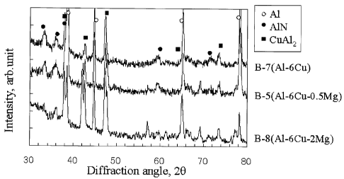
Fig. 6 is a graph showing the results of X-ray
diffraction analysis (incident angle: 1°) of B-5 prepared
using an A1-6Cu-0.5Mg alloy, B-7 prepared using an A1-6Cu
alloy and B-8 prepared using an Al-6Cu-2Mg alloy as a base
material.
Fig. 7 is a graph showing the results of X-ray
diffraction analysis (incident angle: 1°) of B-1 to B-4
(time: 2, 4, 6 and 8 hours) prepared using an A1-6Cu-0.5Mg
alloy as a base material by changing the time required for
plasma nitriding treatment.
Fig. 8 is a sectional SEM image of B-2 (plasma
nitriding treatment time: 4 hours) prepared using an A1-
6Cu-0.5Mg alloy as a base material.
Fig. 9 is a graph showing a sectional SEM image of
B-3 (plasma nitriding treatment time: 6 hours) prepared
using an A1-6Cu-0.5Mg alloy as a base material.
Fig. 10 is a view showing the results of measurement
CA 02514060 2005-07-21
of the hardness (Vickers Hardness) of each section of B-2
and B-3.
Best Mode for Carrying Out the Invention
Hereinafter, the present invention will be described
in detail.
The present invention provides a process of
producing an aluminum material having an aluminum nitride
(A1N) region on the surface thereof, the process comprising
a step of preparing an aluminum material containing CuAl2
and a step of plasma-nitriding the aluminum material to
thereby form an AlN region on the surface of the aluminum
material.
The present inventors have found that the presence
of CuAlz, which helps the nucleation and growth of A1N in
the aluminum material used as a base material, is effective
to form a thick AlN layer in a short time and to form an
A1N layer having high adhesion to the base material.
The aluminum material used as the base material
contains CuAlz. The amount of CuAl2 contained in the
aluminum material (base material) depends on the desired
area of the AlN region on the surface of the aluminum
material, the conditions of plasma nitriding treatment (for
example, treating time and treating temperature) and the
like. The aluminum material used as the base material
preferably contains CuAl2 so that the amount of Cu is 55
mass% or less, preferably 0.5 to 6 masso when the total
11
CA 02514060 2005-07-21
amount of the aluminum material is 100 masso; or the volo
of CuAl2 is 10 volo or less, preferably 0.5 to 6.5 volo
when the total volume of the aluminum material is 100 volo.
As mentioned above, the present inventors have found
that A1N-nucleation and A1N-growth are accommodated by a
helper, CuAl2, Therefore, if CuAl2 which is to help the
AlN-growth, for example, uniformly dispersed in the
aluminum material (base material), A1N can grow on CuAl2
uniformly dispersed as a nucleation site. Therefore, it is
possible to form an AlN layer having uniform thickness on
the entire surface of the aluminum material by carrying out
plasma nitriding treatment for a predetermined time. Also,
CuAl2, nucleation site of A1N, arranged in a straight-line
on the surface of the aluminum material (base material) can
form a linear or band A1N layer (A1N region) on the surface
of the aluminum material.
"A step of preparing an aluminum material containing
CuAl2" involves a step of treating the aluminum base
material so that the aluminum material as the base material
is made to contain CuAl2 when it originally contains no
CuAl2. Examples of the aluminum base material containing
no CuAl2 may include aluminum alloys containing copper and
aluminum alloys containing copper and alloy elements other
than copper. "The step of preparing an aluminum material
containing CuAl2" involves a step of using a commercially
available aluminum alloy containing CuAl2 as it is.
Examples of the aluminum material having CuAl2 may
12
CA 02514060 2005-07-21
include, but are not limited to, Al-6Cu, A1-6Cu-0.5Mg, Al-
6Cu-2Mg, Al-(0.2-55)Cu-(0.05-1)Ti, A1-(0.2-55)Cu-(0.1-
10)Mg-(0.05-1)Ti, and the like. A step of treating an
aluminum base material so as to make the base material
contain CuAl2 allows the aluminum material to be designed
such that CuAl2 is arranged to have various morphology and
distribution as mentioned above.
when the material to be used contains no CuAl2, "the
step of preparing an aluminum material containing CuAlz"
preferably involves the following steps (1) to (4) to
"prepare an aluminum material containing CuAl2": (1) a step
(melting and casting step) of melting and casting an A1
alloy (Al-Cu alloy) containing Cu; (2) a forging and
rolling step; (3) a solution treatment step; and (4) an
age-precipitation step.
Here, the melting and casting step (I) is a step
where a material to be used is a pure A1 or Cu material and
a step of producing an aluminum alloy containing Cu, for
example, an A1-Cu alloy. The forging and rolling step (2)
is a step of forging and/or rolling the resulting A1 alloy.
Also, the solution treatment step (3) is a step of
preparing a supersaturated solid solution at ambient
temperature in the following manner: an A1 alloy is heated
to a temperature (solution treatment temperature) higher
than the melting temperature of elements (for example, Cu
in the case of an A1-Cu alloy) other than A1 to melt the
elements other than Al into a supersaturated solid
13
CA 02514060 2005-07-21
solution, and after the solution treatment step is
sufficiently completed, the solid solution is cooled
rapidly at such a cooling rate not to segregate the
elements other than Al or not to precipitate any crystals
containing these elements. In the case of, for example, an
Al-Cu alloy, the cooling speed in the solution treatment
step is decreased (gradually cooled) whereby the aluminum
material containing CuAl2 can be prepared, without using
the age-precipitation step (4).
The age-precipitation step (4) is a step of
precipitating CuAl2 by keeping a temperature lower than the
solution treatment temperature in the solution treatment
step (3) under heating. Generally, the age-precipitation
step (4) makes it possible to prepare the aluminum material
containing CuAl2. Furthermore, CuAl2 can be precipitated
in the sputtering step and/or the plasma nitriding step, as
described later, by controlling the conditions such as
temperature and/or time in these steps. There is therefore
the case where the sputtering step and/or the plasma
nitriding step as described later may work as the age-
precipitation step, namely, "the step of preparing an
aluminum material having CuAlz".
The aluminum material may be a bulk or powder form.
The powder form used herein means materials ranging from
chip materials having an average particle diameter of about
1 mm to powders having an average particle diameter of 1
Vim. Therefore, the present invention can provide an
14
CA 02514060 2005-07-21
aluminum powder form material having an AlN region in a
predetermined area of the surface thereof and also an
aluminum bulk material having an A1N region in a
predetermined area of the surface thereof.
After the step of preparing an aluminum material,
the aluminum material is subjected to a step of plasma-
nitriding the aluminum material. Prior to the plasma
nitriding, the aluminum material is preferably subjected to
a process of removing A1203 present on the surface of the
aluminum material, for example, a sputtering step.
The process of removing A1203 may use conventional
processes. Examples of the process of removing A1203 may
include, but are not limited to, a reduction using chlorine
ions, argon ion sputtering, and the like. In the present
invention, the process of removing A1203 is preferably
carried out in the following manner because of the
relevance to the plasma nitriding treatment that will be
carried out afterwards: the aluminum material as the base
material is placed in a container, the container is
evacuated, then, a D.C. voltage of -50 V to -4000 V is
applied by using the aluminum material as the negative
electrode under an atmosphere of nitriding gas, preferably
1 Torr nitrogen, to carry out sputtering of the aluminum
material for 1 minute to several hours.
The sputtering step is preferably carried out in the
atmosphere of chemically activated second nitriding gas.
The term "the second nitriding gas" used herein may be only
CA 02514060 2005-07-21
NZ gas or a mixture of Nz gas and an inert gas (for
example, Ar gas).
As mentioned above, there is the case where the
sputtering step may work as "the age-precipitation step",
namely, "the step of preparing an aluminum material having
CuAl2", depending on the conditions such as temperature
and/or time.
Then, the aluminum material is subjected to a plasma
nitriding step. This step ensures that an aluminum nitride
(AlN) region is formed on the surface of the aluminum
material.
The plasma nitriding step is preferably carried out
in the following condition. As to the temperature
condition, the plasma nitriding step is carried out at -167
to 630°C, preferably -167 to 550°C, more preferably -167 to
450°C. Also, as to the conditions other than the above
temperature, the plasma nitriding step, using the aluminum
materials as the negative electrode, includes a treating
step involving an application step of applying a pulse
voltage of -50 to -50 kV, preferably -50 to -1000 V for 0.1
~s to 10 ms, preferably 0.1 ~s to 1 ms followed by the
application suspending step carried out for 0.1 ~s to 100
ms, preferably 10 ~s to 100 ms; or a treating step of
applying a continuous D.C. voltage of -50 to -800 V. In
the case of performing the treating step involving the
application step and the application suspending step, it is
preferable to repeatedly carry out this cycle of the
16
CA 02514060 2005-07-21
application step and application suspending step. The
treating step may be carried out for 0.5 hours or more, for
example, 0.5 to 100 hours, although the treating time
differs depending on the desired thickness of A1N.
As mentioned above, there is the case where the
plasma nitriding step may work as "the age-precipitation
step", namely, "the step of preparing an aluminum material
containing CuAl2", depending on the conditions such as
temperature and/or time.
CuAl2 in the aluminum material is changed in its
precipitation morphology and distribution according to the
temperatures in the sputtering step and/or the plasma
nitriding step. When the temperature in the sputtering
step and/or the plasma nitriding step is either close to
the temperature in the age-precipitation step (4)
(temporarily named as "Tj") or higher than, for example,
more than (Tj -10)°C, CuAl2 in the aluminum material is
changed in its precipitation morphology and distribution.
Therefore, it is not intended to change the precipitation
morphology and distribution of CuAl2 in the aluminum
material in the sputtering step and/or the plasma nitriding
step, the temperature in the sputtering step and/or the
plasma nitriding step is a temperature lower by at least
10°C ((Tj - 10)°C or less), preferably a temperature lower
by 10 to 50°C ((Tj - 10) to (Tj - 50)°C) than that in the
age-precipitation step (4). On the other hand, in the case
where CuAl2 in the aluminum material is allowed to be
17
CA 02514060 2005-07-21
changed in the precipitation morphology and distribution,
it is possible to select a temperature depending on the
desired precipitation morphology and distribution.
Also, the atmosphere in the plasma nitriding step is
preferably the first nitriding gas atmosphere. Here, the
first nitriding gas may be a gas made from nitrogen and
hydrogen, and/or a gas comprising nitrogen gas and hydrogen
gas. The term "a gas made from nitrogen and hydrogen"
means a gas made from an element N and an element H such as
NH3 gas. The term "a gas having a gas comprising nitrogen
and hydrogen" means a mixture gas of NH3 gas and, for
example, an inert gas (e.g., Ar gas). Also, the term "a
gas consisting of nitrogen gas and hydrogen gas" may be a
gas comprising only Hz gas and N2 gas or a gas further
comprising, for example, an inert gas (for example, Ar
gas). "The gas having a gas comprising nitrogen and
hydrogen" is preferably NH3 gas or a mixture gas of NH3 gas
and Ar gas. "The gas comprising nitrogen gas and hydrogen
gas" is preferably a gas comprising a nitrogen gas partial
pressure of 0.01 to 40 Torr and a hydrogen gas partial
pressure of 0.01 to 100 Torr. The first nitriding gas may
be a gas having, for example, NH3 gas, H2 gas and Nz gas.
The first nitriding gas is preferably one in which the
partial pressure ratio of nitrogen gas to hydrogen gas is
1:3 or the molar ratio of nitrogen to hydrogen is 1:3.
The plasma nitriding step in the present invention
can produce AlN at a rate of 0.05 Nm/hour or more,
18
CA 02514060 2005-07-21
preferably 0.5 to 100 ~m/hour.
In particular, the rate of the formation of A1N is
to 13 ~m/hour in the initial stage of the plasma
nitriding step (until four hours from the start of the
nitriding step) and 10 to 30 N,m/hour in the next stage (4
to 6 hours after the nitriding step).
According to the above method, the present invention
can provide an aluminum material having an A1N region on
the surface thereof.
The thickness of the AlN region can be controlled by
changing various parameters in the aforementioned method,
in particular, by changing the parameters in the plasma
nitriding step, for example, plasma nitriding time. For
example, the thickness of the A1N region may be designed to
be 0.01 um or more, for example, 2 to 2000 Vim, preferably 4
to 200 Vim.
The aluminum material obtained by the present
invention has an AlN region on the surface thereof. The
A1N region contains CuAl2. CuAl2 may be present in the AlN
region in columnar structure perpendicular to the surface
of the aluminum material which is the base material, and/or
in fine particles, and/or in film structure at the
interface between the formed AIN region and the surface of
the aluminum material which is the base material. The
morphology of CuAl2 depends on the condition of the
formation of AlN, particularly temperature condition. It
is considered that the presence of CuAl2 makes it possible
19
CA 02514060 2005-07-21
to promote the growth and formation of A1N.
A material in which CuAl2 is formed film-wise on the
interface between the formed AlN region and the surface of
the aluminum material which is the base material, namely, a
material provided with the aluminum material layer, CuAl2
layer and AlN layer which are formed in this order may be
used as a heat sink. A1N is an electrical insulator but it
has superior thermal conductivity, CuAl2 and the aluminum
material in the inside have high strength and excellent
thermal conductivity, and therefore, the material obtained
by combining these layers can be used as a heat sink.
Also, the present invention can provide an aluminum
material provided with the AlN region having a Vickers
hardness (Hv) of 4 GPa or more, preferably 8 to 15 GPa. In
particular, the aluminum material obtained by the present
invention has a thick A1N region and therefore, not only
the surface of AlN but also the Vickers hardness of the
section of A1N can be measured.
The A1N region obtained by the present invention has
high adhesion to the aluminum material which is the base
material. For example, the tensile fracture strength
between the AlN region and the aluminum material which is
the base material is not less than the tensile fracture
strength of the aluminum material, and is 15 GPa or less,
preferably 8 to 11 GPa. The phrase "the tensile fracture
strength between the AlN region and the aluminum material
which is the base material" used herein means, unless
CA 02514060 2005-07-21
stated otherwise, a difference between the Vickers hardness
(Hv) of the aluminum material which is the base material
and the Vickers hardness (Hv) of the AlN region and
indicates the strength necessary to peel the AlN region
from the aluminum material which is the base material.
Because A1N has a thermal conductivity of 100 to 340
W/mK, the aluminum material obtained by the present
invention may be applied as a radiating plate having an AlN
region in a predetermined area.
Also, the aluminum material obtained in the present
invention and having an AlN region on the surface thereof
may be applied to materials used for sliding mechanical
parts, automobile engine parts, trial molds for plastic
forming, heat sinks for semiconductors and the like.
Examples
The present invention will be explained in more
detail by way of examples, which are not intended to be
limiting of the present invention.
Example 1:
Aluminum alloys A-1 to A-3 shown in Table 1 were
respectively prepared in an amount of about 1.3 g
(dimension: about 10 mm (thickness) x about 8 mm x about 6
mm) as a base material. Before these aluminum alloys were
subjected to the treatment as described later, each SEM
image of these aluminum alloys A-1 to A-3 were observed.
As a result, CuAl2 was confirmed in all of these aluminum
21
CA 02514060 2005-07-21
alloys as shown in Figs. 1 to 3.
Table 1.
Aluminum alloy Composition
A-1 Al-6Cu
A-2 A1-6Cu-0.5Mg
A-3 A1-6Cu-2Mg
Each aluminum alloy was disposed in a sealed
container and the container was evacuated. Then, the
surface of the aluminum alloy was subjected to a sputtering
step carried out at 400°C under a 1 torr nitrogen
atmosphere. The condition of the sputtering step was as
follows: an aluminum alloy was used as the negative
electrode, D.C. voltage: -250 to -270 V; 0.1 to 0.2 A;
time: 0.5 hours or 2 hours. Thereafter, the aluminum alloy
was used as a negative electrode to carry out plasma
nitriding treatment under a 1 torr nitrogen (NZ) and 3 torr
hydrogen (H2) atmosphere for 2 hours, 4 hours, 6 hours and
8 hours in the following condition: pulse voltage: -200 V;
0.2 A; and 673 K, thereby obtaining aluminum alloys B-1 to
B-8 having an aluminum nitride (A1N) layer on the surface
thereof. Furthermore, the pulse voltage was applied
repeatedly in the following manner: application: 16 ms and
suspension of application: 32 ms. With regard to these
aluminum alloys B-1 to B-8, the composition of the base
material to be used, and sputtering time and plasma
nitriding time to be used are shown in Table 2.
22
CA 02514060 2005-07-21
Table 2.
Base Sputtering Plasma Remarks
material time (h) nitriding
time (h)
B-1 Al-6Cu-0.5Mg 0.5 2 Fig. 7
B-2 A1-6Cu-0.5Mg 0.5 4 Figs. 4 &
7
B-3 A1-6Cu-0.5Mg 0.5 6 Figs. 5 &
7
B-4 Al-6Cu-0.5Mg 0.5 8 Fig. 7
B-5 A1-6Cu-0.5Mg 2 4 Fig. 4
B-6 A1-6Cu 0.5 6 Fig. 5
B-7 Al-6Cu 2 4 Fig. 6
B-8 Al-6Cu-2Mg 2 4 Fig. 6
Fig. 4 is a graph showing the results of X-ray
diffraction analysis (incident angle: 1°) of B-2
(sputtering time: 0.5 hours) and B-5 (sputtering time: 2
hours) which are prepared using an Al-6Cu-0.5Mg alloy as a
base material. In both of B-2 and B-5, the presence of A1N
was confirmed. It is found from the results that even if
the time of the sputtering, which is pretreatment for
removing A1203, is short, AlN can be formed on the surface
of the aluminum material.
Fig. 5 is a graph showing the results of X-ray
diffraction analysis (incident angle: 1°) of B-6 (Al-6Cu)
and B-3 (Al-6Cu-0.5Mg) which are prepared using an A1-6Cu
alloy or an Al-6Cu-0.5Mg alloy as a base material. The
presence of AlN was confirmed in both B-3 and B-6.
23
CA 02514060 2005-07-21
Fig. 6 is a graph showing the results of X-ray
diffraction analysis (incident angle: 1°) of B-7 (Al-6Cu),
B-5 (A1-6Cu-0.5Mg) and B-8 (A1-6Cu-2Mg) prepared using an
A1-6Cu alloy, an Al-6Cu-0.5Mg alloy or an Al-6Cu-2Mg alloy
as a base material. The presence of A1N was confirmed in
any of B-5, B-7 and B-8.
Fig. 5 and Fig. 6 show that a material having AlN on
the surface thereof can be prepared by using aluminum or an
aluminum alloy in which CuAl2 is present.
Fig. 7 is a graph showing the results of X-ray
diffraction analysis (incident angle: 1°) of B-1 to B-4
prepared using an Al-6Cu-0.5Mg alloy as a base material by
changing the time required for plasma nitriding treatment
to 2 hours, 4 hours, 6 hours and 8 hours. Fig. 7 shows
that when the treating time is longer, the peak of A1 is
relatively smaller and the peak of AlN is relatively
larger, suggesting that A1N is formed on the surface of the
base material. Also, the peak of CuAlz is confirmed at any
time during treating, suggesting that CuAl2 is present on
the surface of base material or in its vicinity regardless
of the plasma nitriding time and that the above CuAl2
promotes the formation of A1N.
Fig. 8 and Fig. 9 show sectional SEM images of B-2
and B-3. Fig. 10 shows the results of measurement of the
hardness (Vickers Hardness) of each section of B-2 and B-3.
In Fig. 10, the abscissa is a distance (um) from the
surface of B-2 or B-3 and the ordinate is Vickers hardness
24
CA 02514060 2005-07-21
(unit: GPa).
Figs. 8, 9 and 10 show that the thickness of the A1N
layer in B-2 (nitriding time: 4 hours) is about 40 ~m and
the thickness of the A1N layer in B-3 (nitriding time: 6
hours) is about 80 Vim. Figs. 8 and 9 also show that the
base material is adhesive to the A1N layer. Further, white
regions are observed in the A1N layer in Figs. 8 and 9.
These white regions are confirmed to be CuAl2 by energy
dispersion type X-ray analysis.
Accordingly, a highly adhesive and thick A1N layer
is formed on the surface of the aluminum alloy in a short
time by way of the present examples. It is also considered
that the presence of CuAl2 promotes the formation of AlN.