Note: Descriptions are shown in the official language in which they were submitted.
CA 02514228 2005-07-25
DESCRIPTION
DISCRIMINATION SENSOR
Technical Field
The present invention relates to a discrimination
sensor having a function of discriminating an object
at a high level.
Background Art
Hitherto, as disclosed in Japanese Patent No.
2896288 (see paragraphs 0007-0009) , there has been known
a discrimination sensor configured to recognize a
surface structure of an object (for example, a complex
pattern applied to the surface of a bill, an integrated
circuit or the like) and also adapted to determine the
authenticity, the accuracy and the like of the object.
Usually, the discrimination sensor of this kind is
disposed at a position corresponding to a characteristic
part of the surface structure (or the pattern) , which
best reflects the characteristic of the object. The
object and the discrimination sensor are made to perform
relative movement. This causes the discrimination
sensor to scan along the characteristic part of the
surface structure. Then, sensing data obtained during
1
CA 02514228 2005-07-25
the scan (that is, data plotted corresponding to the
characteristic part of the surface structure) is
compared with original data. Consequently, the
authenticity, the accuracy and the like of the obj ect
are determined.
Meanwhile, the complex patterns of, for example,
mass-produced bills, integrated circuits or the like
are not applied to exactly the same position on the
surface of each of the objects in such a way as to have
the same shape. During the pattern is printed, a slight
displacement, deformation or the like is caused by the
influenceofprintingprecision and machiningaccuracy.
The conventional discrimination sensor is caused to scan
in a pinspot condition in which a sensing area is
extremely narrow. Even when a slight displacement or
deformation of the pattern of the characteristic part
occurs, sensing data obtained from the characteristic
part largely varies.
More specifically, the discrimination sensor is
fixedly positioned at a certain position. Thus, the
position of the discrimination sensor is not adjusted
according to the displacement, the deformation or the
like of the pattern applied to the surface of the object.
At all times, sensing data obtained from the pattern
corresponding to a specific scanning line is plotted.
2
CA 02514228 2005-07-25
Therefore, for instance, in a case where no displacement,
deformation or the like of the pattern occurs, the
sensing data obtained from the pattern corresponding
to the specific scanning line is always matched with
the original data. In contrast with this, even when
a slight displacement, deformation or the like of the
pattern applied to the specific scanning line occurs,
sensing data obtained by the discrimination sensor
becomes different from original data, regardless of the
fact that the discrimination sensor scans the same
scanning line. This is because of the facts that the
conventional discrimination sensor is in the pinspot
condition in which the sensing area is extremely narrow,
and that when a slight displacement or deformation of
the pattern occurs, the pattern of the characteristic
part is off the sensing area. In this case, the
discrimination sensor is in the same state as if this
sensor scanned a different pattern part. The sensing
data obtained from the different pattern part is compared
withtheoriginaldata. Consequently, theconventional
discrimination sensor has the following problems. For
example, in the case of determining the authenticity
of a bill, a genuine bill is erroneously determined to
be a forged bill . In the case of determining the accuracy
of an integrated circuit, a completed product is
3
CA 02514228 2005-07-25
erroneously determined to be a defective product.
Disclosure of Invention
The invention is accomplished to solve such problems .
One of objects of the invention is to provide a
discrimination sensor having an excellent
discriminating function, which is enabled to determine
the authenticity, the accuracy and the like of an obj ect
correctly or accurately without being affected by a
displacement, deformation or the like of a surface
structure of the object.
According to the invention, there is provided a
discrimination sensor 2 that optically detects a surface
structure 6 of an object 4 by scanning along a surface
of the object 4 in a scanning direction S1. The
discriminationsensorincludes:alightemittingdevice
8 that emits sensing light L to the surface of the object
4, the sensing light L having a sensing area El being
wide in a direction perpendicular to the scanning
direction S1; and a light receiving device 10 having
a light receiving area E2 that receives light R generated
on the surface structure 6 of the object 4 when the sensing
light L is emitted, the light receiving area E2
configured to be wide in a direction perpendicular to
the scanning direction Sl. In the invention, the light
9
CA 02514228 2005-07-25
emitting device may be configured to be able to
individually emit plural sensing light beams (e.g., a
near infrared light beam and a visible light beam) of
wavelength bands differing from each other. The light
receiving device is configured to be able to receive
light beams generated on the surface structure of the
object independently when the sensing light beams of
wavelength bands differing from each other are
individually emitted from the light emitting device.
Further, the discrimination sensor may be provided with
a computation/determination unit 12 adapted to perform
a computation on a discrimination signal outputted from
the light receiving device when receiving light
generated on the surface structure of the obj ect, and
also adapted to determine whether or not a value
represented by the discrimination signal is within a
predetermined tolerance range.
According to the discrimination sensor, during the
surface structure of the object is scanned, plural
sensing light beams of wavelength bands differing from
each other are individually emitted from the light
emitting device. Light beams generated on the surface
structure of the object at that time are converted by
the light receiving device into a discrimination signal,
which istheninputtedtothecomputation/determination
CA 02514228 2005-07-25
unit. Subsequently, the computation/determination
unit determines whether or not a value represented by
the discrimination signal is within a tolerance range.
According to the invention, there is provided a
discrimination sensor that optically detects a surface
structure 6 of an object 4 by scanning along a surface
of the object 4 in a scanning direction S1. The
discrimination sensor includes : a sensor unit 14 having
an optical path opening 14a widely opened in a direction
perpendicular to the scanning direction S1; a light
emitter ( for example 8a' , 8b' ) that is provided in the
sensor unit 14 and emits light; a light receiver 10 that
is provided in the sensor unit 14 and receives light;
and a focusing optical system (for example, 16a, 16b,
16c) that focuses the light emitted from the light
emitter towards the optical path opening 14a, and focuses
light that is incident into the sensor unit 14 through
the optical path opening 19a to the light receiver 10.
According to such a discrimination sensor, a light
beam emitted from the light emitter is focused by the
focusing optical system to the optical path opening.
Thereafter, the focused sensing light beams, the sensing
area corresponding to each of which is wide in a direction
perpendicular to a scanning direction, are focused on
the surface of the object from the optical path opening.
6
CA 02514228 2005-07-25
Then, light beams, which come from the surface structure
of the object and are incident into the sensor unit
through the optical path opening, are focused by the
focusing optical system on the light receiver.
Brief Description of Drawings
In the accompanying drawings:
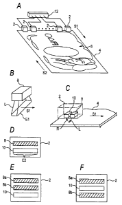
FIG. 1A is a perspective view illustrating a state
of use of a discrimination sensor according to the
embodiment;
FIG. 1B is a perspective view illustrating a state
in which sensing light is emitted from a light emitting
device of the discrimination sensor according to a first
embodiment by assuring a wide sensing area;
FIG. 1C is a perspective view illustrating a state
in which the discrimination sensor moves along a scanning
direction;
FIG. 1D is a plan view illustrating the
discrimination sensor in which the light emitting device
and a light receiving device are formed integrally with
each other;
FIGS. 1E and 1F are plan views each illustrating
a modification of the discrimination sensor in a state
in which the light emitting device is constituted by
two light emitting portions;
7
CA 02514228 2005-07-25
FIG. 2A is a view illustrating a tolerance range
of sample data stored in a computation/determination
unit of the discrimination sensor;
FIG. 2B is a perspective view illustrating a
modification employing a semiconductor substrate on
which a fine integrated circuit is pattern-printed;
FIGS. 2C and 2D are views each illustrating the
configuration of the discrimination sensor in the case
of using transmitted light;
FIG. 3A is a perspective view illustrating the
configuration of a discrimination sensor according to
a second embodiment;
FIGS. 3B to 3E are cross-sectional views, taken
along line IIb-IIb shown in FIG. 3A, illustrating a
sequence of scanning states in which light emitted from
each of light emitters is focused by a focusing optical
system from an optical path opening on an object, and
in which light impinging upon the optical path opening
from the object is focused on a light receiver by the
focusing optical system.
FIG. 4 is a cross-sectional view, taken along line
IV-IV shown in FIG. 3A, illustrating a state in which
light impinging upon the optical path opening from the
object is focused on a light receiver by the focusing
optical system (a focusing lens portion);
8
CA 02514228 2005-07-25
FIGS. 5A and 5B are views illustrating a
modification of the discrimination sensor and also
illustrating a state in which light emitted from a single
light emitting portion is focused by a focusing optical
system from an optical path opening on an object, and
in which light impinging upon the optical path opening
from the obj ect is focused on a light receiver by the
focusing optical system; and
FIGS. 6A and 6B are views illustrating the
configuration of a discrimination sensor in the case
of using transmitted light.
In the figures, reference character 2 designates
a discrimination sensor, reference character 4
designates an object, reference character 6 designates
a surface structure, reference character 8 designates
a light emitting device, reference character 10
designates a light receiving device, reference
character El designates a sensing area, reference
character E2 designates a light receiving area,
reference character L designates sensing light,
reference character R designates light generated on the
surface structure, and reference character S1
designates a scanning direction.
Best Mode for Carrying Out the Invention
9
CA 02514228 2005-07-25
Hereinafter, a discrimination sensor according to
the invention is described with reference to the
accompanying drawings.
As shown in FIG. 1A, a discrimination sensor 2
according to the invention is enabled to optically detect
a surface structure 6 of an obj ect 4 by scanning along
a surface of the object 4. In the description of each
of the following embodiments, a bill (paper money) is
employed as the object 4. A design of characters and
figures printed on a surface of the bill 4 is adopted
as the surface structure 6.
The discrimination sensors 2 are disposed at plural
places in such a way as to be able to sense the surface
structure by scanning along a characteristic part of
the bill 4 serving as an obj ect . FIG. 1A shows an
apparatus configured so that plural discrimination
sensors 2 are arranged at predetermined intervals along
a transversal direction crossing the longitudinal
direction of a bill 9, and scan in the longitudinal
direction of the bill 9 to thereby sense the surface
structure. Alternatively, the apparatus may be
configured so that plural discrimination sensors 2 are
disposed at predetermined intervals along the
longitudinal direction of the bill 4 and scan in the
transverse direction thereof to thereby sense the
CA 02514228 2005-07-25
surface structure. The arrangement intervals and the
number of the discrimination sensors 2 are optionally
set according to the shape and the position of the
characteristic part of the bill 4. Therefore, the
arrangement intervals and the number of the
discrimination sensors 2 are not limited to specific
values. Further, a part, which is effective in
specifying or identifying an object (that is, the bill
4) , is designated as the characteristic part of the bill
4, which is the object.
Furthermore, a method of moving each of the
discrimination sensors 2 in a scanning direction
designated by an arrow S2, and a method of moving the
bill 4 in a scanning direction designated by an arrow
S2 are considered as a method of causing the plural
discrimination sensors 2 to scan along the
characteristic part of the bill 4. In the description
of each of the following embodiments, the method of
moving each of the discrimination sensors 2 in the
scanning direction S1 (see FIG. 1C) is employed by way
of example. Incidentally, in any such method, existing
moving devices can be utilized as means for moving the
discrimination sensors 2 and the bill 4. Thus, the
description of such means is omitted herein. In this
case, a method of controlling movement timings, with
11
CA 02514228 2005-07-25
which the discrimination sensors 2 are respectively
moved, in such a way as to simultaneously move the
discrimination sensors 2 is commonly used. However,
the method of moving the discrimination sensors 2 is
not limited thereto . The apparatus may employ a method
of moving the discrimination sensors 2 by individually
controlling and shifting the movement timings thereof
in such a way as to relatively differ from one another.
FIGS. 1B and 1C show the configuration of the
discrimination sensor 2 according to the first
embodiment of the invention. Such a discrimination
sensor 2 includes a light emitting device 8 adapted to
emit sensing light L, the sensing area E1 corresponding
to which extends in a direction perpendicular to the
scanning direction Sl is wide, toward the surface of
the object (or bill) 4, and also includes a light
receiving device 10 adapted to receive light R generated
on the surface structure 6 of the bill 4 when the sensing
light L is emitted, and also adapted to assure a wide
light receiving area E2 in a direction perpendicular
to the scanning direction S1 . The light emitting device
8 and the light receiving device 10 are formed integrally
with each other in the discrimination sensor 2 (see FIG.
1D) .
In the first embodiment, the light R generated on
12
CA 02514228 2005-07-25
the surface structure 6 of the bill 4 is assumed to be
reflection light reflected from the surface of the bill
4 when the sensing light L is emitted. The reflection
light has optical properties (change in optical power,
scattering, change in wavelength, and the like) , which
vary according to the shape and the position of the
surface structure 6, or to the kind (for example,
magnetic ink) and the shades of ink used for printing
the surface structure 6.
The light emitting device 8 is configured to be able
to individually emit plural sensing light beams L of
wavelength bands differing from each other. The light
receiving device 10 is configured to be able to
sequentially receive light beams R generated on the
surface structure 6 of the bill 4 when the sensing light
beams L of wavelength bands differing from each other
are individually emitted from the light emitting device
8. Incidentally, for example, a method of changing the
oscillating frequency of the light emitting device 8
by changing the value of a voltage applied to the light
emitting device 8 is employed as a method of causing
the light emitting device 8 to individually emit plural
sensing light beams L of wavelength bands differing from
each other.
In this case, it is preferable that one of the sensing
13
CA 02514228 2005-07-25
light beams L of wavelength bands differing from each
other is set in the band of wavelengths from
substantially 700 nm to substantially 1600 nm, and that
the other sensing light beam L is set in the band of
wavelengths from substantially 380 nm to substantially
700 nm. More preferably, one of the sensing light beams
L of wavelength bands differing from each other is set
in the band of wavelengths from substantially 800 nm
to substantially 1000 nm, while the other sensing light
beam L is set in the band of wavelengths from
substantially 550 nm to substantially 650 nm.
Incidentally, in this embodiment, one of the sensing
light beams L of wavelength bands differing from each
other is set in the band of a wavelength of substantially
940 nm, while the other sensing light beam L is set in
the band of a wavelength of substantially 640 nm, by
way of example. Incidentally, for convenience of
description, the sensing light beam L of the band of
wavelengths from substantially 700 nm to substantially
1600 nm is referred to as a near infrared light beam.
The sensing light beam L of the band of wavelengths from
substantially 700 nm to substantially 1600 nm is referred
to as a near infrared light beam. The sensing light
beam L of the band of wavelengths from substantially
380 nm to substantially 700 nm is referred to as a visible
19
CA 02514228 2005-07-25
light beam.
For example, a light-emitting diode (LED), a
semiconductor laser or the like can be employed as the
light emitting device 8 configured to realize light beams
of such wavelength bands . However, as long as the light
beams of the aforementioned wavelength bands can be
realized, other kinds of light emitting devices may be
used as the light emitting device 8.
Preferably, for instance, a method of alternately
emitting a near infrared light beam and a visible light
beam with predetermined timings is employed as a method
of causing the light emitting device 8 to emit sensing
light beams L (that is, a near infrared light beam and
a visible light beam) of wavelength bands differing from
each other. In this case, the timing with which each
of the near infrared light beam and the visible light
beam is emitted, is optionally set according to the
moving speed of each of the discrimination sensors 2,
and to the kind of the object (or the bill) 4. Thus,
the timing is not limited to a specific timing. In this
embodiment, the near infrared light beam and the visible
light beam are alternately emitted with the
predetermined timing . However, as long as the surface
structure 6 of the object (or the bill) 4 can optically
be sensed, other methods may be employed.
CA 02514228 2005-07-25
According to the aforementioned discrimination
sensors 2, during each of the discrimination sensors
2 is moved along the scanning direction S1, the light
emitting device 8 alternately emits a near infrared light
beam and a visible light beam with the predetermined
timing. At that time, the light receiving device 10
sequentially receives light beams R generated on the
surface structure 6 of the bill 4 and outputs an
electrical signal representing a voltage value (or an
electric current value) corresponding to an amount of
the received light beam, that is, a discrimination
signal.
The discrimination sensor 2 has a
computation/determination unit 12. Thus, a
predetermined computation is performed on the
discrimination signal, which is outputted from the light
receiving device 10, in the computation/determination
unit 12. Then, it is determined whether or not the value
represented by the discrimination signal is within a
predetermined tolerance range.
Preliminarily detected sample data is stored in the
computation/determination unit 12. The sample data is
constituted by data that is obtained by optically sensing
the surface structure of a sample object (a genuine bill
in a case where the object to be scanned is a bill) of
16
CA 02514228 2005-07-25
the same kind as the kind of an obj ect (or bill ) 4 scanned
by the discrimination sensor 2. Practically, many (for
example, hundreds of) sample objects are prepared.
Then, sensing data respectively obtained from the sample
obj ects are detected. The sample data obtained at that
time is detected as data, which represents a value having
a certain range as shown in, for example, FIG. 2A, due
to a displacement, deformation or the like of the surface
structure. Incidentally, such sample data includes
values represented by electrical signals (or digital
signals) outputted from the light receiving device 10,
all of which are plotted. In this case, a region between
a "maximum line" M1, which connects points that
correspond to maximum values represented by the sample
data, and a "minimum line" M2, which connects points
that correspond to minimum values represented by the
sample data, is defined herein as a tolerance range.
It is determined according to a computation
performed by the computation/determination unit 12
whether or not a value represented by the discrimination
signal outputted from the light receiving device 10 is
within the range defined between the "maximum line" M1
and the "minimum line" M2. Practically, when the bill
9, which is the object, is genuine, the values
represented by the discrimination signals outputted
17
CA 02514228 2005-07-25
from the light receiving device 10 are plotted along
the region (that is, the tolerance range) defined between
the "maximum line" M1 and the "minimum line" M2. In
contrast with this, when the value represented by the
discrimination signal outputted from the light
receiving device 10 is out of the tolerance range, it
is determined that the bill 4 is a forged bill. In this
case, the reflection light R generated on the surface
structure 6 of a new bill 4 differs in optical property
(or light quantity) from that generated on the surface
structure 6 of an old bill 4. However, the light quantity
of the reflection light R (thus, the signal strength
of the discrimination signal) differs only slightly
between the new bill and the old bill. Thus, there is
no need for setting the range between the "maximum line"
M1 and the "minimum line" M2, which are obtained from
the preliminarily detected sample data, at a large value.
Consequently, determination accuracy can be enhanced.
As described above, in accordance with the
discrimination sensor 2 according to the first
embodiment, the authenticity of the object can be
determined correctly without being affected by a
displacement, deformation or the like of the surface
structure of the object (the bill, in the embodiment)
by employing the sensing light adapted so that the
18
CA 02514228 2005-07-25
corresponding wide sensing area extending in a direction
perpendicular to the scanning direction is assured.
Also, the surface structure 6 of the object can be
determined with high-level discrimination ability by
sensing the surface structure by individually emitting
plural sensing light beams L of wavelength bands
differing from each other.
Incidentally, although the bill 4 is employed as
the object in the aforementioned embodiment, the object
is not limited thereto. For instance, as shown in FIG.
2B, a semiconductor substrate, onwhich a fine integrated
circuit is pattern-printed, maybe employed as the objectw
4. The surface structure 6 in this case is the
pattern-printed integrated circuit. With such a
configuration, the accuracy of the integrated circuit
6 can be determined. Thus, the yield of products can
be enhanced.
Further, althoughthe aforementionedembodiment is
configured so that the light emitting device 8 singly
and individually emits sensing light beams (that is,
a near infrared light beam and a visible light beam)
L of wavelength bands differing from each other (with
the predetermined timing alternately). The light
emitting device according to the invention is not limited
thereto . For example, as shown in FIGS . 1E and 1F, the
19
CA 02514228 2005-07-25
light emitting device 8 may be constituted by plural
(or two) light emitting portions 8a and 8b each adapted
to individually emit sensing light beams (that is, a
near infrared light beam and a visible light beam) L
of wavelength bands differing from each other. For
instance, one of the light emitting portions 8a emits
a near infrared light beam, while the other light
emitting portion 8b emits a visible light beam.
Although an example of the discrimination sensor
2 using the reflection light R has been described in
the description of the embodiment, the discrimination
sensor 2 according to the invention is not limited
thereto . For example, as shown in FIGS . 2C and 2D, the
discrimination sensor 2 using transmitted light may be
employed. In this case, paired discrimination sensors
2 are disposed across the obj ect 4 in such a way as to
be opposed to each other. The light receiving function
of the light receiving device 10 of one of the
discrimination sensors 2 is stopped. The light
emitting function of the light emitting device 8 (thus,
each of the light emitting portions 8a and 8b) of the
otherdiscriminationsensor2isstopped. Consequently,
sensing light beams (that is, a near infrared beam and
a visible light beam) emitted from the light emitting
device 8 (thus, each of the light emitting portions 8a
CA 02514228 2005-07-25
and 8b) of one of the discrimination sensors 2 are
transmitted by the object 4. Thereafter, the
transmitted light beams are received by the light
receiving device 10 of the other discrimination sensor
2. Incidentally, in the case of using the
discrimination sensor 2 of the transmission type, the
object 4 is limited to those having optical transparency.
Next, a discrimination sensor according to a second
embodiment of the invention is described hereinbelow
with reference to the accompanying drawings. In the
aforementioned first embodiment, the light emitting
device 8 is configured to have a wide rectangular shape
so as to emit sensing light beams L, the sensing area
E1 corresponding to each of which extends in a direction
perpendicular to the scanning direction S1 and is assured
to be wide. The light receiving area E2 of the light
receiving device 10 is assured in such a way as to be
wide in a direction perpendicular to the scanning
direction S1 so as to receive light R generated on the
surface structure 6 of the bill 9 when such sensing light
beams L are emitted . In contrast with this, in the second
embodiment, commerciallyavailable light emitters (8a'
and 8b' ) and commercially available light receivers 10'
are used, as will be described later. Light beams
radially emitted from each of the light emitters (8a'
21
CA 02514228 2005-07-25
and 8b' ) are set by a focusing optical system (16a and
16b) to be the sensing light beams L, the sensing area
E1 corresponding to each of which is assured to be wide
in a direction perpendicular to the scanning direction
S1. Light R generated on the surface structure 6 of
the bill 4 is focused on the light receiver 10' by the
focusing optical system (16c).
As shown in FIGS . 3A to 3E, the discrimination sensor
2 according to this embodiment is provided with a sensor
unit 14 having an optical path opening 14a widely opened
in a direction perpendicular to the scanning direction
S1. In the sensor unit 14, light emitters (for example,
8a' and 8b' ) each adapted to emit predetermined light,
and a focusing optical system ( for instance, 16a, 16b,
and 16c) formed integrally with the sensor unit 14 are
provided. The focusing optical system (16a, 16b, and
16c) focuses light emitted from the light emitters (8a'
and 8b' ) toward the optical path opening 14a and also
focuses light, which is incident into the sensor unit
19 through the optical path opening 19a, toward the light
receiver 10'.
In this case, the light emitted from the light beams
emitters (8a' and 8b') are focused by the focusing
optical system (16a, 16b, and 16c) to the optical path
opening 14a. Thereafter, the focused light beams are
22
CA 02514228 2005-07-25
used as the sensing light beams (L1, L2), the
corresponding sensing area (for example, the sensing
area designated by reference character E1 shown in FIG.
1B) of each of which is assured in such a way as to be
wide in a direction perpendicular to the scanning
direction Sl. The sensing light is focused on the
surface of the object (the bill, in the embodiment) 4
from the optical path opening 14a. Light beams (R1,
R2) generated on the surface structure 6 (see FIG. 1A)
of the bill 4 are incident into the sensor unit 14 through
the optical path opening 14a. Subsequently, the
incident light beams are focused by the focusing optical
system (16a, 16b, and 16c) onto the light receiver 10' .
In the embodiment, the predetermined light beams
emitted from the light emitters (8a' and 8b' ) is assumed
to be sensing light beams (that is, a near infrared light
beam L1 and a visible light beam L2 (to be described
later) ) of wavelength bands differing from each other.
Further, the predetermined light beams received by the
light receiver 10' is assumed to be light beams (R1,
R2) generated on the surface structure of the bill 4.
In this case, the light beams (R1, R2) generated
on the surface structure of the bill 4 is assumed to
be reflection light reflected from the surface of the
bill 9 when the sensing light beams Ll, L2) are emitted.
23
CA 02514228 2005-07-25
The reflection light has optical properties (change in
optical power, scattering, change in wavelength, and
the like), which vary according to the shape and the
position of the surface structure, or to the kind ( for
example, magnetic ink) and the shades of ink used for
printing the surface structure.
Although the sensor unit 14 is shaped substantially
like a rectangular as shown in the figures, the sensor
unit 14 may have any other shape, as long as this shape
does not hinder the scanning. The optical path opening
14a is formed in a part of the sensor unit 14 of such
a shape. Light shielding processing is performed on
the surface of the sensor unit 14, which is other than
the optical path opening 14a.
As an example of the light shielding processing,
a light shielding portion 18 is formed on the surface
of the sensor unit 14 according to this embodiment, which
is other than the optical path opening 14a, (integrally
therewith). For instance, a reflecting mirror, which
reflects outside light (or disturbance light), or a
polarizing plate can be disposed on the light shielding
portion 18. Alternatively, a black member having a
property, which prevents outside light from being
incident into the sensor unit 14, can be disposed thereon.
Any other configuration may be employed, as long as the
24
CA 02514228 2005-07-25
configuration prevents outside light from being
incident into the sensor unit, and optional light
shielding processing can be applied thereto.
The sensor unit 14 and the focusing optical system
(16a, 16b, and 16c) are formed integrallywith each other
by using a transparent material ( for example, plastics,
such as a transparent resin, transparent glass or the
like) . The light emitters (8a' and 8b' ) and the light
receiver 10' are provided in such a way as to face the
focusing optical system (16a, 16b, and 16c).
Practically, the sensor unit 19 is provided with a cavity
20 formed by hollowing a part of the inside thereof.
The light emitters (8a' and 8b' ) and the light receiver
10' are provided in this cavity 20 in such a way as to
face the focusing optical system (16a, 16b, and 16c) .
In the embodiment, the light emitters (8a' and 8b' )
include plural (two in this embodiment) light emitting
portions 8a' and 8b' each adapted to emit sensing light
beams (a near infrared light beam L1 and a visible light
beam L2) of the wavelength bands differing from each
other. For example, one of the light emitters 8a' emits
a near infrared light beam Ll, while the other light
emitter 8b' emits a visible light beam L2.
Commercially available light emitting diodes
(LEDs ) , semiconductor lasers or the like may be employed
CA 02514228 2005-07-25
as the light emitters 8a' and 8b'. However, as long
as the light beams of the aforementioned wavelength bands
can be realized, other kinds of light emitting devices
may be used as the light emitting portions.
Conditions for setting the wavelength bands of the
sensing light beams (the near infrared light beam L1
and the visible light L2) and timing, with which the
light beams are emitted, are similar to those in the
case of the first embodiment. Therefore, the
description thereof is omitted herein.
For example, a photodiode, a phototransistor, a
photothyristor or the like, which are commercially
available, may be employed as the light receiver 10' .
Further, the focusing optical system includes
focusing lenses 1 6a, 16b, and 16c formed on a side surface
(that is, the surface at the side of the cavity 20) opposed
to the two light emitting portions 8a' and 8b' and the
light receptor 10' . Each of the focusing lenses 16a,
16b, and 16c extends toward a direction perpendicular
to the scanning direction S1 (that is, toward a direction
parallel to the optical path opening 19a) . The shape
of the cross-section of each of these focusing lens
portions is curved convexly toward the light emitting
portions 8a' and 8b' and the light receiver 10'. For
example, the curvature of the focusing lens 16a is set
26
CA 02514228 2005-07-25
so that the near infrared light beam L1 emitted from
the light emitting portion 8a' is focused on the bill
4 through the optical path opening 14a. On the other
hand, the curvature of the focusing lens 16b is set so
that the visible light beam L2 emitted from the light
emitting portion 8b' is focused on the bill 4 through
the optical path opening 14a.
Furthermore, the curvature of the focusing lens 16c
is set so that the light, which is incident thereinto
through the optical path opening 14a (light beams (R1
and R2) generated on the surface structure of the bill
4 ) , is focused on the light receiver 10' . Practically,
the focusing lens 16c has a flat lens surface (see FIG.
3) extending along the scanning direction S1, and also
has a surface (see FIG. 4) convexly curved toward the
light receiver 10' in a direction perpendicular to the
scanning direction S1. Consequently, the light having
been incident thereto through the optical path opening
14a (that is, the light beams (R1 and R2) generated on
the surface structure of the bill) and corresponding
to a wide light receiving area is converged toward the
light receiver 10' by the focusing lens 16c and is focused
on a light receiving surface (not shown) of the light
receiver 10' (see FIGS. 3C, 3E and 4).
During moving on the bill 4 along the scanning
27
CA 02514228 2005-07-25
direction Sl, the aforementioned discriminationsensor
2 simultaneously causes the light emitting portions 8a'
and 8b' to alternately emit a near infrared light beam
L1 and a visible light beam L2 with predetermined timing.
In this case, first, the near infrared light beam
L1 emitted from the light emitting portion 8a' is focused
by the focusing optical system (that is, the focusing
lens) 16a to the optical path opening 14a. Then, the
light passes through the optical path opening 14a. Thus,
a sensing light beam L1 is emitted so that the
corresponding sensing area is assured in such a way as
to be wide in a direction perpendicular to the scanning
direction Sl (for example, the sensing area designated
by reference character E1 shown in FIG. 1B).
Subsequently, the sensing light L1 is focused on the
bill 4 (see FIG. 3B). Then, light reflected from the
bill 4 at that time (that is, a light beam Rl generated
on the surface structure of the bill 4) passes through
the optical path opening 14a. Subsequently, the
reflected light is focused on the light receiver 10'
by the focusing optical system (that is, the focusing
lens) 16c (see FIG. 3C) . When receiving the light R1
generated on the surface structure of the bill 9, the
light receiver 10' outputs an electrical signal, that
is, a discrimination signal, which represents a voltage
28
CA 02514228 2005-07-25
value (or an electric current value) corresponding to
an amount of received light, to the
computation/determination unit 12 (see FIG. 1A).
Subsequently, the near infrared light L2 emitted
from the light emitting portion 8b' is focused by the
focusing optical system (that is, the focusing lens)
16b to the optical path opening 14a. Then, this light
passes through the optical path opening 14a. Thus,
sensing light L2 is emitted so that the corresponding
sensing area is assured in such a way as to be wide in
a direction perpendicular to the scanning direction S1 .
The sensing light L2 is focused on the bill 4 (see FIG.
3D) . Light reflected from the bill 4 at that time (that
is, light R2 generated on the surface structure of the
bill 4) passes through the optical path opening 14a.
Thereafter, this light is focusedbythe focusingoptical
system (that is, the focusing lens) 16c on the light
receiver 10' (see FIG. 3E) . When receiving the light
R2 generated on the surface structure of the bill 4,
the light receiver 10' outputs an electrical signal,
which represents a voltage value (or an electric current
value) corresponding to an amount of received light,
to the computation/determination unit 12 (see FIG. 1A) .
The computation/determination unit 12 performs a
predetermined computation on the value represented by
29
CA 02514228 2005-07-25
the discrimination signal outputted from the light
receiver 10'. Then, the computation/determination
unit 12 determines whether or not the value represented
by the discrimination signal is within a predetermined
tolerance range. That is, the
computation/determination unit 12 determines whether
or not the value represented by the discrimination signal
is within a region ( that is, the tolerance range ) between
the "maximum line" M1 and the "minimum line" M2, which
are obtained from the sample data, as shown in FIG. 2A.
Practically, in a case where the values represented by
the discrimination signals, which are outputted from
the light receiver 10', are plotted along the region
defined between the "maximum line" M1 and the "minimum
line" M2 (that is, the tolerance range) , the bill 4 is
determined to be a genuine one. In contrast with this,
in a case where the values represented by the
discrimination signals, which are outputted from the
light receiver 10', are not plotted along the region
defined between the 'maximum line" M1 and the "minimum
line" M2 (that is, the tolerance range) , the bill 4 is
determined to be a forged one.
Incidentally, the remaining beams and the operation
of the computation/determination unit 12 are similar
to those of the computation/determination unit 12 of
CA 02514228 2005-07-25
the first embodiment. Thus, the description thereof
is omitted herein.
As described above, in accordance with the
discrimination sensor 2 according to the second
embodiment, sensing light beams similar to that of the
first embodiment (that is, the sensing light beams, the
sensing area corresponding to each of which is assured
to be wide in the direction perpendicular to the scanning
direction Sl ) can be obtained by using the commercially
available inexpensive light emitters ( 8a' and 8b' ) and
the commercially available inexpensive light emitter
10'. Thus, the configuration of the sensor can be
simplified. The manufacturing cost thereof can
considerably be reduced. Incidentally, other
advantages of the second embodiment are similar to those
of the first embodiment. Therefore, the description
thereof is omitted herein.
Although the bill 4 is employed as the object in
the aforementioned embodiments, the object is not
limited thereto. For example, as shown in FIG. 2B, a
semiconductor substrate, on which a fine integrated
circuit is pattern-printed, maybe employed as the object
4. The surface structure 6 in this case is the
pattern-printed integrated circuit. With such a
configuration, the accuracy of the integrated circuit
31
CA 02514228 2005-07-25
can be determined. Thus, the yield of products can be
enhanced.
Further, although the light emitters of the second
embodimentarerespectivelyconstituted by plural (two,
in this embodiment) light emitting portions 8a and 8b
each adapted to individually emit sensing light beams
(that is, a near infrared light beam and a visible light
beam) L of wavelength bands differing from each other.
However, the light emitters according to this embodiment
are not limited thereto. For example, as shown in FIGS.
5A and 5B, the light emitter may be constituted by a
single light emitter enabled to individually emit
sensing light beams (that is, a near infrared light beam
and a visible light beam) L of wavelength bands differing
from each other (with the predetermined timing
alternately).
In this case, for example, a method of changing the
oscillating wavelength of the light emitter 8' by
switching the value of the voltage applied to the light
emitter 8' can be employed as the method of causing the
light emitter 8' to individually emit plural sensing
light beams of wavelength bands differing from each
other.
Furthermore, although an example of the
discrimination sensor 2 using reflection right (R1, R2 )
32
CA 02514228 2005-07-25
has been described in the description of the embodiment
shown in FIGS. 3A to 5B, the discrimination sensor
according to the invention is not limited thereto. For
instance, as shown in FIGS. 6A and 6B, the discrimination
sensor 2 using transmitted light may be employed. In
this case, paired discrimination sensors 2 are disposed
across the obj ect 4 in such a way as to be opposed to
each other. The light receiving function of the light
receiver 10' of one of the discrimination sensors 2 is
stopped. The light emitting function of the light
emitter 8' (thus, each of the light emitting portions
8a' and 8b') of the other discrimination sensor 2 is
stopped. Consequently, sensing light beams (that is,
a near infrared beam and a visible light beam) emitted
from the light emitter 8' (thus, each of the light
emitting portions 8a and 8b) of one of the discrimination
sensors 2 are transmitted by the object 4. Thereafter,
the transmitted light beams are received by the light
receiver 10' of the other discrimination sensor 2.
Incidentally, in the case of using the discrimination
sensor 2 of the transmission type, the object 4 is limited
to those having optical transparency.
Additionally, although the focusing lens 16c has
a flat lens surface (see FIGS. 3A to 3E) in a direction
along the scanning direction in the embodiment shown
33
CA 02514228 2005-07-25
in FIGS . 3A to 5B, the lens surface may be convexly curved
toward the light receiver 10' in the direction along
the scanning direction S1. In this case, all the light
having been incident thereto through the optical path
opening 14a (that is, the light beams (R1 and R2)
generated on the surface structure of the bill 4 ) and
corresponding to a wide light receiving area is converged
toward the light receiver 10' by the focusing lens 16c
and is focused on a light receiving surface (not shown)
of the light receiver 10'.
Although the invention has been described in detail
with reference to specific embodiments thereof, it is
apparent to those skilled in the art that various
alterations and modifications can be made without
departing from the spirit and scope of the invention.
ThepresentapplicationisbasedonJP-2003-014703,
filed January 23, 2001, the entire contents of which
are hereby incorporated by reference.
Industrial Applicability
According to the invention, the authenticity, the
accuracy and the like of an object can be determined
correctly or accurately without being affected by a
displacement, deformation or the like of a surface of
the object by employing the sensing light adapted so
34
CA 02514228 2005-07-25
that the corresponding sensing area extending in a
direction perpendicular to the scanning direction is
assured. Also, the surface structure of the object can
be determined with high-level discrimination ability
by sensing the surface structure by individually
emitting plural sensing light beams of wavelength bands
differing from each other.