Note: Descriptions are shown in the official language in which they were submitted.
CA 02514256 2005-07-25
WO 2004/079829 PCT/CA2004/000313
1
SCHOTTKY BARRIER PHOTODETECTORS
DESCRIPTION
TECHNICAL FIELD:
The invention relates generally to photodetectors, and more particularly to
Schottky
barrier photodetectors.
BACKGROUND ART:
Semiconductor devices using metal-semiconductor barriers, known as Schottky
barriers, instead of p/n junctions, have been developed to convert incident
light into electrical
energy. Silicon is often used as the semiconductor in Schottky barrier
photodetectors for .
detecting in the infrared portion of the electromagnetic spectrum. Schottky
barrier infrared
photodetectors are well known in the art.
Examples of prior art Schottky barrier infrared photodetectors are disclosed
in U. S.
Pat. No. 4,531,055 to Shepperd Jr. et al and in U. S. Pat. No. 4,533,933 to
Pellegrini et al.
These prior art examples are planar devices in which the Schottky barrier
photodetectors are
comprised of a thin metal film, which could be a metal silicide film, on
silicon. Normally
incident light passes through the Schottky barrier once, which only absorbs a
portion of the
light leading to low external quantum efficiency levels.
To increase the absorption of the incident light, and hence, the external
quantum
efficiency, several solutions have been put forth. In U. S. Pat. No.
4,876,586, Dyck et al
disclosed increasing the number of passes through the metal-semiconductor
interface, and
hence, the optical absorption, by selectively etching a 100 silicon wafer
along the 111 planes
to create a corrugated surface on which the metal was deposited. The
corrugated surface,
which is created in a similar manner as silicon V-grooves, increases the
number of passes
through the Schottky barrier through lateral diffraction of the incident
light. In U. S. Pat.
4,394,571, Jurisson disclosed placing a mirror at a quarter wavelength from
the metal-
semiconductor interface to enhance the optical absorption of the device. He
claimed that, at
the design wavelength, most (about 95%) of the light will be absorbed:
However, the
absorption will not be uniform over a wavelength range, as has been noted by
Elabd and
Kosonocky in "Theory and Measurements of Photoresponse for Thin Film Pd2Si and
PtSi
SUBSTITUTE SHEET (RULE 26)
CA 02514256 2005-07-25
WO 2004/079829 PCT/CA2004/000313
2
Infrared Schottky-Barrier Detectors With Optical Cavity," RCA Review 43, pp.
569-589,
1982 and by Mercer and Helms in "A diffusion model for the internal
photoresponse of
PtSi/p-Si Schottky barrier diodes," J. Appl. Phys. 65 (12), 15 June 1989. In
each case, the
authors reported that they investigated Schottky barrier photodetectors with
an optical cavity
created by a mirror over a range of wavelengths and found them to be
wavelength dependent.
It is also possible to increase the optical absorption in a Schottky barrier
photodetector by inducing a surface plasmon mode at the metal-semiconductor
interface. This
was achieved by refracting the incident light.by a semicylindrical lens,
according to U. S. Pat.
No. 5,685,919 to Saito etal. In this case, increased absorption is only
achieved at the correct
angle of incidence of the light. According to U. S. Pat. No. 5,625,729 to
Brown, coupling
of the incident light to the surface plasmon mode was also achieved by use of
a grating,
which also requires the incident light to be at the correct angle. The angle
of incidence
required for both structures varies with the wavelength of the incident light,
therefore at
specific angles these devices will be narrow band detectors. To be broadband,
they need to.
incorporate some kind of method of adjusting the incident angle of the light
depending on its
wavelength.
All of the above mentioned prior art require that the incident light be either
normal '
or at a specific angle to the metal-semiconductor interface, making
integration with optical
fibers and other optical waveguides in an integrated optical circuit
difficult. Yang et al in U.
S. Pat. No. 4, 857,973, propose a solution to tlus integration problem. They
integrate a silicon
channel vVaveguide with one or two Schottky barrier photodetectors. The
Schottky devices
are placed above and below the waveguide so that the "tail" region of the
optical mode
interacts with them and is absorbed. They claim that up to 70% of the incident
light can be
absorbed by these photodetectors. This is still not entirely satisfactory
since at least 30% of
the incident light is lost.
The reader is directed to the above-mentioned technical articles and US
patents for
reference.
DISCLOSURE OF INVENTION:
An object of the present invention is to overcome or at least mitigate the
disadvantages of the prior art photodetectors, or at least provide an
alternative.
SUBSTITUTE SHEET (RULE 26)
CA 02514256 2005-07-25
WO 2004/079829 PCT/CA2004/000313
3
According to the present invention, a Schottky barrier photodetector means
comprises
a waveguide structure formed by a strip of metallic material surrounded by
material having
a relatively low free charge carrier density, optical radiation for detection
being coupled to
one end of the strip, the strip having finite width and thickness with
dimensions such that said
optical radiation couples to the strip and propagates along the length of the
strip as a
plasmon-polariton wave, the surrounding material on at least one side of the
strip comprising
doped semiconductor material, a Schottky barrier being formed between said one
side of the
strip and the semiconductor material, the photodetector means further
comprising means for
applying bias to the Schottky barrier and extracting a current in dependence
upon said optical
radiation.
The applying and extracting means may comprise at least one ohmic contact
applied
to the semiconductor material, conveniently to one side thereof, and contact
means connected
to the strip. Such contact means may comprise at least one contact connected
to the strip by
at least one connector extending through the semiconductor material.
Preferably, the
contacts are optically non-invasive electrical contacts.
The at least one connector may comprise highly-doped semiconductor material
doped
oppositely as compared with the surrounding semiconductor material.
Alternatively, the
connector may comprise at least one core of conductive material extending
through a hole
in the surrounding material, the hole being lined by an insulating sleeve
surrounding the core.
In either case, the contact means may further comprise a plurality of mutually-
spaced
contact fingers connecting the connector to the strip. An elongate contact
portion extending
substantially parallel to the waveguide strip may be included to interconnect
the contact
fingers and the at least one connector.
The material on the opposite side of the strip also may comprise a
semiconductor
material, thereby providing a second Schottky barrier at the interface
therebetween. Indeed,
the material on all four sides of the strip may comprise semiconductor
material, such that
there are four Schottky barrier interfaces between the four sides of the strip
and the
semiconductor material.
The width and thickness of the strip may be of the same order, which may be'
especially advantageous when Schottky barriers are to be provided on all four
sides of the
SUBSTITUTE SHEET (RULE 26)
CA 02514256 2005-07-25
WO 2004/079829 PCT/CA2004/000313
4
strip. An advantage ofthe width and thickness being ofthe same order is that
the waveguide,
and hence the photodetector, substantially polarization-insensitive.
In such a photodetector, the main long ranging plasmon polariton mode of the
waveguide can be excited in the Schottky barrier photodetector by the endfire
technique. The
waveguide portion may ~be an endfire excited finite width metallic plasmon
polariton
waveguide as disclosed by Berini in U. S. Pat. No. 6,442,321, to which the
reader is directed
for reference.
The waveguide strip itself is the metallic portion of the Schottky barrier, so
the
surface plasmon mode is excited directly at the interface between the
semiconductor material
and the strip, coincident with the Schottky barrier, thus providing improved
high eiTiciency.
The metallic material may,comprise a suitable metal, such as gold, copper,
aluminum,
silver, platinum, palladium, nickel, titanium, tungsten, molybdenum and
chromium, or some
other material having a suitably high free charge carrier density, for example
a metal.silicide
if the semiconductor material is silicon or a metal germanide if the
semiconductor material
is germanium; or a combination of both if the semiconductor material is
silicon-germanium.
Alternatively, a semi-metal can be used, or a material that behaves like a
metal, such as
indium tin oxide (ITO).
The semiconductor material may comprise an elemental semiconductor material
formed from elements of Column IV of the Mendeleev periodic table; or a
compound
semiconductor formed from elements of Column IV of the Mendeleev periodic
table; or a
compound semiconductor material formed from elements of Columns III and V of
the
Mendeleev periodic table; or a compound semiconductor material formed from
elements of
Columns II and VI of the Mendeleev periodic table.
Preferably, the semiconductor material is selected from the group consisting
of silicon,
germanium, silicon-germanium, silicon carbide, silicon germanium carbide,
silicon germanium
carbide tin, gallium arsenide, indium phosphide, gallium aluminum phosphide,
gallium
aluminum arsenide, gallium indium phosphide, gallium indium arsenide, gallium
indium
aluminum phosphide, gallium indium aluminum arsenide, gallium indium arsenide
phosphide,
and gallium aluminum arsenide phosphide.
SUBSTITUTE SHEET (RULE 26)
CA 02514256 2005-07-25
WO 2004/079829 PCT/CA2004/000313
When silicon is used as the semiconductor material, metal silicides, such as
platinum-
based silicides, palladium-based silicides, erbium-based silicides, iridium-
based silicides,
cobalt-based silicides and nickel-based silicides, can be used for the strip.
Preferably, the silicon photodetector is configured to detect signals having
5 wavelengths in the range from 1.1 to 1.7 micron, but is not restricted to
that range.
Wavelengths within this range are preferred, however, because it encompasses
communications wavelengths and, at those wavelengths, their energies are below
the bandgap
of silicon.
In some preferred embodiments, the semiconductor is a p-type material, It is,
however, also possible to construct these photodetectors with an n-type
material. The actual
doping profile is not specifically described in this disclosure, as there are
multiple possibilities
which are described by the prior art. Preferably, higher doping is provided
close to the ohmic
contacts to reduce resistance.
A dopant "spike", i: e., a highly doped thin layer, may be provided at the
interface with
the strip, its thickness and doping being controlled to adjust the height
ofthe Schottky barrier
and improve photodetector performance. The use of dopant "spikes" is disclosed
in U. S.
Pat. No. 4,554,939 to Kosonocky et al, in U. S. Pat. No. 4,908,686 to
Maserjian, and in U.
S. Pat. No. 5,648,297 to Lin et al, to which the reader is directed for
reference.
In some preferred embodiments, a reflector is provided at the end of the
waveguide
remote from the end from which the light for detection is coupled to the
strip. Reflecting
otherwise lost radiation back into the device increases absorption without
increasing the
Schottky barrier contact area. The reflector may comprise a Bragg grating or a
highly-
reflective coating on the end surface of the photodetector.
Preferred embodiments of the invention will now be described by way of example
only
and with reference to the attached drawings, in which like elements have been
denoted
throughout by like reference numerals in the different Figures.
BRIEF DESCRIPTION OF THE DRAWINGS:
Figures 1A and 1B are cross-sectional views showing the basic structure of the
waveguide/Schottky barrier metal strip without electrical contacts for
different semiconductor
types;
SUBSTITUTE SHEET (RULE 26)
CA 02514256 2005-07-25
WO 2004/079829 PCT/CA2004/000313
6
Figures 2A and 2B are a cross-sectional views of the photodetector;
Figures 3A, 3B and 3C are plan views of top, middle and bottom metalisation
layers
of the, photodetector;
Figure 4 is a schematic perspective view of a photodetector embodying. the
invention
and showing a possible electrode configuration;
Figure 5 illustrates a modification, specifically a middle waveguide metal
layer of with
a reflector at the output of the waveguide;
Figures 6A and GB are band diagrams of a Schottky barrier on n-type and p-type
silicon; and
Figures 7A and 7B are cross-sectional views corresponding to Figures 2A and 2B
but
of a modified photodetector.
DETAILED DESCRIPTION OF PREFERRED EMBODIIVVIENTS
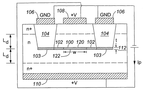
Figure 1 shows the basic structure of a photodetector embodying the invention,
without explicitly showing the electrical contacts. The basic structure of the
invention is a
finite width plasmon polariton waveguide 100 embedded in a semiconductor 112,
forming
a Schottky barrier photodetector. Two Schottky barriers are used in the
detection of the
signal, one on the top 120 and on the bottom 122 of the waveguide. The optical
signal for
detection, from a waveguide 140 (see Figures 3B and 5), will be endfire
coupled into the
waveguide 100 , i.e., directed into the page in Figure 1, and is shown in
Figure 4 as hv.
Where the photodetector is part of an integrated optics circuit, for example,
the waveguide
140 may be a part of that circuit, and could comprise another plasmon-
polariton waveguide
structure. Where the photodetector is a discrete component, however, the
waveguide 140
might be a "pigtail" of optical fiber packaged with the photodetector. It is
envisaged that the
waveguide 140 could be omitted and the optical radiation for detection coupled
from free
space in an endfire manner.
Figure 1 indicates how to reverse bias the Schottky barrier in both doping
cases.
When an n-type dopant is used, reverse biasing is achieved by establishing a
positive potential
diiTerence across the Schottky barrier, between the semiconductor 112 and the
waveguide
100, as shown in Figure 1A. When a p-type dopant is used, reverse bias is
achieved by
SUBSTITUTE SHEET (RULE 26)
CA 02514256 2005-07-25
WO 2004/079829 PCT/CA2004/000313
7
applying the opposite potential difference across the Schottky barrier,
between the metal
waveguide 100 and the semiconductor 112, as shown in Figure 1B.
Figures 2, 3 and 4 show the photodetector with a suggested electrode
configuration,
which is by no means the only configuration possible within the scope of the
present
invention. The electrode configuration comprises two ohmic contacts to the
semiconductor:
one contact 110 on the bottom and the other contact 108 on the top. The bottom
ohmic
contact 110 runs the length and width of the device, whereas the top ohmic
contact 108 runs
the length of the device but is narrower in. width than the device allowing
room for the
contacts to the waveguide 100.
The electrode configuration also comprises electrical contacts 102, 103, 104,
106
connecting to the waveguide 100 on either side. Electrical access to the
waveguide is enabled
through the contacts 106 on the top of the device, connected to contact
portions 103 by vies
104, in the form of trenches running almost the length of the semiconductor
body 112 but
stopping short at each end. The contact portions 103 are connected to the
waveguide 100 by
contact fingers 102, as illustrated in Figures 2, 3B and 4. The electrical
contacts to the
waveguide comprise contacts/electrodes on the top of the device 106 which
connect to
contacts at the waveguide level 103 through vies 104. The contacts at the
waveguide level
103 make contact to the waveguide 100 through optically non-invasive contact
fingers 102.
The optically non-invasive contact fingers have width, wf, of the same order
as the waveguide
width, w, as shown in Figure 3B, so as not to disrupt the plasmon polariton
mode as it
propagates along the waveguide. The contact finger length, Lf, is selected
such that the
contact portions 103 and vies 104 are positioned away from the plasmon
polariton mode
propagating along the waveguide 100. The thickness of the contact fingers 102
and the
contact portions 103 can be less than or equal to the thickness of the
waveguide 100.
The vies 104 which connect contact portions 103 to contacts 10G, could be, for
example, oppositely-doped semiconductor material as shown in Figures 2A, 2B,
and 4.
Alternatively, as shown in Figures 7A and 7B, which illustrate a modified
photodetector that
otherwise is identical to that shown in Figures 2A and 2B, the connectors may
be formed by
trenches 125 that have a lining 12G of insulation on side and end surfaces and
are filled with
metal to form a metal connector 127.
SUBSTITUTE SHEET (RULE 26)
CA 02514256 2005-07-25
WO 2004/079829 PCT/CA2004/000313
8
Figures 3A, 3B and 3C show the three different metalisation layers of the
device. The
top layer, shown in Figure 3A, comprises the contacts to the waveguide 106 and
the olnnic
contact to the semiconductor 108 that runs the length of the device. The
waveguide layer,
shown in Figure 3B, comprises the waveguide 100 and the contacts to the
waveguide 102
and 103. The contacts to the waveguide comprise contact portions 103 that run
alongside the
waveguide and contact fingers 102 that make contact to the waveguide. The
bottom layer,
shown in Figure 3C, comprises an ohmic contact 110 to the semiconductor that
runs the
length and the width of the device.
Figure 4 shows the relative position of the waveguide to the contacts 102,
103, 106,
108, 110 and vias 104. The ohmic contacts to the top 108 and bottom 110 of the
semiconductor are. used to bias both Schottky barrier contacts 120 and 122.
Taking
advantage.of the double Schottky barrier interfaces in this manner doubles the
surface area
of the Schottky barrier contact and increases the responsivity of the
photodetector. Of
course, only one barrier could be used, if desired or necessary.
It is possible to further increase the responsivity of the device by
introducing a
reflector.at the output of the waveguide. For example, as shown in Figure 5, a
Bragg grating
may be used as the reflector 130. The Bragg grating may be constructed using
the same
plasmon-polariton waveguide structure as the waveguide 100. The use of Bragg
gratings in
finite width plasmon polariton waveguides is disclosed by Jette et al in US
Patent Application
number 09/915,363 and International patent application PCT/CA01/01077 (~lO
0210815).
The reflector 130 would reflect otherwise lost radiation back into the device,
thereby
increasing the absorption and, hence, the responsivity without increasing the
area of the
Schottky barrier contacts. Since the dark current increases with the area of
the Schottky
barrier contact, keeping the area of the Schottky barrier constant keeps the
dark current
constant. Alternatively, in lieu of grating 130, a high reflection coating
could be used to coat
the back facet 128 of the detector.
As illustrated in Figures 1A and 1B, the type of doping used for the
semiconductor
can be either p-type or n-type. Metal-p-type semiconductor contacts typically
have lower
Schottky barrier heights which serve to increase the device responsivity but
also increase the
dark current, and hence, the minimum detectable power. Schottky barrier
contacts that
SUBSTITUTE SHEET (RULE 26)
CA 02514256 2005-07-25
WO 2004/079829 PCT/CA2004/000313
9
involve n-type semiconductors typically have higher Schottky barrier heights,
and, therefore,
have the opposite effect on responsivity, dark current, and minimum detectable
power.
The doping profile is designed to improve device performance based on
techniques
known in the art. Typically, higher doping levels in the semiconductor
material adjacent the
ohmic contacts reduce resistance at the ohmic contacts. Thus, Figures 1A and
2A, for n-type
material, and Figures 1B and 2B for p-type material, show the lower doping
levels extending
by a distance Ld each side of the strip 100.
A thin highly doped layer at the Schottky barrier interface has been used to
improve
detection and extend the wavelength range.by reducing the Schottky barrier
height. This
technique is described in U. S. Pat. No. 4,554,939 to Kosonocky et al, in U.
S. Pat. No.
4,908,686 to Maserjian, and in U. S. Pat. No. 5,648,297 to Lin et al.
Also, it is envisaged that oppositely-doped regions may be provided along the
length
of the strip 100 at opposite edges of the strip, i.e., the edges connected to
the contact fingers
102 (Figure 4), to control the dark current (leakage) at those edges of the
metal strip, again
using known techniques.
The positions of the contacts and vias, the doping width L~,, the width of the
contact
forgers wf, the number of contact fingers, and the period of the contact
fingers determine the
high speed characteristics ofthe photodetector. The contacts and vias need to
be laid out and
designed carefully to enable high speed operation by minimizing the parasitic
resistance,
capacitance and inductance of the photodetector. The number of contact fingers
required
should be minimised in order to be minimally optically invasive. The
dimensions of the
waveguide, the width, w, the thickness, t, and length, Lg, need to be designed
carefully to
achieve high responsivity and low dark current, and hence, low minimum
detectable power.
THEORY
To facilitate a proper understanding of how the photodetector operates and
before
the design of specific embodiments is described, the underlying theory, will
be discussed.
Light traveling along the waveguide 100 is attenuated by the waveguide 100
which
forms Schottky barriers 120 and 122 with the semiconductor. Most of the
attenuation is due
to photons being absorbed by carriers in the metal waveguide 100. In the
absorption process,
the photon energy is transferred to the carriers. This is called photo-
excitation. These photo-
SUBSTITUTE SHEET (RULE 26)
CA 02514256 2005-07-25
WO 2004/079829 ~ ~ ~PCT/CA2004/000313~ ~~'~ ~,.~,
excited carriers thus gain enough energy to be emitted across the Schottky
barrier, as holes
in the p-doped case, shown in Figure GA, and electrons in the n-doped case,
shown in Figure
6B, and produce a current in the semiconductor. This current h flows between
the ohmic
contacts 108/110 applied to (e.g. formed upon) the semiconductor material 112
and the
5 contacts 106 by way of the path defined by contacts 102, 103, vias 104 and
the waveguide
100. It should be appreciated that, if the vias 104 are wells of oppositely-
doped
semiconductor material, the contacts 106 also will be ohmic contacts.
The detection mechanism in embodiments of the present invention is the same as
in
prior art Schottky diodes; however, the internal quantum efficiency of
Schottky barrier
10 emission is increased in the thin film case due to an increase in the
probability of emission of
the photo-excited carriers. The internal quantum efficiency is usually defined
in the following
manner (H. Elabd and W. F. Kosonocky, "Theory and Measurements of
Photoresponse for
Thin Film PdZSi and PtSi Infrared Schottky-Barrier Detectors With Optical
Cavity," RCA
Review 43, pp. 569-589, 1982):
_ _N (1)
~' , N
T
where NT is the total number of possible excited states from which a photo-
excited carrier can
be emitted over the barrier ~B. This is consistent with the analysis by Cohen
et al in
"Investigation of Semiconductor Schottky Barriers for Optical Detection and
Cathodic
Emission," Air Force Cambridge Research Labs. Report No. 68-0651, 1968, and is
defined
as
r,~dN
NT ' ~ a'E dE (2)
where h v is the energy of the radiation, ~~ is the density of states
function, which is
assumed to be constant over the range of integration, and N is the number of
states from
which carrier emission across the barrier ~B may occur and is defined as
N = Jf d P(E~E ~ (3)
mB
SUBSTITUTE SHEET (RULE 26)
CA 02514256 2005-07-25
WO 2004/079829 PCT/CA2004/000313
11
where P(E) is the probability of emission of the photo-excited carriers.
If the density of states function is assumed to be constant over the range of
integration, combining equations (1), (2) and (3) yields the internal quantum
efficiency:
1 h~
~; = h ~ f P~E)dE (4)
mB
In the thick film case, the probability' of emission of photo-excited carriers
is defined
as (H. Elabd and W. F. Kosonocky, "Theory and Measurements of Photoresponse
for Thin
Film Pd2Si and PtSi Infrared Schottky-Barrier Detectors With Optical Cavity,"
RCA Review
43, pp. 569-589, 1982)
Pthick (E) = r~ 1 _ EB
where E is the photo-excited carrier energy in eV, E> Vie.
From equation (5), the internal quantum efficiency in the thick film case
becomes
z
1 1- ~B ~ (6)
~i,thick - 2 hV~
In the thin film case, with Schottky barrier interfaces on both sides, the
probability of
emission of photo-excited carriers is doubled due to the doubling of the
interfaces and is
further increased due to multiple carrier reflections within the film:
P(E) = Po + (1- Po )[P~ + (1- P )[P2 + ~1- PZ )~P3 +...+(1- Pn-I )~P" ~...~],
(7)
In the above probability equation, Po is the probability of emission at the
initial energy level
before any reflections have occurred, i. e. double the emission probability
ofthe thick film case
given in equation (5). Pk is the probability of emission at energy level Ek:
Pk=P(E,). Ek is the
energy of the photo-excited carriers after k reflections, Ek = Eoe kL , where
Eo is the initial
SUBSTITUTE SHEET (RULE 26)
CA 02514256 2005-07-25
WO 2004/079829 PCT/CA2004/000313
12
energy h v. L is the attenuation length of photo-excited carriers, t is the
metal thickness, and
n is the number of reflections for-radiation with energy h v, n = L In
t a
It can be seen that the internal quantum efficiency will increase with carrier
reflections
within the film. The number of carrier reflections depends on the ratio of the
attenuation
length of photo-excited carriers to the film thickness: Llt.. The attenuation
length of photo-
excited carriers is a property of the metal (including its structure) used in
the Schottky
barrier. The greater the Llt ratio the more the internal quantum efficiency
increases.
The external quantum e~ciency is defined in terms ofthe internal quantum
efficiency:
~7= Arlr
where A is the absorption, ~ = S°bs , where Sabs is the absorbed power
and S;"~ is the incident
st.»
power.
The amount of power absorbed depends on the coupling efficiency and the
absorption
of the device:
A = Y~ Aawr
where y~ is the coupling coefficient.
The absorption of the device can be calculated from waveguide attenuation
data. If
e~is the attenuation constant of the waveguide, the absorption of the device
is the follov~ing:
Aawr~e = 1- a 10
( )
where LR is the length of the waveguide.
The total absorption is therefore
A = Y~(1- e'~~'g ) (11)
Defined in terms of the external quantum efficiency, the responsivity is the
following:
R = ~ v (12)
Defined in terms of the internal quantum efficiency, the responsivity is the
following:
SUBSTITUTE SHEET (RULE 26)
CA 02514256 2005-07-25
WO 2004/079829 PCT/CA2004/000313
13
R Ahv (13)
where h v is in eV.
It should be noted that the responsivity depends upon the length of the
Schottky
barrier, the Schottky barrier height and the attenuation ofthe waveguide,
which itself depends
on the width and thickness of the waveguide metal. An explicit equation
showing these
relationships is given below for the thick film case:
2
_ a C 1 _ ~~1~
R = Y~ (1- a Lg ) 2h v ( 14)
The responsivity is also defined as a measure of the photocurrent produced for
a given
incident optical power:
R = IP (15)
Sr.»
To be detected, the photocurrent must be greater than the dark current which
is
defined according to the thermionic emission-diffusion theory (S. M. Sze,
Physics of
Semiconductan Devices, 2"'' ed. Wiley, New York, 1981, p262):
Idcrrk = ~'Lg~**~'ze ~' (16)
where wLg is the area of the Schottky contacts with m as the width of the
waveguide and Lg
as the length of the waveguide, T is the temperature in Kelvin, k is
Boltzmann's constant
(1.38054x10⁻²³ J/K), c~ is the electron charge (1.60218x10⁻¹⁹ C), and A** is
the effective
Richardson coefficient, which is 110AJcm2/K2 for electrons in n-type silicon
and 3 OAJcm2lK2
holes in p-type silicon (S. M. Sze, Physics of Senaiconductoy~ Devices, 2"d
ed., Wiley, New
York, 1981, p262).
The minimum photocurrent that can be detected corresponds to the minimum
incident
optical power that can be detected. From the responsivity equation (15), the
minimum
detectable power can be defined:
SUBSTITUTE SHEET (RULE 26)
CA 02514256 2005-07-25
WO 2004/079829 PCT/CA2004/000313
14
S -_ I min ( 17)
min R
where S",;n is the minimum detectable power and I,";" is the minimum
detectable photocurrent
which is defined as the lowest detectable current above the dark current. The
minimum
detectable photocurrent will be a function of the equipment used to measure
the output
current Ip of the photodetector. For comparative purposes, the minimum
detectable power
can be defined as being larger than the power at the dark current level:
S > Nark (18)
min R
Substituting the definition ofthe dark current from equation ( 16) into the
minimum detectable
power equation (18) yields
_ 9~a
wL A**TZe k''
Sm~, > 8 R ( 19)
It can be seen from the previous equations, (14) in particular, that the
responsivity
decreases as the Schottky barrier height increases but increases as absorption
increases, which
itself increases as the length and width of the waveguide, which is the
Schottky barrier,
increases. It can also be seen from (16) that the dark current decreases as
the Schottky barrier
height increases and increases as the Schottky barrier area increases. The
minimum detectable
power increases as dark current increases and decreases as responsivity
increases. Devices
with high responsivity and low dark current, or equivalently low minimum
detectable power,
are typically desired, however, responsivity and dark current both decrease as
the Schottky
barrier height increases and both increase as the length of the Schottky
barrier increases.
Because of these conflicting design requirements, it is not clear , which
photodetector
architectures will give the best performance characteristics without actually
comparing the
above equations to find the desired characteristics. For this reason; it was
important to
develop the theory for predicting the internal quantum ei~iciency of the
present invention.
Specific Examples of Preferred Embodiments
SUBSTITUTE SHEET (RULE 26)
CA 02514256 2005-07-25
WO 2004/079829 PCT/CA2004/000313
From the theory developed above, it is clear that both the Schottky barrier
height and
the Schottky barrier/waveguide dimensions affect the photodetector
performance. The length
and cross sectional area of the waveguide ai~ect the absorption; the longer,
wider and thicker
the waveguide the greater the absorption of light in the metal layer. The
surface area of the
5 Schottky barrier contact affects the dark current of the detector; the
larger the metal-
semiconductor contact area the greater the dark current. The greater the dark
current the
higher the minimum detectable power. Just as the waveguide dimensions have
conflicting
effects on the photodetector performance so does the Schottky barrier height.
The lower the
Schottky barrier, the higher the dark current and minimum detectable power but
the higher
10 the responsivity, as well. The absorption of the metal waveguide depends
not only on the
dimensions of the waveguide but also on the material selection. Depending on
the optical
parameters of the materials used, the attenuation will vary, and, hence, the
absorption will
vary. The absorption goes up as the attenuation goes up. Because of these
conflicting design
requirements on the dimensions and Schottky barrier height, it is not a simple
matter to
15 choose an appropriate material combination and associated dimensions. For
this reason,
design spaces for some material combinations have been generated and the best
designs
chosen from these are reported herein as preferred embodiments.
An example of a typical room temperature photodetector has been designed for
radiation at a wavelength of 1 SSOnm. The photodetector comprises a cobalt
disilicide-n-type
silicon Schottky barrier, which has a barrier height of 0.64eV according to S.
M. Sze, Physics
of Semicor~ducto~° Devices, 2"a ed., Wiley, New York, 1981, p292. Using
the attenuation
length for photo-excited (hot) electrons in cobalt disilicide of 9nm as
determined by Duboz
and Bodoz in "Hot-electron transport in epitaxial CoSi2 films," Physical
Review B, Vol. 44,
No. 15, 15 October 1991, the attenuation data for cobalt disilicide plasmon
polariton
waveguides in silicon calculated by the method described by Berini in U. S.
Pat. No.
6,442,321, and using the optical constants for cobalt disilicide determined by
Wu and
Arakawa in "Optical properties of epitaxial CoSi2/Si and CoSi2 particles in Si
from 0.062 to
2.76 eV," J. Appl. Phys. 71 ~(11), 1 June 1992, appropriate device dimensions
can be
determined. The thickness was chosen to be l5nm and the width was chosen to be
SSOnm,
at which, the attenuation of the waveguide is 258 dB/cm. When all of the
incident optical
power is coupled into the waveguide, a O.Smm long photodetector will have a
responsivity
SUBSTITUTE SHEET (RULE 26)
CA 02514256 2005-07-25
WO 2004/079829 PCT/CA2004/000313
16
of 0.0131 A/W and a minimum detectable power of about -40dBm. With a strong
reflector
at the output, the responsivity is increased to 0.0138A/W and the minimum
detectable power
remains the same.
If cobalt disilicide is used on p-type silicon, the responsivity will be
greatly improved.
For a cobalt disilicide layer with a thickness.of 20nm and length of 0.25mm,
photodetectors
have been designed for radiation at wavelengths of 13 l Onm and 1 S S Onm. In
the 13 l Onm case,
a waveguide with a width of 225nm will have an attenuation of 1347dB/cm, a
responsivity
of 0.1198A/W and a minimum detectable power of -24dBm. In the 1550nin case, a
waveguide with a width of SOOnm will have an attenuation of 792dB/cm, a
responsivity of
0.0962A/W and a minimum detectable power of -20dBm.
An example of a typical room temperature photodetector has been designed using
aluminum for detection of radiation at a wavelength of 131 Onm. The
photodetector comprises
an aluminum-p-type silicon Schottky barrier, which has a barrier height of
0.58eV according
to S. M. Sze, Physics of Semiconductoj° Devices, 2"d ed., Wiley, New
York, 1981, p. 291.
Assuming that the attenuation length for photo-excited holes is comparable to
that of photo-
excited electrons, the attenuation length for photo-excited electrons in
aluminum of 100nm
as determined by Quinn in "Range of Excited Electrons in Metals," Physical
Review Vol.
126, No. 4, May 15, 1962, 'can be used in conjunction with the attenuation
data for aluminum
plasmon polariton waveguides in silicon calculated by the method described by
Berini in U.
S. Pat. No. 6,442,321, and the optical constants for aluminum determined by E.
I~. Palik in
HandbookofOptical Constants ofSolids, AcademicPress, Inc., Orlando, 1985, to
determine
appropriate device dimensions. The thickness was chosen to be lOnm and the
width was
chosen to be l~.m at which the attenuation of the.waveguide is 95dB/cm. When
all of the
incident optical power is coupled into the waveguide, a 2mm long photodetector
will have
a responsivity of 0.0955 A/W and a minimum detectable power of about -35dBm.
The
responsivity value corresponds to an external quantum e~ciency of 0.0904 or
9%.
In order to achieve polarisation insensitive detection, the plasmon-polariton
waveguide disclosed in International patent application No. PCT/CA 02/00971,
i.e., with
width and thickness of the same order, could be used as the strip 100. With
this waveguide,
photo-excited carriers are emitted over the Schottky barriers formed at all
four sides of the
strip 100, i.e., at the four interfaces between the strip 100 and the
surrounding semiconductor
SUBSTITUTE SHEET (RULE 26)
CA 02514256 2005-07-25
WO 2004/079829 PCT/CA2004/000313
17
material. The theory presented in the previous section can be extended for
emission over four
barriers. Emission over four barriers results in increased responsivity,
albeit at the expense
ofincreased dark current.
It will be appreciated that, depending on the desired device performance
parameters,
many other material combinations and device dimensions can be used to build
embodiments
of this invention.
Generally, however, the length is chosen such that absorption is maximized.
The
absorption varies with the attenuation per unit length, so the length required
to maximize the
absorption will vary with the attenuation of the waveguide, which itself
varies with the width
and thickness of the metal waveguide strip.
In the above examples, the power of the plasmon polariton mode supported by
the
waveguide is substantially lower than its peak value a few micrometers from
the edge of the
waveguide. The contact finger length, Lf, should be chosen such that it is in
this range, i.e.
about S~,m.
It should be appreciated that, although the above-described embodiments use
both
strip/semiconductor interfaces as Schottky barriers, or all four in the case
of the "square"
waveguide strip, it would be possible to construct a photodetector using only
one
strip/semiconductor interface as a Schottky barrier. This would entail
providing the
semiconductor material on only one side of the strip with appropriate
reconfiguration of the
biasing contacts/electrode.
INDUSTRIAL APPLICABILITY
Embodiments of the present invention provide an alternative solution to the
integration problem, having the advantage that substantially total absorption
of the incident
light can be achieved when designed correctly. Photodetectors according to the
present
invention can operate over a much broader wavelength range than the surface
detectors and
surface plasmon detectors discussed hereinbefore and, as compared with the
endfire
photodetector disclosed by Yang et al in U. S. Pat. No. 4,857,973, can achieve
much higher,
if not total, absorption of the incident light and provide better responsivity
for a given dark
current.
SUBSTITUTE SHEET (RULE 26)
CA 02514256 2005-07-25
WO 2004/079829 PCT/CA2004/000313
18
In embodiments ofthe present invention, the finite width metallic waveguide
functions
as the Schottky barrier photodetector, as well as the waveguide, allowing
total absorption of
the incident light without narrowing the bandwidth. The fact that the
photodetector is an
endfire excited planar device facilitates its integration with other optical
and electrical devices.
The use of silicon as the semiconductor improves the integration possibilities
by allowing
integration with CMOS, BiCMOS and Bipolar processes and electronics.
SUBSTITUTE SHEET (RULE 26)