Note: Descriptions are shown in the official language in which they were submitted.
CA 02514813 2009-09-03
1
MEMO AND APPARATUS FOR MEASURING POLARIZATION MODE
DISPERSI:ON.
DESCRIPTION
TECHNICAL FIELD:
This invention relates to a method and apparatus for measuring polarization
mode
dispersion (PMD) in optical devices, especially in waveguides such as are used
in optical
communications systems.
BACKGROUND ART:
It is well known that PMD may be measured by injecting wideband linearly
polarized
light into the wavegu:ide, passing the light leaving the waveguide through a
linear polarizer
and then sending it to a scanning interferometer, recombining the light from
the two arms
of the interferometer to produce interferograms, converting the recombined
light izxtensity,
I, into a corresponding electrical signal and processing the electrical signal
to extract the
PMD from a curve, T(t), of intensity I against the path delay difference i
between the two
arms of the interferometer (referred to hereinafter as delay -r),
As explained in United States patent number 5,712,704 (Martin et al.), the
curve I(z)
exhibits a high central peak, with smaller fluctuations that can be seen on
either sxde.
(Similar fluctuations at the centre are masked by the central peak.) The
central peak is
representative of the light spectrum at the output of the waveguide (before
the linear
polarizer) while the fluctuations represent the PMD, According to Martin et
al., this peak
"hinders the processing of the detected signal, thereby constituting an
obstacle to the
accurate measureznent of the PMD",
Martin et al, discussed a previously-disclosed technique which retnoved the
central
peak by passing the light by way of a first polarizer at 45 to an
interferometer having a
polarizer at 0 in one arm and a polarizer at 90 in its other arm, and
passing the recombined
light through an analyzer (analysis polarizer) at 0 . Having identified
complex construction
and the use of the analyzer as unsatisfactory, Martin et al. sought to provide
a simpler way
ofrenn,oving the central peak. In particular, Martin et al. provided at least
one birefrin.gent
element having two independent modes of polarization in at least one oI'the
arms of the
CA 02514813 2009-09-03
2
iztterferozzteter, the algebraic sum of the elementary phase shifts in the two
arms being equal
to a relative phase shift and the algebraic difference between the two
relative phase shifts
having a value of n. According to Martin et al., this allows the curve of
intensity I against
delay t to be obtained without the "parasitic" central peak.
Neither of these approaches is entirely satisfactory, however, because they
are
predicated upon removal of the "parasitic" central peak on the grounds that it
detracts fram
the measurement of PMD, so that simple removal of the central peak should
significantly
improve measurement accuracy. Thxs is only true in part. In fact, removing the
central peak
means that useful information is discarded, as a result of which very small
P1V1llls, tending
towards zero, cannot be measured accurately. In practice, improvement of
measurement
accuracy is marginal.
DISCI..OSURE OF INVENTYON:
The present invention seeks to at least mitigate the deficiencies ofthese
lsio'tx+n PMD
measurement techniques, or at least provide an alternative.
According to one aspect of the present invention, apparatus for measuring
polarization mode dispersion (PMD) of a device, for example; a waveguide,
comp;rises:
(1) broadband light source means for applying polarized broadband light to one
end of
the waveguide,
(ii) an interferometer having an input port and an output port, means for
dividing said
light from the waveguide into first and second components, first and second
paths for
conveying the first and second coxnponents, respectively, to said output port
for
recombination, and means for varying the length of one of the first and second
paths
relative to the other to cause interference betweerx the components upon
recombination,
(iii) a polarization separator for receiving the recombined light from the
output port and
separating said recombined light along two orthogonal polarization states to
obtain
corresponding first and second interferograms,
(iv) first and second detection means for converting the first and second
interferograms,
respectively, into corresponding first and second electrical interferogram,
signals
~x(z),1',,,('r)), and
CA 02514813 2009-09-03
3
(v) processor means for processing the first and second electrical
interferogram signals
to produce a cxoss-correlation envelope (EC(2)) and an auto-correlation
envelope
(EA(T)), and determining from the cross-correlation envelope and auto-
correlation
envelope the polarization mode dispersion (PMD) of the waveguide.
According to a second aspect of the invention, a method of measuring
polarization
mode dispersion of device, for example, a waveguide, comprises the steps of :
(i) passing polarized broadband light through the waveguide;
(ii) using an interferometer, dividing and recombining the light leaving the
waveguide to
produce interferograms;
(iii) separating the recombined light into first and second interferograms;
(iv) converting the first and second interferograms, respectively, into
corresponding first
and second electrical interferogram signals (Px(i),Py(z)), and
(v) processing the first and second electrical interferogram signals to
produce a cross-
X5 correlation envelope (Ec(ti)) and an auto-correlation envelope (EA(~)),
respectively,
and determining from the cross-correlation envelope and the auto-correlation
envelope the polarization mode dispersion (PMD) of the waveguide.
In embodiments of either aspect of the invention, the cross-correlation
envelope
(Ec(ti)) may be computed as the modulus of the difference between the first
and second
electrical interferogram signals and the auto-correlation envelope (EA(C)) as
the modulus of
the sum of the first and second electrical interferogram signals according to
the expressions:
E,(T) =IPx(T) -Py('i)I 2171dEA(T) =IPX(Z) + PY(t)I
Preferably, the polarization mode dispersion (PMD) is computed from the cross-
correlation envelope (Ec(ti)) and the auto-correlation envelope (EA(ti))
according to the
expression
PMD 2 (62 o)
f TzEC ( Z) dt 2 'L2EA
2 ( t) dt
where ¾ = and ao =
fEG2 (T)dt fEA2 (t)dz
CA 02514813 2009-09-03
4
and T is the delay between the first and second paths of the interferometer.
BItrEF DESCRIPTION OF THE DRAWINGS:
An embodiment of the invention will now be described by way of example only
with
reference to the accompanying drawings, in which:
Figure 1(a) labelled PRIOR ART illustrates conventional apparatus for
measuring
polarization mode dispersion (PMD) of a waveguide under test;
Figure 1(b) illustrates the power spectrum, as a function of optical frequency
v, of
light leaving an analyzer in the apparatus;
Figure 1(c) illustrates the fimnge envelope, as a function of the delay T, at
the output
of an interferometer in the apparatus;
Figure 1(d) illustrates, with the help of power spectxum the physical origin
of auto-
correlation and cross-correlation parts of the fringe envelope; and
Figure 2 illustrates an embodiment of the present invention.
DETAILED DESCRIPTION OF PREFERRED EMBODIMENTS:
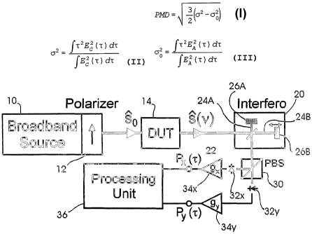
The known apparatus illustrated in Figure 1 comprises a broadband polarized
lxglat
source means comprising a broadband Iight source 10, for example a light
emitting diode,
erbium doped fiber source, and so on, and a polarizer 12 (conveniently a
linear polarizer) for
polarizing the light from source 10 and applying the polarized light, with
state ofpolarization
"sa, to an input of a device-under-test (DUT) 14, for example an optical fibre
or other kind of
waveguide. Light leaving the DT..JT 14 and having an optical frequency
dependent state of
polarization "s(u) and power Po(v) is applied via an analyzer 16, conveniently
another linear
polarizer, to an input port 18 of an interferometer 20, shown as a Michelson
interferometer.
The interferometer 20 comprises a splitter or separator 22, for example a
serni-
reflective plate inclined at 45 or a 50-50 fibre coupler, for splitting the
light received from
the analyzer 16 into two component interference beams 24A and 24B,
respectively, and for
recombining the interference beams, following their reflection by mirrors 26A
and 26B,
respectively, to form a recombined light beam which leaves the interferometer
20 via au
output port 28.
CA 02514813 2009-09-03
Mirror 26A is fixed while mirror 26B is movable to vary the length of the path
traversed by interference beam 24B relative to that traversed by interference
beam 24A. In
operation, the scanning mirror 26B is moved to and fro to vary the path length
and hence the
path delay difference r between the two anns so that the interference beams
24A and 24B
5 interfere when recombined at the output of the interferometer 20. Figure
1(c) shows the
resulting interferogram at the output port of the interferometer 20 (more
precisely the
interference fringe envelope, oz- ftinge visibility as a function of delay -
c).
As shown in Figure 1(b), when there is an analyzer 16 at the output of DUT 14,
the
spectrum of the light entering the interferometer 20 may have an overall bell
shape, but with
luge fluctuatxons, In effect, the interference fringe envelope produced by
interferometer 20,
shown in Figuze 1(c), is the rnodulus of the Fourier transform of the
spectrum. Figure 1(d)
xllustrates the derivation of the interferogram from the following expression
for the spectrum:
P(v) = ZP(v)11+s(v)-ea~ (1)
where GQ is the maximum transmission axis of the analyzer 16, I',(v) is the
optical power
as a function of the optical frequency before the analyzer 16, and 1'(v) is
the optical power as
a function of optical frequency after the analyzer 16.
As can be seen from Figures 1(c) and 1(d), and the term in the square brackets
in
equation (1), the spectrum of the light leavin.g the analyzer 16 can be
expressed as the sum
of the two parts, one part being independent of the state of polarization
(v); the so-called
central peak originates from this part. The central peak is the auto-
correlation, i.e. the
modulus of the Fourier transform of the spectnun Po(v) at the input of the
analyzer 16 (see
Figure 1(d)), it is independent of the fluctuations of the state of
polarization s( v) and hence
of the PMD. It should be noted that the maximum of the auto-correlation peak
at the centre
(delay = 0) has been set to 1; the graph is scaled to show the cross-
correlation part more
clearly.
The second part of the term in the square brackets in equation (1) is
dependent upon
state of polarization and results in the cross-correlation part of the
interferogram in Figure
CA 02514813 2009-09-03
6
1(d); it has some given value at the center, but no large central peak. It
should be noted that
Figure 1(d) is provided simply to facilitate a basic understanding. This
apparatus measures
interferograms directly; no spectrum is measured.
In such a conventional interferometric PMD measuring apparatus, the overall
envelope in Figures 1(c) and 1(d) is not the sum of the two envelopes, i.e.,
auto-correlation
and cross-correlation; they interfere in the centre portion (modulus of sum,
not sum of
modulus). Where the PMD is relatively large, e.g.,10 ps, the width of the
cross-correlation
envelope is much largex than the width of the auto-coyrrelation peak, so the
presence of the
auto-correlation peak is not of great cotacer,o, It should be noted that the
maximum of the
auto-correlation peak at the centre (delay = 0) has been set to 1: the scale
of the graph is
increased in order to show the cross-correlation part more clearly.
The approach taught by US5,712,704 is to remove this auto-correlation peak by
omitting the analyxer and inserting a waveplate in one arm of the
interferometer 20. This is
not entirely satisfactory, however, because it discards information that is
particularly useful
when measuring very low values of PMD. This so-called parasitic central peak
is not just a
parasite. Knowledge of it, obtained by extracting both the cross-correlation
and the auto-
correlation, separately, without one interfering with the other at center, can
be used to great
advantage.
Thus, embodiments of the present invention do not discard the auto-correlation
peak
but rather use it to improve the accuracy of the PMD measurement, especially
where PMU
is very small. Such an embodiment will now be described, as an example, with
reference to
Figure 2 in which components corresponding to those shown in Figure 1(a) have
the same
reference numerals. The operation of the apparatus shown in Figure 2 is
similar in many
respects to that of the apparatus shown in US5,712,704 and so, for
convenience, will not be
described in detail here. For further information, the reader is directed for
reference to
US 5,712,704.
The apparatus shown in Figure 2 differs from that shown in Figure 1(a) in that
the
analyzer 16 is omitted and a polarization beam splitter (PBS) 30 is disposed
with its input
port coupled to the output port 28 of the interferometer 20 and its output
ports coupled to first
and second photodetectors 32x and 32Y, respectively. The electrical outputs of
the
CA 02514813 2009-09-03
7
photodetectors 32x and 32Y, (optionally) amplified by amplifiers 34x and 34,,
are moz:utored
by a processor 36.
The PBS 30 splits the recombined light beam into two interferogram components
Px(t) and PY(ti) having mutually orthogonal states of polarization, and
supplies the two
interferogram components to the photodetectors 32x and 32Y, respectively, for
conversion into
corresponding electrical signals which are amplified and supplied to processor
36.
The processor 36 processes the electrical signals to extract the
interferograms for both
states of polarization and uses thena to compute the PMD of the DUT 14. More
particularly,
the processor 36 obtains the auto-correlation envelope EA(i) and cross-
correlation envelope
Ec(t) by computing the sum and difference of the electrical signals from the
two
photodetectors 32x and 32Y. Thus, where PX(T) and PY(ti) are the two
interferograms as
functions of the delay diffez'ence r between the two arms of the
interferometer 20, Auto-
correlation E,,(ti) and Cross-correlation Ec(T) are derived as follows:
EA(-E) = iP (ti) +PY(2) I and Ec(Z) =JPx(t) -PY(Y) 1 (2)
The main difference in the subsequent processing, as compared with that
described
in US5,712,704, is that the PMD is computed using the expressiou
Q2 - a') (3) i,
PMD = 2 (
o
where 60 2 is the rrns width of the squared auto-correlation envelope, just as
a is the rms width
of the squared cross-correlation envelope. The formula used to obtain a and a4
is the same
in both cases as follows;
fYzEI
c (z)dt fT2E.'2 (T)dT
4
(~) dT and cro rEA ( i) dt ()
a fE2 2
As can be seen from equation (3), a known offset ao is subtracted from a2 to
obtain
the PMD value; ao is indeed independent of the PMD value since, according to
equation (4),
it is deduced from the separate auto-correlation envelope. Thus, owing to the
fact that both
the auto-correlation envelope and the cross-correlation envelope are extracted
separately,
CA 02514813 2009-09-03
8
without one interfering with the other, the offset ao can be computed
according to equation
(4) and subtracted from az according to equation (3).
The following practical advantages follow from knowing and subtracting this
offset
c~a, when computing PMD:
1. Independence from the spectrum shape: the technique becomes insensitive to
the
width and shape of the spectrum Po(n), notably insensitive to ripples on the
spectrum (e.g.
multi-path interference (MPI) effects), filtering by the DUT, etc.), which
phenomena
currently are true practical limitations of commercially available
Interferometric PMD
analyzers. Whatever the shape of the spectrum, it actually translates as an
offset ao on the
observed c~,
2. Measraxemeiat of PMD as snnall as PMD = 0: It should be appreciated that,
when the
PMD value is small, i.e. not so much larger than ao or in the same order of
magnitude,
knowing the offset is more than a marginal advantage. In fact, embodiments of
the present
invention are truly capable of retuming the result PMD = 0, when PMD = 0,
which is not the
case with currently available analyzers which, when PMD 0, return a PMD vaXue
zao 3,
i.e. the offset value. Of course, when PMD is large, this may not be a concem.
3. Measurement tkrough EDFAs (Erbium-Doped Fibre Aztxplifiers) is facilitated:
as a
corollary, the above-described properties of embodiments of the present
invention make it
possible in practice to use the interferometric PMD analyzer for measuring
fibre links that
comprise EDFAs, which is very advantageous.
When going through an EDFA, the spectrum at the output of the link is nnuch
narrower than the spectrum of the input broadband source, and does not have a
smooth shape.
Consequently, the auto-correlation width (ao) is much larger than it is when
measuring a
typical "passive" fibre (noting that, as shown in Figure 1(d), the auto-
correlation
interferogram is the Fourier transform of the specttm of the light at the
input of the
interferometer (with no analyzer, as in Figure 2)). Moreover, and obviously,
the spectrum
after going through EDFA's cannot be considered to be known in advance with
precision in
all cases. In essence, measuring the auto-correlation in addition to the eross-
cozrelation is
CA 02514813 2009-09-03
9
measuring the only characteristic of the spectXUm that has to be known
according to equation
(3), i.e. the rms width of the corresponding auto-correlation 6o, (squared).
With EDFAs, ao
may be in the picosecond range instead of- 30 fs when there is only the fibre.
That cannot
be ignored as "negligible".
It should be noted that there is also unpolarized noise at the output when
there is an
ETaFApresent since, like electronic amplifiers, optical amplifiers have a f
nite "noise figure".
The cross-correlation interferogram does not contain a contribution of the ASE
noise to a.
Nevertheless, this constitutes a limitation because interferograms (fringes)
are in fact
superimposed on a constant offset (total power), i.e., constant as a function
of delay T. Thus,
if ASE is too large, it means that the signa]/noise ratio can be significantly
degraded in
practice.
It should be appreciated that the processor 36 may have means for storing the
two
observed interferograms, Px(T) and PY(r), in order to be able to compute
afterwards the sum
and difference according to equations (2). (possibly using a sep2irate
computer).
Alternatively, the processor 36 may be arranged to compute the sum and
difference in real
time (electronically, analogically, or numerically).
Various other modifications are envisaged within the scope of the present
invention.
For example, the PBS 30 could be replaced by an ordinarybeamsplitter (i.e. not
polarization-
selective), and two polarizers, each placed in front of one of the two
photodetectors, one
polarizer with its axis orthogonal to the axis of the other. Alternatively,
again with a-n
ordinary beamsplitter instead of a PBS 30, one polarizer could be placed in
front of one
photodetector, and no polarizerplaced in front of the other, to obtain
interferograms P,,(i) and
Po(z) respectively; in this latter case, the calculation to deduce auto-
correlation and cross-
coxxelation envelopes from the two raw interferograms differs from equation
(2), but stilZ
employs simple sums and differences, as follows:
Ec(z) = (2Px(i) -Po(t) I and Ea(T) = IPo(i) ~ (5)
It is envisaged that the invention couId be implemented using detection along
any two
"distinct" polaxi.zation axes (distinct meaWng "not strictly identical),
provided that they are
precisely known (i.e. the angle between the two axes is precisely known). They
need not be
orthogonal (at 1 $0 on the Poincard spb,ere),
CA 02514813 2009-09-03
.'~
The invention is not limited to the measurement of PMD in waveguides, e.g.
fibers
+ 'r!
(even multimode fibers), but is also valid for "open space" or "bulk" optical
devices, or
optical components with integrated waveguides. Basically, the DUT 14 may be
any device
whose light output can be collected into a substantially collimated beam.
Other options
5 include:
the `bulk" device can have fibez pigtails at input and output;
the interferometer can have a fiber input (with a lens to form a collimated
beam);
a collimated beam can be lawnched into the interferometer with no fiber input.
While the above-described embodiment has a schematic Michelson interferometer,
10 more specifically the simpler Michelson interferometer, with one arm of
fixed delay, it would
be feasible to use a Michelson interferometer with the delays of the two arms
varying, but
with only one, two-sided moving mirror: the delay in one arm decreases wben it
increases in
the other arm, and vice-versa: this doubles the delay range that is scanned
with a given
physical travel of the moving mirror.
Alternatively a Mach-Zehnder type of interferometer could be used, in which
there
is no mirror, the two paths simply being recombined on a second output
beamsplitter.
Whether a Michelson type or Mach-Zehnder type, the interferometer may be a
fiber
interferometer: the "fzee-space" beamsplitter(s) being replaced by a fiber
coupler.
Generally, therefore, embodiments of the invention may explore any two-path
interferometer with a variable path delay difference, that recombines the
light from the two
paths into one common path, i.e. into one fiber or into two substantially
superimposed light
beams (not necessarily collimated, providing the two beams from the two paths
have
substantially the same direction of propagation and radius of curvature of the
wavefronts)
+ Pr