Note: Descriptions are shown in the official language in which they were submitted.
CA 02515415 2005-08-08
WO 2004/073366 PCT/US2004/004185
CIRCUIT BOARD AND SOCKET ASSEMBLY
BACKGROUND OF THE INVENTION
Field of the Invention
The present invention relates generally to electrical connectors. More
particularly, the
present invention relates to. a method of and system for interconnecting a
printed circuit board
to the rear of an electrical socket or plug.
Description of the Prior Art
Present methods of and systems for terminating a printed circuit board to the
rear of
an electrical socket or plug connector include soldering the connector contact
tails to the
board. The purpose of the soldering .operation is to provide electrical and
mechanical
connection. In some instances, the heat generated by the soldering process can
adversely
effect the connector and printed circuit board. As a result, the electrical
performance of the
interconnect can be irreparably destroyed or, at the least, significantly
degraded.
Performance degradation, of course, must be avoided in electronics devices
that are used in
avionics and other sensitive systems, especially where rigid specifications
must be met.
Moreover, soldering can create a rigid connection between the components. When
a
member soldered to a printed circuit board is deformed due to tensile,
compressive or torque
forces acting on the member, those forces can be propagated or transferred
into the substrate
of the printed circuit board causing internal stress. The stress can then
damage the substrate
or the crystal lattice structure associated with the circuits on the printed
circuit board
resulting in damage to the device. .
The present method solves the problems associated with soldering and rigid
connections by providing an interconnect between a socket and a printed
circuit board
whereby the means for attaching the two components together is made without
soldering or
using other methods involving heat. Moreover, .the present invention solves
that problem
without introducing new problems, such as causing internal stresses in the
printed circuit
board that can also result in penormance degradation.
-1-
CA 02515415 2005-08-08
WO 2004/073366 PCT/US2004/004185
Solderless interconnects are not new. U.S. Patenl
example, discloses a cylindrical connector contact for an electrical socket
that can be mated
to a printed circuit board. The contact, like in the present invention,
provides the means for
attaching the socket to the printed circuit board. The contact is made of a
conducting
material so that there is electrical continuity between an electrical
conductor inserted in the
front end of the contact and the circuits on the printed circuit board. In
Sutfliffe, the contact
has a plurality of axially spaced "barbs" arranged in a purely circumferential
direction on the
distal or "tail" portion of the contact. Those barbs engage rings on the wall
of a circuit board
through hole thereby retaining the contact within the hole. The larger the
diameter of the
hole, the greater the number of rings and barbs that are needed to ensure
adequate mechanical
attachment. Sutcliffe teaches that at least two barbs and rings are required
to achieve a stable
electrical contact. To allow for dimensional tolerances to be relaxed, the
tail includes an
axial cut so that the tail portion becomes flexible, which could reduce
internal stresses on the
printed circuit board at the connection point.
There are several problems associated with the contact disclosed in Sutcliffe.
First, it
is difficult and expensive to manufacture barbs and rings with tolerances in
the order of a few
hundredths of an inch. Moreover, if the contact is inserted in the printed
circuit board
through hole too far, only one barb and ring may make contact, reducing the
electrical
continuity between the two components and also lowering the mechanical forces
retaining the
contact in the hole. Further, only a portion of barb actually makes contact
with a ring inside
the hole, which limits the amount of electricity that can be conducted between
the two parts.
U.S. Patent No. 4,374,607 to Bright et al. also discloses an interconnect that
does not
require soldering but, unlike Sutcliffe, uses axially spaced "undercuts" or
teeth on the distal or
tail portion of a pin contact to mate with corresponding axially spaced
grooves on a socket.
When inserted, the undercuts engage and retain the contact in the socket.
The ~ problem with the pin contact disclosed in Bright et al. is that
electrical
conductivity is made at the very distal end of the contact, which would not be
feasible if it
were used to conduct electricity to a printed circuit board. Pin contacts used
for printed
circuit boards generally require electrical contact at or near the same point
where mechanical
attachment occurs. That type of connection is preferred in many cases because
the tensile
and compressive forces transmitted through the contact to the printed circuit
board must be
minimized, as noted above, to reduce internal stresses on the board. Internal
stresses can
-2-
CA 02515415 2005-08-08
WO 2004/073366 PCT/US2004/004185
damage the crystal structure of, for example, the logic circui
failure.
U.S.,Patent No. 4,701,004 to Yohn discloses a solderless cylindrical retention
clip for
receiving an electrical contact pin of an electrical connector. The clip is
inserted inside a bore
hole. One end of the clip includes two ~ cantilevered springs or lances
projecting radially
inward toward the longitudinal axis of the clip. The ends of the springs
engage a shoulder or
groove formed on a pin. The shoulder extends perpendicular to the longitudinal
axis of the
pin (i.e., radially).
One obvious problem with the retention clip disclosed in Yohn is that it is
not
designed to conduct electricity. So while a contact inserted in the clip is
retained and
prevented from moving in a direction longitudinal to the contact axis, no
electrical signals are
conducted through the clip to another system.
U.S. Patent No. 4,050,772 to Bir~zholz et al. discloses a contact pin and
printed.circuit
board through hole receptacle for receiving the contact and conducting
electricity. The
through hole receptacle includes a rectangular lip around the opening of the
hole and an
annular electrical contact surrounding the opening of the hole. Together,
those components
engage the rear shoulder of a flange at the top of a contact pin as it is
inserted in the hole.
Another portion of the through hole inside the hole engages a radially-
extending shoulder of
a barb on the shank of the contact.
The problem with the contact pin disclosed in Birrzlaolz et al. 'is that the
rigid metal
barb of the contact forces the plastic hole apart during insertion of the
contact. That' can
cause internal stresses within the printed circuit board in the vicinity of
the through hole that
can damage the performance of the device. Also, the contact through hole
receptacle forms a
rigid connection with the contact, which is disadvantageous in some
applications as noted
previously.
The various approaches described in the above-cited patents for making
solderless
interconnects have not been found to be totally satisfactory solutions. This
is especially true
in the context of electrical interconnects used in highly demanding
applications like aircraft
connectors.
-3-
CA 02515415 2005-08-08
WO 2004/073366 PCT/US2004/004185
SUMMARY OF THE INVENT
In view of the foregoing, it should be apparent that there still exits a need
in the art for
a method and apparatus for electrically interconnecting an electrical socket
and a printed
circuit board in which there is good conductivity and retention between those
components
and wherein the means fox interconnecting does not degrade the electrical
performance of the
device. It is, therefore, a primary object of this invention to provide a
method and apparatus
fox interconnecting a printed circuit board to the rear of an electrical
socket that does not
require soldering or other methods involving heat.
More particularly, it is an object of this invention to provide a conducting
contact or
pin associated with an electrical socket that extends into and engages a
conducting through
hole on a printed circuit board without the need for soldering.
Still more particularly, it is an object of this invention to provide a
conducting contact
or pin associated with an electrical socket that extends into and engages a
conducting through
hole on a printed circuit board so that external forces acting on the socket
or plug are not
transferred through the contact point to the printed circuit board or vice
versa and thereby
cause damage to the device.
Another object of this invention to provide a contact receptacle in a printed
circuit
board through hole that has springs or flanges for engaging an undercut on a
contact when the
contact is inserted in the contact receptacle.
A further object of the present invention is to provide a contact insertable
in a contact
receptacle in a printed circuit board in which the point where those
components touch
provides longitudinal retention of the contact in the receptacle and also
provides electrical
continuity between the components.
Still another object of the present invention is to provide a contact and
contact
receptacle in a printed circuit board in which the contact minimizes the
transfer of internal
stresses between the electi~cal socket and the printed circuit board.
Briefly described, these and other objects of the invention are accomplished
in
accordance with its apparatus aspects by providing a contact associated with
an electrical
socket receptacle or plug assembly and a contact receptacle associated with a
through hole on
a printed circuit board assembly. Thus, the contact can be associated with
either a plug or a
socket. In either case, the contact has a proximate or front end with a cavity
for receiving an
-4-
CA 02515415 2005-08-08
WO 2004/073366 PCT/US2004/004185
electrical conductor of a plug, and a distal or rear end, al
circumferentially arranged undercut that engages the ends of one or more
electrically
conducting flanges that extend radially inward in the contact receptacle. The
receptacle
assembly can be any receptacle, including one adaptable for receiving a round,
14-conductor
plug, and includes a front and rear shell and an insert slidably engaged
inside the rear shell.
The printed circuit board assembly includes a printed circuit board with one
or more contact
receptacles, rear insert, retainer spring, and chip capacitor board.
With these and other objects, advantages and features of the invention that
may
become hereinafter apparent, the nature of the invention may be more clearly
understood by
reference to the following detailed description of the invention, the appended
claims and to
the several drawings attached herein.
-5-
CA 02515415 2005-08-08
WO 2004/073366 PCT/US2004/004185
BRIEF DESCRIPTION OF THE DR,
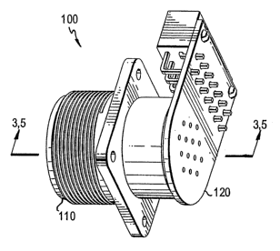
FIG.1 is a perspective view of the connector of the present invention;
FIG. 2 is an exploded perspective view of the connector of the present
invention
showing its individual assembly components;
FIG. 3 is a cross-sectional view of the connector of the present invention
taken at line
3-3 shown in FIG.1;
FIG. 4 is an enlarged, partial, cross-sectional view of the contact component
of the
present invention shown partially inserted in the contact receptacle component
of the
invention; and
FIG. 5 is another enlarged, partial, cross-sectional view of the present
invention
showing multiple contacts.
-6-
CA 02515415 2005-08-08
WO 2004/073366 PCT/US2004/004185
DETAILED DESCRIPTION OF THE I
Referring now in detail to the drawings, wherein like parts are designated by
like
reference numerals throughout,. there is illustrated in FIG. 1 a perspective
view of the
electrical connector 100 of the present invention having receptacle assembly
110 and printed
circuit board assembly 120 in mating contact. The connector 100 in FIG. 1
illustrates how a
socket and printed circuit board embodiment of the invention could be used in
a typical
application. It will be appreciated by one of ordinary skill in the art to
which the invention
pertains, however, that any connector involving the interconnection of a
socket receptacle,
pin receptacle or a plug and a panted circuit board is contemplated by the
present disclosure
and the invention can be used in many environments benign or severe as in
aircraft. For
example, the socket receptacle embodiment illustrated in FIG. 1 can be
adaptable to receive a
plug of any shape, not just round ones.
In the context of the present invention, the word "socket" can be interchanged
with
"adapter" or "receptacle." Those terms, and others commonly used in the art,
refer generally
to the female portion of an electrical interconnect. The word "plug" generally
refers to the
male portion of an electrical interconnect, although other terms are often
used, including the
general term "connector." However, "connector" also refers generally to a
physical
connection or mating of electrical components. It is important to note that a
receptacle or a
plug can contain pin or socket contacts. The embodiment of the connector 100
illustrated in
FIG. 1 has a socket contact in a receptacle connector.
In FIG. 2, there is illustrated an exploded perspective view of the electrical
connector
100 of FIG. 1 showing the individual assembly components of the receptacle
assembly 110
and printed circuit board assembly 120. The receptacle assembly 110 includes a
receptacle
210 and a contact 230. The printed circuit board assembly 120 includes a
printed circuit
board 251 and, in the embodiment shown, a printed circuit board plug
receptacle 259. In
FIG. 2, the assembly of components shown forms an electrical filter connector
having a total
capacitance of up to about 100,000 picofarads.
The components of the receptacle 210 include the following. First, the
receptacle 210
has an opening 211 at a front end that is substantially cylindrical. In the
embodiment shown
in' FIG. 2, the cylindrical opening 211 is designed to receive a plug size 20
in accordance
CA 02515415 2005-08-08
WO 2004/073366 PCT/US2004/004185
military specification standard MIL-C-5015. However, the
size and shape in accordance with other standards.
Next, the receptacle 210 includes a cylindrical, threaded front shell 212 that
forms the
opening 211. Obviously, the front shell 212 does not have to be threaded, as
any method of
attaching a plug to the shell 212 is contemplated, including, but not limited
to, the use of a
clamp ring (not shown). The front shell 212 is axially-aligned with a rear
shell 214. The
front shell 212 and rear shell 214 are axially separated by a flange 213
interposed between
those components. In FIG. 2, the flange is rectangular; however, a different
shaped flange
could also be used,. depending on the specific application in which the
connector 100 is used
(in some cases, no flange may be required). Preferably, the front shell 212,
flange 213 and
rear shell 214 are made of one piece nickel plated aluminum alloy.
Next, the receptacle 210 includes a socket insert 215, which in FIG. 2 is
shown as a
cylinder with at least one longitudinally-extending contact hole 216 (only the
rear opening of
the hole 216 is shown). The socket insert 215 is slidable inside the front and
rear shells 212,
214 and aligned axially in the shells 212, 214 by an insert retainer shoulder
217 located at the
distal or rear end of the socket insert 215. The retainer shoulder 217 has a
slightly larger
diameter than the socket insert 215 and includes an alignment groove 218 that
engages an
axially-extending flange (not shown) on the top inside surface of the rear
shell. 214. Thus
engaged, the alignment grove 218 prevents the socket insert 215 from rotating
in a
circumferential direction inside the shells 212, 214. As described in more
detail below, a heat
activated adhesive is applied to shoulder 217 and cured 'in an oven to
stabilize and fix the
socket insert 215 in place preventing rearward movement. A rear insert seal
254 (discussed
below) prevents the socket insert 215 from backing out of the rear shell 214
after assembly.
As noted above, socket insert 215 includes at least one contact hole 216
(described
below), for receiving a contact. The socket insert 215 will have one contact
hole 216 for each
electrical conductor associated with a mating plug (not shown). In FIG. 2,
only one contact
hole 216 is shown for clarity.
Next, the receptacle 210 includes a chip capacitor board 257. A retainer
spring 256 is
axially-aligned with and secures the chip capacitor board 257 to the rear of
the socket insert
215. The retainer spring 256 also grounds the chip capacitor board 257 to the
rear shell 215,
which is preferably made of metal or metal allow so as to be electrically
conductive. As
shown in FIG. 2, the chip capacitor board 257 includes one or more apertures
258. There
_g_
CA 02515415 2005-08-08
WO 2004/073366 PCT/US2004/004185
will be one aperture 258 axially-aligned with each contact h~
Furthermore, each aperture 258 will contain a spring 308 (FIG. 3) that makes
contact with the
contact 230 and the conductive surface in the aperture 258. Selected holes im
the chip
capacitor board 257 will have a chip capacitor attached between each aperture
258 and the
printed circuit board ground. Some apertures 258 may be in direct contact with
a printed
circuit board ground or have no plating in aperture 258 with no connection to
the printed
circuit board. These will be feed-through circuits.
Next, the receptacle 210 includes a rear insert seal 254 with at least one
longitudinally-extending insert hole 255 (only the rear opening of the hole
255 is shown). In
the embodiment shown in FIG. 2, the outside diameter of the rear insert seal
254 is the same
as the outside diameter of the rear shell 215 (as best seen in FIG. 3) and
fortes a seal for the
opening at the rear of the rear shell 215. The rear insert seal 254 will have
one insert hole .
255 axially-aligned with each contact hole 216 and aperture 258. In FIG. 2,
only one insert
hole 255 is shown for clarity. The rear insert seal 254 is preferably made of
rubber, silicon
rubber or similar material that is compressible and resilient.
Also shown in FIG. 2 is ~a contact 230. The contact 230 provides the
iriterconnectivity
function between the receptacle 210 and the printed circuit board assembly
120, both in terms
of mechanical retention and electrical continuity. Specifically, the contact
230 provides the
means for conducting electrical signals from the electrical conductors
associated with .the
mating plug (not shown) to the electrical circuit traces associated with the
printed circuit
board assembly 120. The contact 230 also, by connection to the chip capacitor
board 257 and
through the retainer spring 256 provide selective filtering with various
capacitors between pin
and connector shell. It also provides the means for attaching and retaining
the receptacle
assembly 110 to the printed circuit board assembly 120 (described below). The
contact 230
is preferably secured inside the contact hole 21~ by heat-activated adhesive
and/or
interference friction contact with the wall of the contact hole 216.
The components of the printed circuit board assembly 120 include the
following. .
First, the printed circuit board assembly 120 includes a printed circuit board
251. Integral to
the printed circuit board 251 are one or more contact receptacles 252 and
conductors 253. In.
the embodiment shown in FIG. 2, the number of contact receptacles 252 and
conductors 253
is fourteen, which is the number specified for filter connectors according to
MIL-C-5015,
size 20, and are fully mateable with, for example, plugs made in accordance
with MIL.-C-
_g_
CA 02515415 2005-08-08
WO 2004/073366 PCT/US2004/004185
5015. Of course, other plugs and sockets having different siz
contemplated without deviating from the nature and scope of the invention.
The contact receptacles 252 are electrically conducting through holes
electrically
connected to circuits integral to the printed circuit board 251. There will be
one contact
receptacle 252 axially-aligned with a corresponding contact hole 216, aperture
258 and insert
hole 255. The contact receptacles 252 can be conventional through holes well
known in the
art. However, in the embodiment shown in FIG. 2, the contact receptacles 252
are pin
receptacles made by Mill=Max, Oyster Bay, NY. The circuits of the printed
circuit board 251
are electrically connected to a female plug receptacle 259 that is mateable
with the plug or
connector of, for example, a ribbon cable.
Turning now to FIG. 3, there is illustrated a cross-sectional view of the
connector I00
taken along cross-sectional line 3-3 shown in FIG. 1 (for clarity, only one
contact 230 is
shown in cross-section). Shown in FIG. 3 is contact hole front opening 302,
which provides
access to the contact cavity 304. As described above, the contact cavity 304
receives an
electrical conductor associated with a plug (not shown). The conductor, when
inserted,
maintains conductivity in the contact cavity 304 by a cavity spring 306. The
cavity spring
306 longitudinally extends from a forward edge of the contact cavity 304
radially inward
toward the center of the cavity 304. Cavity spring 306 may be a cantilevered
spring or other
device that provides an interference fit connection with the conductors from
the mating plug.
FIG. 3 also shows chip capacitor board spring 308 that aligns and provides
electrical
connection for the contact 230 in the chip capacitor board aperture 258 (as
best seen in FIG.
2). FIG. 3 also shows a contact tail 310 of the contact 230 that
longitudinally extends from
the chip capacitor board aperture 258 to the contact receptacle 252.
In FIG. 4 there is illustrated an enlarged, partial, cross-sectional view of
the contact
tail 310 of the contact 230 partially inserted in the contact receptacle 252.
The contact
receptacle 252 is soldered to the printed circuit board 251 and consists of
two basic parts.
First, the contact receptacle 252 is formed from a cylindrical contact
receptacle housing 410,
which has a uniform diameter through hole into which the contact tail 310 is
inserted. The
front half of the contact receptacle housing 410 includes a flange 412 that
extends
perpendicular relative to the axis of the through hole and' forms a shoulder
414 that mates
with the top surface of the printed circuit board 251. The rear half of the
contact receptacle
-10-
CA 02515415 2005-08-08
WO 2004/073366 PCT/US2004/004185
housing 410 forms a neck or bore with an inside diameter lar
the contact tail 310.
The contact tail 310 shown in FIG. 4 has an undercut 402. The undercut is
machine
milled to form a tapered portion of reduced diameter compared to the diameter
of the contact
tail 310. At the very tip of the contact tail 310 is a tapered contact guide
section 406, which
provides the function of guiding the contact 230 into the contact receptacle
housing 410
during insertion of the contact tail 310.
As shown in FIG. 4, the contact tail 310 is partially inserted into the
receptacle
housing 410. At the point of insertion shown, the contact tail 310 contacts
conductive
receptacle springs 408 (only one shown). The contact receptacle springs 408
provide the
electrical conductivity from the contact tail 310 to the contact receptacle
housing 410 and
then to the electrical circuit traces (not shown) in the printed circuit board
251. The
receptacle springs 408 may be made of a resilient material and are attached to
the contact
receptacle housing 410 formed in a cantilevered manner as shown in FIG. 4. The
ends of the
receptacle springs 408 will drop into the undercut 402 when the contact tail
310 is inserted to
a point where the undercut 402 passes the ends of the springs 408 in the
contact receptacle
housing 410 as shown in FIG. 5. In this position, the ends of the receptacle
spring 408 abut
the undercut 402 on the contact tail 310 to lock the contact tail 310 iri
place and prevent
longitudinal movement opposite the direction of insertion. Since the
compressible and
resilient rear insert seal 254 abuts the back of the rear shell 2I4 and the
back of the chip
capacitor board 257, and the chip capacitor board 257 abuts against the back
of the socket
insert 215, and because the socket insert 215 securely holds the contact 230,
the rear insert
254 thus acts to prevent further insertion of the contact tail 310 in the
contact receptacle 252.
Therefore, the springs 408 fitted into the undercut 402 and rear insert 254
perform the
function of preventing the contact tail 310 from longitudinal movement
relative to the contact
receptacle 252.
In FIG. 5 there is illustrated another enlarged, partial, cross-sectional view
of the
present invention taken along line 5,5 of FIG. l~showing multiple contacts. In
the
embodiment of the invention shown in FIG. 1 and FIG. 5, and as described
above, there are
fourteen contacts 230 arranged in rows in a circular pattern as best seen in
FIG. 2. In the
partial cross-sectional view of FIG. 5, the fourteen contacts 502a, 502b,
502c,...502n are
shown arranged in five rows.
-11-
CA 02515415 2005-08-08
WO 2004/073366 PCT/US2004/004185
As shown in FIG. 5, the rear insert seal 254 is betw
and the rear shell 214. The flexibility of the rear insert seal 254 material
(i.e., rubber, or the
like), helps to alleviate propagation of vibrational forces from the
receptacle assembly 110 to
the printed circuit board assembly 120 and vice versa. This is important to
ameliorate
stresses impaa.-ted on the components that could cause failure or performance
degradation
over time. The rear insert seal 254 also seals the opening of the rear shell
214.
The method of assembling the above components involves the following steps.
First,
an appropriate amount of heat-activated adhesive is applied to the shaft of
the contact 230
and inner surface of the rear shell 214 and allowed to dry. The alignment
groove 218 on the
retainer ring 217 is lined up with the alignment flange (not shown) on the
rear shell 214 and
then the socket insert 215 is slid inside the receptacle 210 until the forward
edge of the socket
insert 215 is aligned approximately with the forward edge of the front shell
212. The
contacts 230 are then assembled in the socket insert 215 by inserting the
contacts 230 through
the contact holes 216. The adhesive is then heat cured for an appropriate
amount of time.
After curing, the chip capacitor board 257 is slid over the contact tails 310
of the contacts 230
until it bottoms on the socket insert 215. Then the retainer spring 256 is
assembled around
the chip capacitor board 257 until it bottoms on the rear of the socket insert
215. Next, the
rear insert 254 is slid over the contact tails 310 of the contacts 230 until
the shoulder bottoms
on the rear face of the rear shell 214. Finally, the printed circuit board
assembly 120 is
attached by lining up the contact receptacles 252 with the contact tails 310
of the.contacts
230 and applying pressure until the receptacle springs 408 click into the
contact tail undercuts
402 and the printed circuit board assembly 120 is secured.
Although certain presently preferred embodiments of the present invention have
been
specifically described and shown herein, it will be apparent to those skilled
in the art to which
the invention pertains that many variations and modifications of the various
embodiments
shown and described herein may be made in light of the above teachings without
departing
from the spirit and scope of the invention. Accordingly, it is intended that
the invention be
limited only to the extent required by the appended claims and the applicable
rules of law.
-12-