Note: Descriptions are shown in the official language in which they were submitted.
CA 02515587 2005-08-09
WO 2004/072186 PCT/IB2003/006263
MULTILAYER MAGNETIC REFLECTING PIGMENT FLAKES AND FOILS
BACKGROUND OF THE INVENTION
1. Field of the Invention
[001] The present invention relates generally to pigments and foils. In
particular, the
present invention relates to robust multilayered pigment flakes and foils that
have magnetic
layers and which can also have optically variable characteristics, as well as
pigment
compositions that incorporate the multilayer magnetic pigment flakes.
2. Background Technology
[002] * Various pigments, colorants, and foils have been developed for a wide
variety of
applications. For example, magnetic pigments have been developed for use in
applications
such as decorative cookware, creating patterned surfaces, and security
devices. Similarly,
color shifting pigments have been developed for such uses as cosmetics, inks,
coating
materials, ornaments, ceramics, automobile paints, anti-counterfeiting hot
stamps, and anti-
counterfeiting inks for security documents and currency.
[003] Color shifting pigments, colorants, and foils exhibit the property of
changing
color upon variation of the angle of incident light, or as the viewing angle
of the observer
is changed. The color-shifting properties of pigments and foils can be
controlled through
proper design of optical thin films or orientation of the molecular species
used to form the
flake or foil coating structure. Desired effects can be achieved through the
variation of
parameters such as thickness of the layers forming the flakes and foils and
the index of
refraction of each layer. The changes in perceived color that occur for
different viewing
1
CA 02515587 2005-08-09
WO 2004/072186 PCT/IB2003/006263
angles or angles of incident light are a result of a combination of selective
absorption of the
materials comprising the layers and wavelength dependent interference effects.
The
interference effects, which arise from the superposition of light waves that
have undergone
multiple reflections, are responsible for the shifts in color perceived with
different angles.
The reflection maxima changes in position and intensity, as the viewing angle
changes, due
to changing interference effects arising from light path length differences in
the various
layers of a material that are selectively enhanced at particular wavelengths.
[0041 Various approaches have been used to achieve such color shifting
effects. For
example, small multilayer flakes, typically composed of multiple layers of
thin films, are
dispersed throughout a medium such as paint or ink that may then be
subsequently applied
to the surface of an object. Such flakes may optionally be overcoated to
achieve desired
colors and optical effects. Another approach is to encapsulate small metallic
or silicatic
substrates with varying layers and then disperse the encapsulated substrates
throughout a
medium such as paint or ink. Additionally, foils composed of multiple layers
of thin films
on a substrate material have been made.
[0051 One manner of producing a multilayer thin film structure is by formation
on a
flexible web material with a release layer thereon. The various layers are
deposited on the
web by methods well known in the art of forming thin coating structures, such
as PVD,
sputtering, or the like. The multilayer thin film structure is then removed
from the web
material as thin film color shifting flakes, which can be added to a polymeric
medium such
as various pigment vehicles for use as an ink or paint. In addition to the
color shifting
flakes, additives can be added to the inks or paints to obtain desired color
shifting results.
[006] Color shifting pigments or f oils have been formed from a m ultilayer
thin film
2
CA 02515587 2005-08-09
WO 2004/072186 PCT/IB2003/006263
structure that includes the same basic layers. These include an absorber
layer(s), a
dielectric layer(s), and optionally a reflector layer, in varying layer
orders. The coatings
have been formed to have a symmetrical multilayer thin film structure, such
as:
absorber/dielectric /reflector/dielectric/absorber; or
absorber/dielectric/absorber.
Coatings have also been formed to have an asymmetrical multilayer thin film
structure,
such as: absorber/dielectric/reflector.
[0071 With regard to magnetic pigments, U.S. Patent No. 4,838,648 to Phillips
et al.
(hereafter "Phillips `648") discloses a thin film magnetic color shifting
structure wherein
the magnetic material can be used as a reflector or absorber layer. One
disclosed magnetic
material is a cobalt nickel alloy. Phillips `648 discloses flakes and foils
with the following
structures:
dyed superstrate/absorber/dielectric/magnetic layer/substrate;
dyed superstrate/absorber/dielectric/magnetic layer/dielectric/absorber/dyed
superstrate;
and
adhesive/magnetic layer/dielectric/absorber/releasable hardcoat/substrate.
[0081 One attempt at incorporating a magnetic layer into a multilayer flake is
disclosed
in European Patent Publication EP 686675B1 to Schmid et al. (hereinafter
"Schmid"),
which describes laminar color shifting structures which include a magnetic
layer between
the dielectric layer and a central aluminum layer as follows:
oxide/absorber/dielectric/magnet/Al/magnet/dielectric/absorber/oxide
Thus, Schmid uses aluminum platelets and then coats these platelets with
magnetic
materials. However, the overlying magnetic material downgrades the reflective
properties
3
CA 02515587 2005-08-09
WO 2004/072186 PCT/IB2003/006263
of the pigment because aluminum is the second brightest metal (after silver),
and thus any
magnetic material is less reflective. Further, Schmid starts with aluminum
platelets
generated from ballmilling, a method which is limited in terms of the layer
smoothness that
can be achieved.
[009] Accordingly, there is a need for improved magnetic pigment flakes and
foils that
overcome or avoid the deficiencies of prior flakes and foils.
4
CA 02515587 2011-06-03
SUMMARY OF THE INVENTION
[0101 The present invention relates to multilayered pigment flakes and foils
that
have magnetic properties. The pigment flakes can have a stacked layer
structure on
opposing sides of a magnetic core, or can be formed as an encapsulant
structure with
encapsulating layers around the magnetic core. The magnetic core in the
stacked layer
structure includes a magnetic layer that is sandwiched between opposing
insulator layers,
which in turn are sandwiched between opposing reflector layers. Similarly, the
magnetic
core in the encapsulant structure includes a magnetic layer that is surrounded
by an
insulator layer, which in turn is surrounded by a reflector layer. The
insulator layers in
the pigment flakes substantially prevent corrosion of the flakes when exposed
to harsh
environments.
[0111 Some embodiments of the magnetic pigment flakes and foils exhibit a
color
shift at differing angles of incident light or viewing. The color shifting
embodiments
exhibit a discrete color shift so as to have a first color at a first angle of
incident light or
viewing and a second color different from the first color at a second angle of
incident light
or viewing.
[0121 The pigment flakes can be interspersed into liquid media such as paints
or
inks to produce colorant compositions for subsequent application to objects or
papers.
The foils can be laminated to various objects or can be formed on a carrier
substrate.
[0131 These and other features of the present invention will become more fully
apparent from the following description, or may be learned by the practice of
the
invention as set forth hereafter.
CA 02515587 2005-08-09
WO 2004/072186 PCT/IB2003/006263
BRIEF DESCRIPTION OF THE DRAWINGS
[014] In order to illustrate the above and other features of the present
invention, a more
particular description of the invention will be rendered by reference to
specific
embodiments thereof that are illustrated in the appended drawings. It will be
appreciated
that these drawings depict only typical embodiments of the invention and are
therefore not
to be considered limiting of its scope. The invention will be described and
explained with
additional specificity and detail through the use of the accompanying drawings
in which:
[015] Figure 1 is a schematic representation of the coating structure of a
magnetic
pigment flake according to one embodiment of the invention;
[016] Figure 2 is a schematic representation of the coating structure of a
magnetic
pigment flake according to another embodiment of the invention;
[017] Figure 3 is a schematic representation of the coating structure of a
magnetic
pigment flake according to a further embodiment of the invention;
[018] Figure 4 is a schematic representation of the coating structure of a
magnetic
pigment flake according to alternative embodiments of the invention; and
[019] Figure 5 is a schematic representation of the coating structure of a
magnetic foil
according to the invention.
6
CA 02515587 2005-08-09
WO 2004/072186 PCT/1B2003/006263
DETAILED DESCRIPTION OF THE INVENTION
[020] The present invention relates to multilayer pigment flakes and foils
having
magnetic layers, and pigment compositions that incorporate the magnetic
flakes. The
flakes and foils can be used to create security features that are not visually
perceptible, to
create illusionary or three dimensional-like images for security devices, or
to add
decorative features to a product. Unlike many conventional magnetic flakes,
the flakes of
the invention are not only composed of magnetizable materials, but include
both
magnetizable and non-magnetizable materials. For example, the invention
encompasses
pigment flakes and foils wherein an insulator layer is disposed between a
magnetic layer
and a reflector layer. The insulator layer in the pigment flakes and foils
substantially
prevents corrosion of the flakes and foils when exposed to harsh environments.
[021] It has been found that a magnetic pigment having a magnetic layer
contiguous
with a metal reflector layer such as aluminum is best suited for temperature
and humidity
controlled environments. In harsh environments such as outdoors, high
humidity, and salt
mist or solution, such a magnetic pigment degrades because of galvanic
corrosion of the
more electronegative metal, such as aluminum.
[022] Galvanic corrosion (also called corrosion of dissimilar metals) is the
process by
which a material oxidizes or corrodes when placed in contact with another
material under
certain conditions. There are three particular conditions that must exist for
galvanic
corrosion to occur. First, there must be two electrochemically dissimilar
metals present.
Second, the two metals must be in contact so as to provide an electrically
conductive path
between the two metals. Third, there must also be a conductive path present
that allows
the metal ions to move from the more electronegative metal (anode) to the more
7
CA 02515587 2005-08-09
WO 2004/072186 PCT/IB2003/006263
electropositive metal (cathode). If any one of these three conditions does not
exist,
galvanic corrosion will not occur.
[023] To reduce corrosion in magnetic pigments having contiguous dissimilar
metals,
it is enough to eliminate one of the three above described conditions for
galvanic
corrosion. The easiest condition to eliminate is the electrical contact
between dissimilar
metals by placing very thin insulating layers between the dissimilar metals.
Various
pigment and foil embodiments with such insulating layers are described in
further detail
below.
[024] In various embodiments of the present invention, the pigment flakes and
foils
have substantial shifts in chroma and hue with changes in angle of incident
light or
viewing angle of an observer. Such an optical effect, known as
goniochromaticity or
"color shift," allows a perceived color to vary with the angle of illumination
or
observation. Accordingly, such pigment flakes and foils exhibit a first color
at a first angle
of incident light or viewing and a second color different from the first color
at a second
angle of incident light or viewing. The pigment flakes can be interspersed
into liquid
media such as paints or inks to produce various color shifting colorant
compositions for
subsequent application to objects or papers. The foils can be laminated to
various objects
or can be formed on a carrier substrate.
[025] Generally, the color shifting pigment flakes of the invention can have a
symmetrical stacked coating structure on opposing sides of a magnetic core
layer, can have
an asymmetrical coating structure with a majority of the layers on one side of
the magnetic
layer, or can be formed with one or more encapsulating coatings which surround
a
magnetic core. The coating structure of the color shifting flakes and foils
generally
8
CA 02515587 2005-08-09
WO 2004/072186 PCT/IB2003/006263
includes a magnetic core, which includes a magnetic or magnetizable layer and
other
optional layers, an insulating layer over the magnetic core, a reflector layer
over the
insulating layer, a dielectric layer over the reflector layer, and an absorber
layer over the
dielectric layer. The term "over" used herein with respect to the relationship
between
layers is intended to include layers that are contiguous with each other as
well as layers
that are noncontiguous.
[026] The present invention presents a significant improvement over
conventional
magnetic pigments by substantially achieving higher chroma and brightness. By
putting
the duller magnetic material inside of the reflector, the present invention
accomplishes two
objectives: 1) the reflectivity of the reflector layer is maintained; and 2)
color shifting
pigments without the inner core of magnetic material cannot be distinguished
by an
observer from such pigment with the core of magnetic material. For example,
two coated
objects viewed side by side, one with and one without the magnetic material in
the coating,
would look the same to the observer. However, the magnetic color shifting
pigment
provides a covert security feature in addition to the color shifting effect.
Thus, with a
magnetic detection system, a magnetic covert signature in the pigment could be
read by a
Faraday rotator detector, for example.
[027] Illusionary or three dimensional-like image effects can be created by
exposing the
pigment flakes of the invention to an external magnetic force, thereby
orienting the plane
of some of the flakes normal to the surface of a coating containing the
flakes. The
pigment flakes not oriented by the magnetic field lie with their planar
surface generally
parallel to the surface of the coating. The three dimensional-like image
effect is due to the
alignment of the particles such that the aspect ratio is oriented with the
magnetic field, i.e.,
9
CA 02515587 2011-06-03
the longest part of the pigment flake aligns itself along the magnetic field
lines. Methods
of creating illusionary and three dimensional-like images that can employ the
magnetic
pigments disclosed herein are described in further detail in a copending U.S.
Patent
Application Serial No. 09/850,421, filed on May 7, 2001, and entitled "Methods
For
Producing Imaged Coated Articles By Using Magnetic Pigments".
[0281 The color shifting flakes and foils of the invention can be formed using
conventional thin film deposition techniques, which are well known in the art
of forming
thin coating structures. Nonlimiting examples of such thin film deposition
techniques
include physical vapor deposition (PVD), chemical vapor deposition (CVD),
plasma
enhanced (PE) variations thereof such as PECVD or downstream PECVD,
sputtering,
electrolysis deposition, and other like deposition methods that lead to the
formation of
discrete and uniform thin film layers.
[0291 The color shifting pigment flakes of the invention can be formed by
various
fabrication methods. For example, the pigment flakes can be formed by a web
coating
process in which various layers are sequentially deposited on a web material
by
conventional deposition techniques to form a thin film structure, which is
subsequently
fractured and removed from the web, such as by use of a solvent, to form a
plurality of
thin film flakes.
[0301 In another fabrication method, one or more thin film layers including at
least
the magnetic layer is deposited on a web to form a film, which is subsequently
fractured
and removed from the web to form a plurality of pigment preflakes. The
preflakes can be
fragmented further by grinding if desired. The preflakes are then coated with
the
CA 02515587 2005-08-09
WO 2004/072186 PCT/IB2003/006263
remaining layer or layers in a sequential encapsulation process to form a
plurality of
pigment flakes.
[031] In another fabrication method, magnetic particles can be coated in a
sequential
encapsulation process to form a plurality of pigment flakes. When an
encapsulation
process is used for forming the outer layers of the flakes, it will be
appreciated that each
respective encapsulating layer is a continuous layer composed of one material
surrounding
the flake structure.
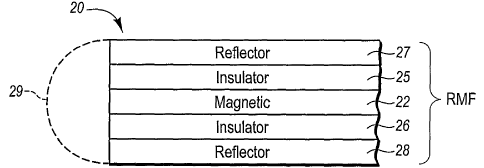
[032] Referring now to the drawings, wherein like structures are provided with
like
reference designations, Figure 1 depicts a reflective magnetic flake (RMF) 20
according to
one embodiment of the invention. The RMF 20 can be a generally symmetrical
thin film
structure comprising a magnetic layer 22, a first insulator layer 25 over one
major surface
of magnetic layer 22, and a second insulator layer 26 over an opposing second
major
surface of magnetic layer 22. A first reflector layer 27 is over first
insulator layer 25, and a
second reflector layer 28 is over second insulator layer 26.
[033] By inserting the insulator layer between the reflector layer and the
magnetic layer
galvanic corrosion of the flake is prevented. In addition, with the magnetic
layer located
between the outer reflector layers such as shown in Figure 1, the optical
properties of the
reflector layers are not degraded and the flake remains highly reflective.
[034] Flakes corresponding to RMF 20 can be formed by a web coating process
such as
described previously, in which the various layers are sequentially deposited
on a web
material to form a thin film structure, which is subsequently fractured and
removed from
the web to form a plurality of flakes. Alternatively, the first and second
reflector layers 27
and 28 can be formed as part of a contiguous reflecting layer 29 (shown in
phantom)
11
CA 02515587 2005-08-09
WO 2004/072186 PCT/IB2003/006263
substantially surrounding magnetic layer 22 and insulator layers 25 and 26,
which have
been previously formed by a web coating process.
[035] The RMF 20 can be used as a pigment flake or can be used as a core
section with
additional layers applied thereover such as in a color shifting pigment. In
the case of a
color shifting pigment, maintaining the high reflectivity of the reflector
layer is important
to preserve high brightness and chroma of the pigment. Each of the layers in
the coating
structure of RMF 20 is discussed hereafter in greater detail.
[036] The magnetic layer 22 can be composed of any magnetic or magnetizable
material, such as nickel, cobalt, iron, gadolinium, terbium, dysprosium,
erbium, and alloys
or oxides thereof. For example, a cobalt nickel alloy can be employed, with
the cobalt and
nickel having a ratio by weight of about 80% and about 20%, respectively. This
ratio for
each of these metals in the cobalt nickel alloy can be varied by plus or minus
about 10%
and still achieve the desired results. Thus, cobalt can be present in the
alloy in an amount
from about 70% to about 90% by weight, and nickel can be present in the alloy
in an
amount from about 10% to about 30% by weight. Other examples of alloys include
Fe/Si,
Ni/Fe (e.g., permalloy), Fe/Ni, Fe/Co, Fe/Ni/Mo, and combinations thereof.
Hard
magnetics of the type SmCo5, NdCo5, Sm2Co17, Nd2Fe14B, Sr6Fe2O3, TbFe2, Al-Ni-
Co, and
combinations thereof, can also be used as well as spinel ferrites of the type
Fe304,
NiFe2O4, MnFe2O4, CoFe2O4, or garnets of the type YIG (yttrium iron g arnet)
or GdIG
(gadolinium iron garnet), and combinations thereof.
[037] Although this broad range of magnetic materials can be used, the soft
magnets are
preferred in some embodiments of the invention. As used herein, the
terminology "soft
magnets" refers to any material exhibiting ferromagnetic properties but having
a
12
CA 02515587 2005-08-09
WO 2004/072186 PCT/1B2003/006263
remanence that is substantially zero after exposure to a magnetic force. Soft
magnets show
a quick response to an applied magnetic field, but have very low (coercive
fields (Hc) =
0.05-300 Oersteds (Oe)) or zero magnetic signatures, or retain very low
magnetic lines of
force after the magnetic field is removed. In addition, as used herein, the
terminology
"hard magnets" (also called permanent magnets) refers to any material that
exhibits
ferromagnetic properties and has a long lasting remanence after exposure to a
magnetizing
force. A ferromagnetic material is any material that has a penneability
substantially
greater than 1 and that exhibits magnetic hysteresis properties.
[038] The magnetic materials used to form magnetic layers in the flakes and
foils of the
invention preferably have a coercivity of less than about 2000 Oe, and more
preferably less
than about 300 Oe. Coercivity refers to the ability of a material to be
demagnetized by an
external magnetic field. The higher the value of coercivity, the higher the
magnetic field
required to demagnetize the material after the field is removed. In some
embodiments of
the invention, the magnetic layers used are preferably "soft" magnetic
materials (easily
demagnetized), as opposed to "hard" magnetic materials (difficult to
demagnetize) which
have higher coercivities. The coercivities of the foils, pigments or colorants
of the
magnetic color shifting designs according to the invention are preferably in a
range of
about 50 Oe to about 300 Oe. These coercivities are lower than in standard
recording
materials. Thus, embodiments of the invention that use soft magnets in
magnetic color
shifting pigments and magnetic non color shifting pigments are an improvement
over
conventional technologies. The use of soft magnetic materials in pigment
flakes allows for
easier dispersion of the flakes without clumping.
[039] The magnetic layer 22 can be formed to have a suitable physical
thickness from
13
CA 02515587 2005-08-09
WO 2004/072186 PCT/1B2003/006263
about 20 nm to about 3000 run, and preferably from about 50 nm to about 150
mn.
[040] The insulator layers 25 and 26 can be composed of any suitable
electrical
insulating material such as a dielectric material or some semiconductor
materials. For
example, the insulator layers can be composed of magnesium fluoride, aluminum
oxide,
nickel oxide, or combinations thereof, as well as any other insulating
material that is
suitable for use in thin film manufacturing processes and has the appropriate
electrical
insulating properties
[041] The insulator layers have an effective thickness for substantially
preventing
corrosion of the pigment flake by breaking an electrical path between the
metal reflector
layer (discussed hereafter) and the magnetic layer of the pigment flake. For
example, the
insulator layers can each have a physical thickness of at least about 10 nm,
and preferably
about 20 nm to about 40 nm.
[042] The reflector layers 27 and 28 can be composed of various reflective
materials.
Presently preferred materials are one or more metals, one or more metal
alloys, or
combinations thereof, because of their high reflectivity and ease of use,
although non-
metallic reflective materials can also be used. Nonlimiting examples of
suitable metallic
materials for the reflector layers include aluminum, silver, copper, gold,
platinum, tin,
titanium, palladium, nickel, cobalt, rhodium, niobium, chromium, iridium, and
combinations or alloys thereof. The reflector layers 24, 26 can be formed to
have a
suitable physical thickness from about 20 rim to about 1000 um, and preferably
from about
50 rim to about 100 nm.
[043] In an alternative embodiment of flake 20, an asymmetrical thin film
flake can be
provided that includes a thin film stack structure with the same layers as on
one side of
14
CA 02515587 2005-08-09
WO 2004/072186 PCT/IB2003/006263
magnetic layer 22 as shown in Figure 1. In such an embodiment, the
asymmetrical flake
includes magnetic layer 22, insulator layer 25 overlying magnetic layer 22,
and reflector
layer 27 overlying insulator layer 25. Each of these layers can be composed of
the same
materials and have the same thicknesses as described above for the
corresponding layers of
flake 20.
[044] In a further alternative embodiment, opposing dielectric layers may
optionally be
added to overlie reflector layers 27 and 28 of flake 20. These opposing
dielectric layers
add durability, rigidity, and corrosion resistance to flake 20. Alternatively,
an
encapsulating dielectric layer may be formed to substantially surround
reflector layers 27,
28 and magnetic layer 22. The dielectric layer(s) may be optionally clear, or
may be
selectively absorbing so as to contribute to the color effect of the pigment
flake. Examples
of suitable dielectric materials for such dielectric layers are described
hereafter with
respect to the embodiment of Figure 2.
[045] Figure 2 depicts a magnetic color shifting pigment flake 40 based upon a
RMF
according to another embodiment of the invention. The flake 40 is a generally
symmetrical multilayer thin film structure having coating layers over opposing
sides of a
RMF 42, which has a five-layer structure such as shown for the RMF in Figure
1. As
shown in Figure 2, a first dielectric layer 44 and a second dielectric layer
46 are
respectively over opposing sides of RMF 42. A first absorber layer 48 and a
second
absorber layer 50 are respectively over each of dielectric layers 44 and 46.
The RMF 42
can be formed from the same materials as discussed hereinabove for the RMF of
Figure 1,
while the dielectric and absorber layers of flake 40 are discussed hereafter
in greater detail.
[046] Flakes corresponding to flake 40 can be formed by a web coating process
such as
CA 02515587 2005-08-09
WO 2004/072186 PCT/1B2003/006263
described previously, in which the various layers of flake 40 are sequentially
deposited on
a web material to form a thin film structure, which is subsequently fractured
and removed
from the web to form a plurality of flakes.
[047] The dielectric layers 44 and 46 act as spacers in the thin film stack
structure of
flake 40. The dielectric layers are formed to have an effective optical
thickness for
imparting interference color and desired color shifting properties. The
dielectric layers
may be optionally clear, or may be selectively absorbing so as to contribute
to the color
effect of a pigment. The optical thickness is a well known optical parameter
defined as the
product rid, where i1 is the refractive index of the layer and d is the
physical thickness of
the layer. Typically, the optical thickness of a layer is expressed in terms
of a quarter wave
optical thickness (QWOT) that is equal to 4iid/k, where 7 is the wavelength at
which a
QWOT c ondition o ccurs. T he optical thickness o f t he dielectric 1 ayers
can r ange from
about 2 QWOT at a design wavelength of about 400 nm to about 9 QWOT at a
design
wavelength of about 700 nm, and preferably about 2-6 QWOT at 400-700 nm,
depending
upon the color shift desired. The dielectric layers can have a physical
thickness of about
100 nm to about 800 nm, and preferably about 140 nm to about 650 nm, depending
on the
color characteristics desired.
[048] Suitable materials for dielectric layers 44 and 46 include those having
a "high"
index of refraction, defined herein as greater than about 1.65, as well as
those have a "low"
index of refraction, which is defined herein as about 1.65 or less. Each of
the dielectric
layers can be formed of a single material or with a variety of material
combinations and
configurations. For example, the dielectric layers can be formed of only a low
index
16
CA 02515587 2005-08-09
WO 2004/072186 PCT/IB2003/006263
material or only a high index material, a mixture or multiple sublayers of two
or more low
index materials, a mixture or multiple sublayers of two or more high index
materials, or a
mixture or multiple sublayers of low index and high index materials. In
addition, the
dielectric layers can be formed partially or entirely of high/low dielectric
optical stacks,
which are discussed in further detail below. When a dielectric layer is formed
partially
with a dielectric optical stack, the remaining portion of the dielectric layer
can be formed
with a single material o r various material combinations and configurations a
s described
above.
[049] Examples of suitable high refractive index materials for dielectric
layers 44 and
46 include zinc sulfide (ZnS), zinc oxide (ZnO), zirconium oxide (Zr02),
titanium dioxide
(Ti02), diamond-like carbon, indium oxide (1n203), indium-tin-oxide (ITO),
tantalum
pentoxide (Ta205), ceric oxide (CeO2), yttrium oxide (Y203), europium oxide
(Eu203),
iron oxides such as (II)diiron(III) oxide (Fe304) and ferric oxide (Fe203),
hafnium nitride
(HfN), hafnium carbide (HfC), hafnium oxide (HfO2), lanthanum oxide (La203),
magnesium oxide (MgO), neodymium oxide (Nd203), praseodymium oxide .(Pr60ii),
samarium oxide (Sm203), antimony trioxide (Sb203), silicon monoxide (SiO),
selenium
trioxide (Se203), tin oxide (SnO2), tungsten trioxide (W03), combinations
thereof, and the
like.
[050] Examples of suitable low refractive index materials for dielectric
layers 44 and 46
include silicon dioxide (SiO2), aluminum oxide (A1203), metal fluorides such
as
magnesium fluoride (MgF2), aluminum fluoride (AIF3), cerium fluoride (CeF3),
lanthanum
fluoride (LaF3), sodium aluminum fluorides (e.g., Na3AIF6, Na5Al3F14),
neodymium
fluoride (NdF3), samarium fluoride (SmF3), barium fluoride (BaF2), calcium
fluoride
17
CA 02515587 2005-08-09
WO 2004/072186 PCT/IB2003/006263
(CaF2), lithium fluoride (LiF), combinations thereof, or any other low index
material
having an index of refraction of about 1.65 or less. For example, organic
monomers and
polymers can be utilized as low index materials, including dienes or alkenes
such as
acrylates (e.g., methacrylate), perfluoroalkenes, polytetrafluoroethylene
(Teflon),
fluorinated ethylene propylene (FEP), combinations thereof, and the like.
[0511 It should be appreciated that several of the above-listed dielectric
materials are
typically present in non-stoichiometric forms, often depending upon the
specific method
used to deposit the dielectric material as a coating layer, and that the above-
listed
compound names indicate the approximate stoichiometry. For example, silicon
monoxide
and silicon dioxide have nominal 1:1 and 1:2 silicon:oxygen ratios,
respectively, but the
actual silicon:oxygen ratio of a particular dielectric coating layer varies
somewhat from
these nominal values. Such non-stoichiometric dielectric materials are also
within the
scope of the present invention.
[052] As mentioned above, the dielectric layers can be formed of high/low
dielectric
optical stacks, which have alternating layers of low index (L) and high index
(H) materials.
When a dielectric layer is formed of a high/low dielectric stack, the color
shift at angle will
depend on the combined refractive index of the layers in the stack. Examples
of suitable
stack configurations for the dielectric layers include LH, HL, LHL, HLH, HLHL,
LHLH,
or in general (LHL)" or (HLH)", where n = 1-100, as well as various multiples
and
combinations thereof. In these stacks, LH, for example, indicates discrete
layers of a low
index material and a high index material.
[053] In an alternative embodiment, the high/low dielectric stacks are formed
with a
gradient index of refraction. For example, the stack can be formed with layers
having a
18
CA 02515587 2005-08-09
WO 2004/072186 PCT/IB2003/006263
graded index low-to-high, a graded index high-to-low, a graded index [low-to-
high-to-
low]", a graded index [high-to-low-to-high]", where n = 1-100, as well as
combinations and
multiples thereof. The graded index is produced by a gradual variance in the
refractive
index, such as low-to-high index or high-to-low index, of adjacent layers. The
graded
index of the layers can be produced by changing gases during deposition or co-
depositing
two materials (e.g., L and H) in differing proportions. Various high/low
optical stacks can
be used to enhance color shifting performance, provide antireflective
properties to the
dielectric layer, and change the possible color space of the pigments of the
invention.
[054] The dielectric layers 44 and 46 can each be composed of the same
material or a
different material, and can have the same or different optical or physical
thickness for each
layer. It will be appreciated that when the dielectric layers are composed of
different
materials or have different thicknesses, the flakes exhibit different colors
on each side
thereof and the resulting mix of flakes in a pigment or paint mixture would
show a new
color which is the combination of the two colors. The resulting color would be
based on
additive color theory of the two colors coming from the two sides of the
flakes. In a
multiplicity of flakes, the resulting color would be the additive sum of the
two colors
resulting from the random distribution of flakes having different sides
oriented toward the
observer.
[055] The absorber layers 48 and 50 of flake 40 can be composed of any
absorber
material having the desired absorption properties, including materials that
are uniformly
absorbing or non-uniformly absorbing in the visible part of the
electromagnetic spectrum.
Thus, selective absorbing (non-uniformly absorbing) materials or nonselective
absorbing
(uniformly absorbing) materials can be used, depending on the color
characteristics
19
CA 02515587 2005-08-09
WO 2004/072186 PCT/IB2003/006263
desired. For example, the absorber layers can be formed of nonselective
absorbing
metallic materials deposited to a thickness at which the absorber layer is at
least partially
absorbing, or semi-opaque.
[0561 Nonlimiting examples of suitable absorber materials include metallic
absorbers
such as chromium, aluminum, nickel, silver, copper, palladium, platinum,
titanium,
vanadium, cobalt, iron, tin, tungsten, molybdenum, rhodium, and niobium, as
well as their
corresponding oxides, sulfides, and carbides. Other suitable absorber
materials include
carbon, graphite, silicon, g ermanium, cermet, ferric oxide o r other metal
oxides, metals
mixed in a dielectric matrix, and other substances that are capable of acting
as a
nonselective or selective absorber in the visible spectrum. Various
combinations,
mixtures, compounds, or alloys of the above absorber materials may be used to
form the
absorber layers of flake 40.
[0571 Examples of suitable alloys of the above absorber materials include
Inconel (Ni-
Cr-Fe), stainless steels, Hastalloys (e.g., Ni-Mo-Fe; Ni-Mo-Fe-Cr; Ni-Si-Cu)
and titanium-
based alloys, such as titanium mixed with carbon (Ti/C), titanium mixed with
tungsten
(Ti/W), titanium mixed with niobium (Ti/Nb), titanium mixed with silicon
(Ti/Si), and
combinations thereof.
[0581 As mentioned above, the absorber layers can also be composed of an
absorbing
metal oxide, metal sulfide, metal carbide, or combinations thereof. For
example, one
preferred absorbing sulfide material is silver sulfide. Other examples of
suitable
compounds for the absorber layers include titanium-based compounds such as
titanium
nitride (TiN), titanium oxynitride (TiN,,Oy), titanium carbide (TiC), titanium
nitride
carbide (TiNXCZ), titanium oxynitride carbide (TiN,,OyCZ), titanium silicide
(TiSi2),
CA 02515587 2005-08-09
WO 2004/072186 PCT/IB2003/006263
titanium boride (TiB2), and combinations thereof. In the case of TiNXOy and
TiNXOYCZ,
preferably x = 0 to 1, y = 0 to 1, and z = 0 to 1, where x + y = 1 in TiNXOy
and x + y + z =
1 in TiNXOYCZ. For TiNXCZ, preferably x = 0 to 1 and z = 0 to 1, where x + z =
1.
Alternatively, the absorber layers can be composed of a titanium-based alloy
disposed in a
matrix of Ti, or can be composed of Ti disposed in a matrix of a titanium-
based alloy.
[059] It will be appreciated by one skilled in the art that the absorber
layers also can
also be formed from a magnetic material, such as a cobalt nickel alloy or
other magnetic
materials described previously. This simplifies the manufacture of the
magnetic color
shifting pigments by reducing the number of materials required.
[060] The absorber layers are formed to have a physical thickness in the range
from
about 3 nm to about 50 run, and preferably from about 5 nm to about 15 nm,
depending
upon the optical constants of the absorber layer material and the desired peak
shift. The
absorber layers can each be composed of the same material or a different
material, and can
have the same or different physical thickness for each layer.
[061] In an alternative embodiment of flake 40, an asymmetrical color shifting
flake
can be provided that includes a thin film stack structure with the same layers
as on one side
of RMF 42 as shown in Figure 2. Accordingly, the asymmetrical color shifting
flake
includes RMF 42, dielectric layer 44 overlying RMF 42, and absorber layer 48
overlying
dielectric layer 44. Each of these layers can be composed of the same
materials and have
the same thicknesses as described above for the corresponding layers of flake
40. In
addition, asymmetrical color shifting flakes can be formed by a web coating
process such
as described above in which the various layers are sequentially deposited on a
web material
to form a thin film structure, which is subsequently fractured and removed
from the web to
21
CA 02515587 2005-08-09
WO 2004/072186 PCT/IB2003/006263
form a plurality of flakes.
[062] . In a further alternative embodiment, flake 40 can be formed without
the absorber
layers. In this embodiment, opposing dielectric layers 44 and 46 are formed of
high/low
(H/L) dielectric optical stacks such as described previously. Thus, dielectric
layers 44 and
46 can be configured such that flake 40 has the coating structures: (HL)"
/RMF/(LH)",
(LH)"/RMF/(HL)", (LHL)" /RMF/(LHL)", (HLH)"/RMF/(HLH)n, or other similar
configurations, where n = 1-100 and the L and H layers are 1 quarterwave (QW)
at a
design wavelength.
[063] As a general rule, galvanic corrosion occurs between two metals if the
algebraic
difference of their atomic potentials in the Noble Metals Table is greater
than +/- 0.3 volts.
The potential of the aluminum/nickel pair is -1.41 V, indicating there is a
driving force for
galvanic corrosion of aluminum in a pigment having a seven-layer design, such
as
Cr/MgF2/Al/Ni/Al/MgF2/Cr, when the pigment is either immersed in an
electrolytic
solution or exposed to a humid environment. This seven-layer design pigment is
particularly sensitive to exposure in alkali or other basic solutions. To
reduce corrosion of
aluminum in such a pigment, the electrical contact between the dissimilar
metals Al and Ni
is eliminated by placing the insulator layers described herein between the
dissimilar
metals. In such a scheme, the design of the seven-layer pigment changes to a
to a nine-
layer pigment, such as shown in Figure 2, wherein the two insulator layers are
inserted
between the aluminum layer and the magnetic layer such as shown below:
Cr/MgF2/Al/MgF2 20 urn /Magnetic composite/ MgF2 20 nm /Al /MgF2ICr
[064] From a manufacturing convenience, the two insulator layers in this
embodiment
can be made from magnesium fluoride, which is a constituent component of the
dielectric
22
CA 02515587 2005-08-09
WO 2004/072186 PCT/1B2003/006263
layers of the pigment. Fabrication of the pigment with insulator layers of
MgF2 requires
two additional steps of rewinding the polyester roll (web) with a partially
coated
multilayered stack and deposition of the insulator layers of magnesium
fluoride. In an
alternative manufacturing scheme, the aluminum and magnetic layers can be
separated by
deposition of a 20 rim thick film of A1203 by reactive evaporation of aluminum
in the
presence of oxygen.
[065] In a further alternative manufacturing s cheme, the surface oft he first
reflector
layer such as aluminum is oxidized and the surface of the magnetic layer over
the oxidized
reflector layer is oxidized to thereby form oxide films between the dissimilar
metals. For
such a process, ion guns are installed downstream a short distance after the
aluminum
source but upstream from the source of a magnetic material. In this way, the
first
aluminum layer, being deposited from an aluminum source onto a first
dielectric layer
which has been deposited onto a first absorber layer, goes through an
oxidation zone where
its surface oxidizes to form a dense insulating film of aluminum oxide. The
oxygen
pressure, ion gun power, and the polyester roll rewinding speed are all
parameters used to
control the thickness of the A1203 film. In the next step, a magnetic material
(e.g., nickel)
is deposited on top of the insulating A1203 film. In the oxidation zone, a
dense NiO layer
forms on the surface of the magnetic material, thereby insulating the magnetic
layer from
the subsequent second aluminum layer. The NiO layer is a p-type semiconductor
that
provides electrical separation of the nickel layer and the second aluminum
layer. After
deposition of the second aluminum layer, a second dielectric layer such as a
magnesium
fluoride spacer is formed, followed by a second absorber layer such as a
chromium
absorber to complete the optical stack that has the following design:
23
CA 02515587 2005-08-09
WO 2004/072186 PCT/IB2003/006263
Substrate/Cr/MgF2/Al/A12O3/Ni/NiO/Al /MgF2 /Cr
[066] The thickness of insulating layers in the ion gun approach can be less
than about
20 nm because these layers have a higher density than films deposited by
thermal or
reactive evaporation. The advantage of such a process is that it is very
similar to the
process used in forming a seven-layer stack as far as the number of polyester
roll passes
through a coating machine, but the ion gun process generates a robust nine-
layer design
that is corrosion-resistant in humid environments and in electrolytic
solutions.
[067] Figure 3 depicts a reflective magnetic encapsulated (RME) flake 60
according to
another embodiment of the invention. The RME flake 60 has a three layer
coating
structure, with a reflector layer 62 substantially surrounding and
encapsulating an insulator
layer 63, which surrounds a core magnetic layer 64. The insulator layer 63
between
reflector layer 62 and magnetic layer 64 prevents galvanic corrosion of flake
60. In
addition, with the magnetic layer located within the outer reflector layer
such as shown in
Figure 3, the optical properties of the reflector layer is not degraded and
the reflector layer
remains highly reflective.
[068] The RME flake 60 can be used as a pigment particle, or can be used as a
core
particle with additional layers applied thereover. The reflector layer 62,
insulator layer 63,
and magnetic layer 64 can be composed of the same materials and can have the
same
thicknesses as discussed previously for the corresponding layers in flake 20.
[069] In an alternative embodiment of flake 60, a dielectric layer may
optionally be
added to overlie reflector layer 62, to add durability, rigidity, and
corrosion resistance to
flake 60. The dielectric layer may be optionally clear, or may be selectively
absorbing so
as to contribute to the color effect of the flake.
24
CA 02515587 2005-08-09
WO 2004/072186 PCT/1B2003/006263
[0701 Figure 4 depicts alternative coating structures (with phantom lines) for
a
magnetic color shifting pigment flake 80 in the form of an encapsulate based
upon either
the RMF or the RME flake discussed with respect to Figures 1 and 3. The flake
80 has a
magnetic core section 82 that is either a RMF or a RME flake, which can be
overcoated by
an encapsulating dielectric layer 84 substantially surrounding magnetic core
section 82.
An absorber layer 86, which overcoats dielectric layer 84, provides an outer
encapsulation
for flake 80. The hemispherical dashed lines on one side of flake 80 in Figure
4 indicate
that dielectric layer 84 and absorber layer 86 can be formed as contiguous
layers around
magnetic core section 82.
[0711 Alternatively, the magnetic core section 82 and dielectric layer can be
in the form
of a thin film core flake stack, in which opposing dielectric layers 84a and
84b are
preformed on the top and bottom surfaces but not on at least one side surface
of magnetic
core section 82 which is a RMF, with absorber layer 86 encapsulating the thin
film stack.
An encapsulation process can also be used to form additional layers on flake
80 such as a
capping layer (not shown). The pigment flake 80 exhibits a discrete color
shift such that
the pigment flake has a first color at a first angle of incident light or
viewing and a second
color different from the first color at a second angle of incident light or
viewing.
[072] In a further alternative embodiment, flake 80 can be formed without the
absorber
layer. In this embodiment, dielectric layer 84 is formed of contiguous
high/low (H/L)
dielectric optical coatings similar to the dielectric optical stacks described
previously.
Thus, dielectric layer 84 can have the coating structure (HL)", (LH)", (LHL)",
(HLH)", or
other similar configurations, where n = 1-100 and the L and H layers are 1 QW
at a design
wavelength.
CA 02515587 2011-06-03
10731 Various conventional coating processes can be utilized in forming the
dielectric and absorber layers by encapsulation. For example, suitable methods
for
forming the dielectric layer include vacuum vapor deposition, sol-gel
hydrolysis, CVD in
a fluidized bed, downstream plasma onto vibrating trays filled with particles,
and
electrochemical deposition. Suitable methods for forming the absorber layers
include
vacuum vapor deposition, and sputtering onto a mechanically vibrating bed of
particles,
such as disclosed in Patent No. US 6,241,858 B1. Alternatively, the absorber
coating may
be deposited by decomposition through pyrolysis of metal-organo compounds or
related
CVD processes which may be carried out in a fluidized bed. If no further
grinding is
carried out, these methods result in an encapsulated magnetic core with
dielectric and
absorber layers therearound. Various combinations of the above coating
processes may
be utilized during manufacture of pigment flakes with multiple encapsulating
coatings.
[0741 Various modifications and combinations of the foregoing embodiments are
also considered within the scope of the invention. For example, additional
dielectric,
absorber, and/or other optical coatings can be formed around each of the above
embodiments to yield further desired optical characteristics. Such additional
coatings can
provide further color effects to the pigments.
[0751 In addition, an optional transparent overlayer coating can be formed on
the
outer surface(s) of each of the foregoing pigment embodiments to improve
durability. For
example, Figure 2 depicts in phantom a first transparent overlayer coating 52
over
absorber layer 50, and a second transparent overlayer coating 54 over absorber
layer 48.
Figure 4 depicts in phantom an optional transparent overlayer coating 90
surrounding
absorber layer
26
CA 02515587 2011-06-03
86. The transparent overlayer coating can be composed of any suitable
transparent
material that imparts protection, such as the high index and low index
dielectric materials
discussed previously, as well as polymers such as acrylates and styrenes,
glassy materials
such as silicate and borosilicate glasses, or combinations thereof. The
transparent
overlayer coating can be formed to have a suitable physical thickness from
about 5 nm to
about 10 m, and preferably from about 100 nm to about 1 m.
[076] Additional flake embodiments that can be modified to include the
insulator
layer between a magnetic layer and a reflector layer as described herein are
disclosed in a
copending patent application Serial No. 09/844,261, filed on April 27, 2001,
and entitled
"Multi-layered Magnetic Pigments and Foils".
[0771 The pigment flakes of the present invention can be interspersed within a
pigment medium to produce a colorant composition that can be applied to a wide
variety
of objects or papers. The pigment flakes added to a medium produces a
predetermined
optical response through radiation incident on a surface of the solidified
medium.
Preferably, the pigment medium contains a resin or mixture of resins that can
be dried or
hardened by thermal processes such as thermal cross-linking, thermal setting,
or thermal
solvent evaporation, or by photochemical cross-linking.
[0781 Suitable pigment media include various polymeric compositions or organic
binders such as alkyd resins, polyester resins, acrylic resins, polyurethane
resins, vinyl
resins, epoxies, styrenes, and the like. Examples of suitable resins include
melamine,
acrylates such as methyl methacrylate, ABS (acrylonitrile butadiene styrene)
resins, ink
and paint formulations based on alkyd resins, and various mixtures thereof.
The pigment
27
CA 02515587 2005-08-09
WO 2004/072186 PCT/IB2003/006263
medium also preferably contains a solvent for the resin, such an organic
solvent or water.
The flakes combined with the pigment media produce a colorant composition that
can be
used directly as a paint, ink, or moldable plastic material. The colorant
composition can
also be utilized as an additive to conventional paint, ink, or plastic
materials.
[0791 In addition, the flakes can be optionally blended with various additive
materials
such as conventional pigment flakes, particles, or dyes of different hues,
chroma and
brightness to achieve the color characteristics desired. For example, the
flakes can be
mixed with other conventional pigments, either of the interference type or
noninterference
type, to produce a range of other colors. This preblended composition can then
be
dispersed into a polymeric medium such as a paint, ink, plastic or other
polymeric pigment
vehicle for use in a conventional manner. Examples of suitable additive
materials are
disclosed in copending application Serial No. 09/844,261 referenced
previously.
[0801 The magnetic color shifting flakes of the present invention are
particularly suited
for use in applications where colorants of high chroma and durability are
desired. By
using the magnetic color shifting flakes in a colorant composition, high
chroma durable
paint or ink can be produced in which variable color effects are noticeable to
the human
eye. The color shifting flakes of the invention have a wide range of color
shifting
properties, including large shifts in chroma (degree of color purity) and also
large shifts in
hue (relative color) with a varying angle of view. Thus, an object colored
with a paint
containing the color shifting flakes of the invention will change color
depending upon
variations in the viewing angle or the angle of the object relative to the
viewing eye.
[081] The pigment flakes of the invention can be easily and economically
utilized in
paints and inks which can be applied to various objects or papers, such as
motorized
28
CA 02515587 2005-08-09
WO 2004/072186 PCT/IB2003/006263
vehicles, currency and security documents, household appliances, architectural
structures,
flooring, fabrics, sporting goods, electronic packaging/housing, product
packaging, etc.
The color shifting flakes can also be utilized in forming colored plastic
materials, coating
compositions, extrusions, electrostatic coatings, glass, and ceramic
materials.
[082] Generally, the foils of the invention have a nonsymmetrical thin film
coating
structure, which can correspond to the layer structures on one side of an RMF
in any of the
above described embodiments related to thin film stack flakes. The foils can
be laminated
to various objects or can be formed on a carrier substrate. The foils of the
invention can
also be used in a hot stamping configuration where the thin film stack of the
foil is
removed from a release layer of a substrate by use of a heat activated
adhesive and applied
to a countersurface. The adhesive can be either coated on a surface of the
foil opposite
from the substrate, or can be applied in the form of a UV activated adhesive
to the surface
on which the foil will be affixed.
[083] Figure 5 depicts a coating structure of a color shifting foil 100 formed
on a
substrate 102, which can be any suitable material such as a flexible PET web,
carrier
substrate, or other plastic material. The foil 100 includes a magnetic layer
104 over
substrate 102, an insulator layer 106 over magnetic layer 104, a reflector
layer 108 over
insulator layer 106, a dielectric layer 110 over reflector layer 108, and an
absorber layer
112 over dielectric layer 110. The magnetic, insulator, reflector, dielectric,
and absorber
layers can be composed of the same materials and can have the same thicknesses
as
described previously for the corresponding layers in flakes 20 and 40.
[084] The foil 100 can be formed by a web coating process, with the various
layers as
described above sequentially deposited on a web by conventional deposition
techniques to
29
CA 02515587 2005-08-09
WO 2004/072186 PCT/IB2003/006263
form a thin film foil structure. The foil 100 can be formed on a release layer
of a web so
that the foil can be subsequently removed and attached to a surface of an
object. The foil
100 can also be formed on a carrier substrate, which can be a web without a
release layer.
[085] In addition, an optional transparent overlayer coating can be formed on
the foils
of the invention to improve durability. For example, Figure 5 depicts in
phantom a
transparent overlayer coating 114 over absorber layer 112. The transparent
overlayer
coating 114 can be composed of any suitable transparent materials that impart
protection,
such as the materials discussed previously with respect to the transparent
overlayer
coatings of the pigment embodiments of the invention, and can have the same
thickness
ranges as such coatings.
[086] Additional foil embodiments that can be modified to include the
insulator layer
between a magnetic layer and a reflector layer as described herein are
disclosed in
copending application Serial No. 09/844,261 referenced previously. Other
embodiments,
such as various optical articles with paired optically variable structures,
can utilize the
magnetic pigment flakes and foils of the invention. Such optical articles are
disclosed in
application Serial No. 09/844,261. Various uses for magnetic pigments and
foils are also
disclosed in application Serial No. 09/844,261.
[087] The following examples are given to illustrate the present invention,
and are not
intended to limit the scope of the invention.
CA 02515587 2005-08-09
WO 2004/072186 PCT/IB2003/006263
Example 1
[088] Different samples of bright color shifting pigment flakes with the same
thickness
of MgF2 and Cr, but with different thicknesses of an insulator layer, were
fabricated by
depositing thin film layers on a web. The thin film layers were stripped to
produce flakes
that were reduced in size to about 20 nm (average size of a single flake).
[089] The first sample pigment flake had a conventional five-layer design of
Cr/MgF2/Al/MgF2/Cr. The second sample pigment flake was magnetic and had a
seven-
layer design of Cr/MgF2/Al/Ni/A /MgF2/Cr. The third sample pigment flake was
magnetic
and had a nine-layer coating design of Cr/MgF2/Al/MgF2/Ni/MgF2/AI/MgF2/Cr. The
MgF2 insulator layers between the Al and Ni layers had a thickness of 16 nm.
The fourth
sample pigment flake had the same nine-layer coating design as the third
sample, except
that the MgF2 insulator layers between the Al and Ni layers had a thickness of
23 nm. The
fifth sample pigment flake had the same nine-layer coating design as the third
sample,
except that the MgF2 insulator layers between the Al and Ni layers had a
thickness of 25
rim. The sixth sample pigment flake was magnetic and had a nine-layer coating
design of
Cr/MgF2/AUA1203/Ni/A1203/AUMgF2/Cr. The A1203 insulator layers between the Al
and
Ni layers had a thickness of 20 urn.
Example 2
[090] A paint vehicle and ground pigments of the samples of Example 1 were
mixed in
the ratio of 9:1 to make paint samples. The paint samples were spread on
polyester sheets
with a blade. Dry 1" x 3" pieces of painted polyester were immersed in a 2 wt-
% water
solution of NaOH for 10 minutes. The color of each sample was measured before
and after
31
CA 02515587 2005-08-09
WO 2004/072186 PCT/IB2003/006263
the immersion test. The color difference AE was used for comparison of the
tested
samples. The color difference AE in the L*a*b* color space indicates the
degree of color
difference but not the direction and is defined by the equation:
AE = [(AL*)2 + (Aa*)2 +(Ab*)211/2
where AL*, Aa*, Ab* are differences in L*, a*, and b* values, respectively. A
larger AE
indicates a large color difference caused by degradation of the thin film
layers in the
pigment flakes. In this example, the AE is the color change as a result of the
exposure to
NaOH. Table 1 lists the color difference of all the tested paint samples.
Table 1
Sample Pigment design AE after NaOH
1 5 layer stack with no dissimilar metals 34.20
2 7 layer stack with no insulator layers 54.77
3 9 layer stack with 16 nm thick insulator layers of MgF2 59.93
4 9 layer stack with 23 rim thick insulator layers of MgF2 39.32
5 9 layer stack with 25 nm thick insulator layers of MgF2 31.34
6 9 layer stack with 20 nm thick insulator layers of A1203 34.00
[091] As shown in Table 1, samples 2 and 3 had a much larger AE after NaOH
immersion than samples 4-6 which had the thicker insulator layers. Samples 4-6
showed
color differences that were comparable to sample 1 which had no dissimilar
metals.
32
CA 02515587 2005-08-09
WO 2004/072186 PCT/IB2003/006263
[0921 The present invention may be embodied in other specific forms without
departing
from its spirit or essential characteristics. The described embodiments are to
be considered
in all respects only as illustrative and not restrictive. The scope of the
invention is,
therefore, indicated by the appended claims rather than by the foregoing
description. All
changes that come within the meaning and range of equivalency of the claims
are to be
embraced within their scope.
33