Note: Descriptions are shown in the official language in which they were submitted.
CA 02515724 2005-08-10
WO 2004/072335 PCT/US2004/004107
Devices Having Vertically-Disposed Nanofabric Articles and
Methods of Making the Same
Cross-Reference to Related Applications
[0001] This application claims priority under 35 U.S.C. ~ 119(e) to U.S.
Provisional Pat. Apl., Ser. No. 60/446,786, filed on February 12, 2003,
entitled
Electro-Mechanical Switches and Memory Cells Using Vertically-Disposed
Nanofabric Articles and Methods of Making the Same and to U.S. Pat. ApI. No.
601446,783, filed on February 12, 2003, entitled Electro-Mechanical Switches
and
Memory Cells Using Horizontally-Disposed Nanofabric Articles and Methods of
Making the Same, which are incorporated herein by reference in their entirety.
[0002] This application is a continuation-in-part and claims priority under 35
U.S.C. ~ 120 to the following applications which are expressly incorporated
herein by
reference in their entirety:
[0003] U.S. Pat. Apl. Ser. No. 09/915,093, filed on July 25, 2001, entitled
Electromechanical Memory Array Using Nanotube Ribbons and Method for Making
Same;
[0004] U.S. Pat. Apl. Ser. No. 10/033,323, filed on December 28, 2001,
entitled
Electromechanical Three-Trace Junction Devices.
[0005] U.S. Pat. Apl. Ser. No. 10/128,118, filed April 23, 2002, entitled
Nanotube
Films and Articles; and
CA 02515724 2005-08-10
WO 2004/072335 PCT/US2004/004107
2
[0006] U.S. Pat. Apl. Ser. No. 10/341,005, filed on January 13, 2003, entitled
Methods of Making Carbon Nanotube Films, Layers, Fabrics, Ribbons, Elements
and
Articles.
Techfiical Field
[0007] The present application relates to devices having vertically-disposed
and
other non-horizontally disposed nanofabric articles and to methods of making
the
same.
Background
[0008] Memory devices have been proposed which use nanoscopic wires, such as
single-walled carbon nanotubes, to form crossbar junctions to serve as
rnernory cells.
See WO 01/03208, Nanoscopic Wire-Based Devices, Arrays, and Methods of Their
Manufacture; and Thomas Rueckes et al., "Carbon Nanotube-Based Nonvolatile
Random Access Memory for Molecular Computing," Science, vol. 289, pp. 94-97, 7
July, 2000.) Hereinafter these devices are called nanotube wire crossbar
memories
(NTWCMs). Under these proposals, individual single-walled nanotube wires
suspended over other wires define memory cells. Electrical signals are written
to one
or both wires to cause them to physically attract or repel relative to one
another. Each
physical state (i.e., attracted or repelled wires) corresponds to an
electrical state.
Repelled wires are an open circuit junction. Attracted wires are a closed
state forming
a rectified junction. When electrical power is removed from the junction, the
wires
retain their physical (and thus electrical) state thereby forming a non-
volatile memory
cell.
[0009] The NTWCM proposals rely on directed growth or chemical self assembly
techniques to grow the individual nanotubes needed for the memory cells. These
techniques are now believed to be difficult to employ at commercial scales
using
CA 02515724 2005-08-10
WO 2004/072335 PCT/US2004/004107
modern technology. Moreover, they may contain inherent limitations such as the
length of the nanotubes that may be grown reliably using these techniques, and
it may
difficult to control the statistical variance of geometries of nanotube wires
so grown.
Improved memory cell designs are thus desired.
[0010] U.S. Patent Publication No. 2003-0021966 discloses, among other things,
electromechanical circuits, such as memory cells, in which circuits include a
structure
having electrically conductive traces and supports extending from a surface of
a
substrate. Nanotube ribbons are suspended by the supports that crcs~ the
~el~ctrically
conductive traces. Each ribbon comprises one or more nanotiibes. The ribbons
are
formed from selectively removing material from a layer or matted fabric of
nanotubes.
[0011] For example, as disclosed in U.S. Patent Application Publication No.
2003-0021966, a nanofabric may be patterned into ribbons, and the ribbons can
be
used as a component to create non-volatile electromechanical memory cells. The
ribbon is electromechanically-deflectable in response to electrical stimulus
of control
traces and/or the ribbon. The deflected, physical state of the ribbon may be
made to
represent a corresponding information state. The deflected, physical state has
non-
volatile properties, meaning the ribbon retains its physical (and therefore
informational) state even if power to the memory cell is removed. As explained
in
U.S. Patent Application Publication No. 2003-0124325, three-trace
architectures may
be used for electromechanical memory cells, in which the two of the traces are
electrodes to control the deflection of the ribbon.
CA 02515724 2005-08-10
WO 2004/072335 PCT/US2004/004107
Sufnfnary
[0012] The present invention provides new devices having vertically-disposed
nanofabric articles and methods of making same.
[0013] Under certain aspects of the invention, an electro-mechanical device,
includes a structure having a major horizontal surface and a channel formed
therein.
A conductive trace is in the channel; and a nanotube article vertically
suspended in the
channel, in spaced relation to a vertical wall of the channel. The article is
electro-
mechanically deflectable in a horizontal direction toward the conductive
trace.
[0014] Under another aspect of the invention, the vertically suspended extent
of
the nanotube article is defined by a thin film process.
[0015] Under another aspect of the invention, the vertically suspended extent
of
the nanotube article is about 50 nanometers or less.
[0016] Under another aspect of the invention, the nanotube article is clamped
with
a conducting material disposed in porous spaces between some nanotubes of the
nanotube article.
[0017] Under another aspect of the invention, the nanotube article is formed
from
a porous nanofabric.
[0018] Under another aspect of the invention, the nanotube article is
electromechanically deflectable into contact with the conductive trace and the
contact
is either a volatile state or non-volatile state depending on the device
construction.
[0019] Under other aspects of the invention, the vertically oriented device is
arranged into various forms of three-trace devices.
[0020] Under yet other aspects of the invention, the channel may be used for
multiple independent devices, or for devices that share a common electrode.
CA 02515724 2005-08-10
WO 2004/072335 PCT/US2004/004107
Brief Description of the Drawings
[0021] In the Drawing,
[0022] Figures lA-B are perspective and cross-sectional views of an exemplary
electromechanical switch;
[0023] Figures 2A-B are cross-sectional views of devices according to certain
embodiments of the invention;
[0024] Figures 3A-4C are cross-sectional diagrams of three-trace devices
according to certain embodiments of the invention;
[0025] Figures 5A-L illustrate an exemplary method of fabricating devices
according to certain embodiments of the invention;
[0026] Figure 6-10 are cross-sectional views of various alternative
embodiments
of the invention;
[0027] Figures 11A-B are cross-sectional views of an exemplary
electromechanical devices; and
[0028] Figures 12 and 13 are micrographs of a nanofabric that conforms to non-
planar surfaces; and
[0029] Figure 14 is an image of an exemplary nanofabric shown in perspective.
Detailed Description
[0030] Preferred embodiments of the invention provide new articles having non-
horizontally-disposed nanotube articles and provide methods of making same.
Some
embodiments provide improved ways of clamping or pinching suspended nanotube
articles to improve their performance and manufacturability. Other embodiments
provide electromechanical memory cells, which may be discrete or embedded.
Under
some embodiments, the discrete memory cells use new approaches to connect to
other
CA 02515724 2005-08-10
WO 2004/072335 PCT/US2004/004107
circuitry or cells, which lowers the resistivity of traces to the memory
cells. Still
other embodiments provide memory cells that have volatile information state
(i.e., the
information state is lost when power is interrupted). Some other embodiments
use
three-trace architectures analogous to those of U.S. Patent Application
Publication
No. 2003-0124325, in that a nanofabric article may be disposed between the
electrodes to cause the article to deflect toward or away from one electrode
or the
other. These embodiments may utilize a combination of volatile and non-
volatile
characteristics; for example, information state may be non-volatile, but the
device
may use a three-trace architecture in which the deflection of the nanotube
article may
be caused by a trace having volatile state characteristics.
[0031] Nanofabrics or ribbons, created by growth or application of individual
tubes have been shown to substantially conform to substrate surfaces, such as
a
surface of a semiconductor substrate. Preferred embodiments of the present
make
devices such as electro-mechanical switches and memory cells using nanofabrics
that
conform to a surface which is substantially perpendicular to a semiconductor
substrate
(i.e. the nanofabrics are vertically-oriented, relative to a horizontal
substrate).
Devices and fabrication techniques to develop such vertically-disposed devices
are
described below, and include the ability to form switches and memory cells
having
relatively short spans of vertically suspended nanofabric articles with
corresponding
reductions in gap heights. In some embodiments, this allows for the use of
smaller
device dimensions and lower electrical resistances (and corresponding
decreased
cycling times and increased speed, e.g., performance up 100 GHz or more).
Volatile
and non-volatile switches, and numerous types of devices, examples of which
are
CA 02515724 2005-08-10
WO 2004/072335 PCT/US2004/004107
provided for illustration, can be thus created. In certain preferred
embodiments, the
articles are substantially a monolayer of carbon nanotubes.
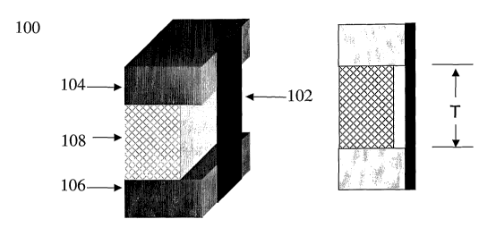
[0032] Figures lA-B are perspective and cross-sectional views of an exemplary
electromechanical switch. Structure 100 (Figure 1(A)) depicts an "off' state
and
structure 110 (Figure 1 (B)) depicts an "on" state. The designations "on" and
"off ' are
in some sense arbitrary, and this notation may be reversed with no loss of
generality.
In this embodiment, the structure contains nanofabric article 102 spanning
between an
upper insulating support structure 104 and a lower insulating support
structure 106.
Disposed between upper and lower insulating support structures 104 and 106 is
an
electrode 108.
[0033] Note that reference to a nanofabric, such as nanofabric article 102, is
generally meant to include any suitable structure or article comprising
nanotubes, and
specifically includes ribbons and nanofabric electrodes containing nanotubes.
[0034] Under certain preferred embodiments, a nanofabxic article 102 has a
span
T of less than about 180 nm or smaller and is pinned to insulating support
structures
104 and 106 (seen more clearly in figure 5L). The span of nanofabric will
depend on
deposition technique used, and under certain embodiments suspended spans can
be
shorter than lithographically-produced spans. The inventors envision vertical
spans as
small or smaller than 30nm. Pinning of nanofabric articles is described here
and
elsewhere in the incorporated references in more detail. The electrode 108 may
be
made of any suitable electrically conductive material and may be arranged in
any of a
variety of suitable geometries. Certain preferred embodiments utilize n-doped
silicon
to form such a conductive element which can be, preferably no wider than the
nanofabric article 102, e.g., about 180 nm or below. Other embodiments utilize
metal
CA 02515724 2005-08-10
WO 2004/072335 PCT/US2004/004107
as conductor. In certain embodiments the electrode 108 can be constructed from
a
nanofabric as well.
[0035] The material of the insulating support structures 104 and 106,
likewise,
may be made of a variety of materials and into various geometries, but certain
preferred embodiments utilize insulating material, such as spin-on-glass (SOG)
or
silicon nitride or silicon oxide.
[0036] As will be explained below, in certain embodiments, the nanofabric
article
102, as shown is held to the insulating support structures by friction. In
other
embodiments, the nanofabric article 102 may be held by other means, such as by
anchoring, stitching or pinning the nanofabric to the insulating support
structures
using any of a variety of techniques.
[0037] Specifically, the nanofabric article 102 may be coupled to another
material
by introducing a matrix material into the spaces between nanotubes in a porous
nanofabric to form a conducting composite junction, as described in the
references
incorporated above. Electrical and mechanical advantages may be obtained by
using
such composite junctions and connections. In one example, a conducting
material is
deposited onto the nanofabric and is allowed to penetrate into the spaces
within the
porous nanofabric, thus forming an improved electrical connection to the
nanofabric
and reduces contact resistance in the article. In another example, an
insulating
material is deposited onto the nanofabric and is allowed to penetrate into the
spaces
within the porous nanofabric, thus forming an improved mechanical pinning
contact
that increases reliability and manufacturability.
[0038] Evaporated or spin-coated material such as metals, semiconductors or
insulators especially - silicon, titanium, silicon oxide or polyamide - may be
used
CA 02515724 2005-08-10
WO 2004/072335 PCT/US2004/004107
to increase the pinning strength. The friction interaction can be increased
through the
use of chemical interactions, including covalent bonding through the use of
carbon
compounds such as pyrenes or other chemically reactive species. See R.J. Chen
et al.,
"Noncovalent Sidewall Functionalization of Single-Walled Carbon Nanotubes for
Protein Immobilization," J. Am. Chem. Soc., vol. 123, pp. 3838-39 (2001), and
Dai et
al., Appl. Phys. Lett., vol. 77, pp. 3015-I7 (2000), for exemplary techniques
for
pinning and coating nanotubes by metals. See also WO 01/03208 for techniques.
[0039] In some embodiments in which a nanofabric article 102 is spaced apart
from and crosses a corresponding, oppositely-disposed electrode, the
intersection
defines a memory or logic cell, switch or relay. More than one memory cell can
be
used in arrays or as individual or small groups of interconnected switches
depending
upon the application such as embedded memory, a two-chip memory device, relays
or
actuators. The actual number of such cells is immaterial to understanding the
invention, but the technology may support devices having information storage
capacities at least on the order of modern nonvolatile circuit devices.
[0040] Figures 2A-4C are cross-sectional diagrams of individual nanoswitches
illustrating various states of the device.
[0041] Figure 2A-B illustrate nanoswitches with different gap distances 202
and
208 between nanofabric article 102 and electrodes 204 and 210, respectively.
In
preferred embodiments, the vertical spacing between the insulating support
structures
104 and 106 is less than 180nm; this height is dependent upon the deposition
technique used. In the case of a switch with a 180 nm span of suspended
fabric, the
relative separation, i.e. gap distance 202, from the top of insulating support
structure
104 to the deflected position where the nanofabric article 102 attaches to
electrode
CA 02515724 2005-08-10
WO 2004/072335 PCT/US2004/004107
204 should be approximately 5-50 nm. In switches with smaller spans, the gap
would
likely also be smaller. The magnitude of the gap distance 202 is designed to
be
compatible with electromechanical switching capabilities of the memory device
or
other electronic application. The 5-50 nm gap distance is preferred for
certain
embodiments utilizing nanofabrics 102 made from carbon nanotubes, and reflects
the
specific interplay between strain energy and adhesion energy for the deflected
nanotubes. Other gap distances may be preferable for other materials.
Switching
between these states is accomplished by the application of specific voltages
across the
nanofabric article 102 and one or more of its associated electrodes, e.g. 204,
210.
Switching forces are based on the interplay of electrostatic attraction and
repulsion
between the nanofabric article 102 and the electrodes, e.g. 204, 210.
[0042] By selecting a gap distance 202 in which the strain energy is lower
than
the adhesion energy the nanofabric article 102 can remain in permanent "non-
volatile" contact with the electrode 204. If a larger gap distance 208 were
selected,
the strain energy increases to such an extent as to allow the nanofabric
article 102 to
contact the electrode 210 but not to remain in such contact without additional
power
input, defining a "volatile" condition. In some embodiments, such a volatile
switch is
preferred and can be combined with non-volatile switches as is necessary to
generate
particular electronic devices.
[0043] The dimensions given above are exemplary and non-limiting, and can be
greater or smaller in some embodiments, depending on the application and
materials
and techniques used. The length of the nanofabric article 102 in these and
other
vertically-disposed articles can be quite short in comparison to other types
of
nanofabric articles. In some cases, thin film techniques, such as thin film
deposition
CA 02515724 2005-08-10
WO 2004/072335 PCT/US2004/004107
11
or etching can be used rather than using lithographic techniques to form the
electrodes
and gaps spanned by the suspended nanofabric ribbons. In some embodiments the
suspended length can be shorter than the length of the nanofabrics used in
horizontally disposed devices, such as those in the incorporated reference
entitled
"Electro-Mechanical Switches and Memory Cells Using Horizontally-Disposed
Nanofabric Articles and Methods of Making the Same" (U.S. Provisional Pat.
Apl.
Ser. No. 60!446783), filed on February 12, 2003; filed on even date herewith
U.S.
Apl. Ser. No. yet to be assigned). The dependence on thin film deposition
rather than
lithographic patterning of the devices makes for more facile manufacturing.
[0044] A short span of nanofabric can lead to enhanced reliability and vastly
increased switching speeds up to 200 GHz for concomitantly lowered gap
heights.
Also, shorter spans of nanofabric result in reduced electrical resistance to
current
flowing through the nanofabric. Further embodiments, below, illustrate other
types of
vertically-disposed articles, and methods of manufacturing the same.
[0045] Figures 3A-C illustrate two possible "on" states of certain embodiments
of
the invention. When the device is as illustrated by 302 (Figure 3A, structure
300), the
nanofabric article 102 is separated from both electrodes 304 and 306 by a
distance
202. This state may be electrically detected in any of a variety of ways
described in
the foregoing references incorporated by reference. In this arrangement, an
"off ' state
corresponds to nanofabric-electrode junction being an open circuit, which may
be
sensed as such on either the nanofabric article 102 or electrode 304 when
addressed.
When the cell is as shown by 308 (Figure 3B, structure 310), the nanofabric
article
102 is deflected toward electrode 304. In certain embodiments the "on" states
corresponding to the nanofabric-electrode junction is an electrically
conducting,
CA 02515724 2005-08-10
WO 2004/072335 PCT/US2004/004107
12
rectifying junction (e.g., Schottky or PN), which may be sensed as such on
either the
nanofabric article 102 or electrode 306 when addressed. When the cell is as
shown by
312 (Figure 3C, structure 314), the nanofabric article 102 is deflected toward
electrode 306 generating an "on" state. The figures are not drawn to scale,
and the
distances 202, for example, need not be equal. Alternatively, one or the other
of the
electrodes may act as "set" electrode used alone or in combination with the
other
electrode to cause the nanotube article to deflect into contact with an
electrode, and
the other of the electrodes may act as a "release" electrode used alone or in
combination with the other electrode to cause the nanotube article to release
from
contact with the electrode.
[0046] Figures 4A-C illustrate some other possible tristate or tri-trace
device
configurations. A first tri-trace device 400 (Figure 4A) has two non-volatile
"on"
states. The distance 202 between the non-deflected nanofabric article 102 and
either
electrode 402 or 404 is small enough that upon deflection the nanofabric
contacts
either electrode 402 or 404. Under this embodiment a stable van der Waals
interaction is formed yielding a non-volatile condition in which the deflected
nanofabric article 102 contacts either electrode, closing a circuit and
remaining in
contact with the electrode indefinitely without the need for additional power.
[0047] A second tri-trace device 406 (Figure 4B) allows for nanofabric
deflection
to be either non-volatile or volatile. If the nanofabric article 102 deflects
toward
electrode 410, then the distance 202 is small enough to allow for a
nonvolatile state as
above. If, however the nanofabric article 102 is deflected toward electrode
408, then
the gap distance 208, between the nanofabric article 102 and the contacted
electrode
408 has been increased such that the strain energy of the stretched nanofabric
article
CA 02515724 2005-08-10
WO 2004/072335 PCT/US2004/004107
13
102 overcomes the van der Waals attraction between the nanofabric article 102
and
the electrode 408; the nanofabric article 102 briefly forms part of a closed
circuit
generating a transient "on" state and returns to its non-deflected, open
circuit state
generating an "off ' state.
[0048] Compare structure 400, which may be used as non-volatile switch, to
structure 406, which includes a volatile switch with gap 208. In structure 406
the gap
height 208 between the nanofabric and the electrode 408 has been increased
such that
the strain energy of the stretched nanofabric overcomes the van der Waals
attraction
between the fabric and the electrode. The nanofabric forms part of a closed
circuit
and returns to its non-deflected, open circuit state. It should be noted that
the effect of
the van der Waals interaction between nanofabrics and other elements can be
affected
at their interface(s). The effect may be enhanced or diminished; e.g., the
attractive
force can be diminished by coating the surface of the electrode with a thin
layer of
oxide or other suitable materials. A purpose of this diminishing of attractive
forces
may be to create volatile nanoswitches; such volatile switches may be
especially
useful in applications such as relays, sensors, transistors, etc.
[0049] Structure 412 (Figure 4C) illustrates yet a third tri-trace device
where the
gap distances 208 between the nanofabric article 102 and the electrodes 414
and 416
are large enough to form volatile nanoswitches as described above.
[0050] In certain embodiments involving a non-volatile cell, there is a high
ratio
between resistances in the "off ' and the "on" states. The differences between
resistances in the "off ' and "on" states provides a means to read which state
a
junction is in. In one approach, a "readout" current is applied to the
nanofabric or
electrode and the voltage across the junction is determined with a "sense
amplifier"
on the electrodes. Reads are non-destructive, meaning that the cell retains
its state,
CA 02515724 2005-08-10
WO 2004/072335 PCT/US2004/004107
14
and no write-back operations are needed as is required with semiconductor
DRAMS.
As alluded to above, the three-trace junctions of preferred embodiments bring
their
own advantages. By allowing for use of tristate memory cells, more information
may
be stored or represented by a given cell. Moreover, even if only one of the
"on" states
were used, three-trace junctions may increase switching speeds from the
ability to use
both conductive traces in concert to apply forces to move an
electromechanically
responsive nanofabric 102.
[0051] Among other things the structures as shown in Figures 3 and 4
(generally)
facilitate packaging and distribution, and allow the nanotube-technolagy cells
to be
more easily incorporated into other circuits and systems such as hybrid
circuits. The
vertical nature of the electrical architecture can also facilitate the
production of
stackable memory layers and the simplification of various interconnects.
Preferably,
the nanotube patch or segment is clamped (above and below) up to the portion
of the
nanofabric article that is so suspended. In addition, preferably, the
nanofabric article
is connected or joined to high conductivity signal paths.
[0052] One aspect of the present invention is directed to formation of
conductive
composite junctions whereby a suitable matrix material is disposed within and
around
the nanotubes or fibers of a nanofabric or other porous nano material. Such
junctions
can provide desirable mechanical andlor electrical properties. For example,
electrical
contact between a nanofabric and a metal connection or activation point may be
enhanced, or the contact resistance may be decreased by applying the metal
contact as
a matrix material impregnating the nanofabric tubes. Also, mechanical contact
and
strain may be increased as a result of the increased contact between the
nanotubes and
the matrix material.
[0053] Cross-sectional figures 5A-L, collectively, illustrate an exemplary
method
of fabricating a substantially vertical nano-electromechanical switch. By
vertical it is
CA 02515724 2005-08-10
WO 2004/072335 PCT/US2004/004107
meant that the switching element is substantially perpendicular to the major
surface of
the substrate. This aspect will be illustrated and described in detail below.
Certain
advantages can be realized in manufacturing such device using conformal
nanotube
andlor nanofabric materials. As a result, the length of the nanofabric article
can be
reduced in some embodiments by about two orders of magnitude. Additionally,
the
electrical resistance of a current-carrying nanofabric article is
substantially reduced
when the length of the article is reduced, as described herein.
[0054] In Figure 5A, a semiconductor substrate 501 coated with an insulating
layer 502 such as silicon dioxide or silicon nitride is provided. The
insulating layer
502 is preferably a few nanometers in thickness but could be as much 1 ~,m
thick
depending upon the electrical characteristics desired for different
applications. A
second layer 504 is deposited on insulating layer 502. Two non-exclusive
examples
of the material the second layer 504 can be made from are metals and
semiconductors;
the second layer having a top surface 506. A cavity 507 is defined in the
second layer
504. The cavity 507 can be created by reactive ion etching into the second
layer 504;
the cavity 507 is defined by inner walls 508 and an exposed top surface 510 of
insulating layer 502. Tn certain embodiments, a portion of second layer 504
remains
such that the bottom of the cavity 507 is conductive. Alternatively, an
insulating layer
502 could be provided to top surface 506 which could be etched to generate a
cavity.
The cavity 507 can be prefabricated as part of a trench or a via provided as
part of
preprocessing steps, e.g., as part of an overall integration scheme in
generation of an
electronic device.
[0055] Figure 5B illustrates a first insulating layer 512 made of silicon
nitride or
other material deposited on top of the exposed top surface 510 and top surface
506 to
CA 02515724 2005-08-10
WO 2004/072335 PCT/US2004/004107
16
generate top layer 514 of intermediate structure 516. According to one
embodiment,
the first insulating layer 512 is selectively etchable over polysilicon,
nanotubes and
silicon oxide or other selected insulator. A first insulating layer 512 which
will act as
a sacrificial layer to create a gap between subsequent layers can be in a
range of
thicknesses described below as shown in intermediate structure 516.
[0056] Figure 5C illustrates a monolayer of nanofabric 518 applied to
intermediate structure 516, forming intermediate structure 520. The nanofabric
518
may be applied by chemical vapor deposition, spin coating of suspensions of
nanotubes, aerosolized nanotube suspensions or dipping into a solution of
suspended
nanotubes.
[0057] Nanofabric layer 5I8 conforms to the underlying insulating layer 512
and
substantially follows the geometry of cavity 507. Examples of nanofabric
articles and
methods of manufacturing and using the same can be found in the previously-
mentioned and incorporated references. The resulting structure 520 thus
includes two
vertical portions 518A of the nanofabric 518 which is perpendicular to the
major
surface of the substrate 501. Devices created using these vertical portions
substantially parallel to channel 507 side walls .508, e.g. nano-switches, are
termed
"vertical" devices or switches.
[0058] Figure 5D illustrates a second insulating layer 522 applied over
nanofabric
518. Protective insulating layer 524 is deposited on top of second insulating
layer 522
having top surface 526, forming intermediate structure 528. The protective
insulating
layer 524 is not deposited on the side walls of the channel. The thickness of
protective insulating layer 524 can be, for example, on the order of 100 nm,
and a
non-exclusive example of the method of application of protective insulating
layer 524,
CA 02515724 2005-08-10
WO 2004/072335 PCT/US2004/004107
17
which may be an oxide layer, is by sputtering or high density plasma
deposition of
silicon dioxide. The optimal thickness is determined by the particular
application to
protect the layers below the insulating layer 524 from additional etching or
deposition
steps.
[0059] Figure 5E illustrates a polysilicon layer 530 deposited on top surface
526
of intermediate structure 528, filling the space between walls 508 in cavity
507.
Polysilicon layer 530 can be deposited to a height greater than that of top
surface 526
in order to get the proper amount of polysilicon layer into cavity 507,
creating an
overfilling condition as in intermediate structure 532. Polysilicon layer 530
is
subsequently planarized to etched polysilicon 534 with top surface 526 of
oxide layer
524 as is illustrated by intermediate structure 536 (Figure 5F).
[0060] Figure 5G illustrates polysilicon layer 534 etched to a first depth
538, by
any appropriate method. An exemplary method of creating such a depth is by
reactive
ion etch (RIE) as shown in intermediate structure 540; first depth 538 later
helps
define one edge of a suspended nanofabric segment. The thickness 541 of etched
polysilicon layer 534 is dependent on original trench depth 509; for example
the depth
may be in a range from 200 nm to 1 micron and for applications requiring
ultrahigh
speed electromechanical switches, the depth would preferably be below 200 nm.
This
depth can be reduced using thin film manufacturing techniques, as mentioned
elsewhere in this document and in the documents incorporated by reference.
[0061] Figure 5H illustrates a layer of oxide 542 deposited on exposed
surfaces of
intermediate structure 540. Horizontal portions 544 of oxide layer cover
trench walls
and vertical oxide layers 546 cover exposed, top surfaces of polysilicon layer
534.
CA 02515724 2005-08-10
WO 2004/072335 PCT/US2004/004107
18
Horizontal oxide layers 544 are removed, e.g., by oxide spacer etching,
leaving
intermediate structure 550 (Figure 5I).
[0062] Figure SJ illustrates polysilicon layer 534 etched to a second depth
552.
Second depth 552 may be approximately SOnm deeper than first depth 538. The
defined gap 554 allows exposure of regions of second insulating layer 522 as
is shown
in intermediate structure 556.
[0063] Since preferred nanofabrics are permeable or porous, the regions 512A
of
first insulating layer 512 below the regions of nanotube fabric 518A are
removable,
e.g. by wet etching. Removal of materials from beneath a porous nanofabric has
been
described by the present applicants in the patent references incorporated
above.
Suitable wet etching conditions to remove the layers of first insulating layer
512 and
second insulating Iayer 522 leave a suspended nanofabric 558 having vertical
height
560 as observed in intermediate structure 562 (Figure 5K). The wet etching may
leave an overhang owing to the nature of isotropic wet etching conditions.
Other
techniques such as dry etching may be utilized to provide an anisotropic
etching step.
[0064] The vertical height 560 is defined by the etching procedure. For a
vertical
height 560 of 200 nm the thicknesses of first insulating layer 512 and second
insulating Iayer 522 would be approximately 20 nrn in order to provide gap
distances
to create two non-volatile states. Smaller vertical gaps may be preferred in
certain
embodiments of the invention, e.g. 30nm gap heights.
[0065] Electrode material 566 is deposited into trench 507, leaving gaps 568
between electrode material 566 and suspended nanotube fabric 558 as shown in
intermediate structure 570 (Figure 5L).
CA 02515724 2005-08-10
WO 2004/072335 PCT/US2004/004107
19
[0066] The structure 570 illustrates a pair of vertically-suspended nanofabric
portions 572 surrounded by vertical gaps 574, 576 on either side of each
portion. The
structure may serve as a basis for a pair of bi- or tri-state switching
devices as is
explained below. The behavior of the switching devices is influenced by the
strain in
the suspended nanofabric portions and the surrounding gap distances, as
discussed
herein. Also, many configurations, including common electrode (e.g. 566)
configurations may be obtained using the structure 570. It is possible to
split structure
570 into two discrete sections (left, right) by a vertical divide running
vertically
through electrode 566 for example, leaving two bi- or tri-state switches that
can be
independently operated.
[0067] In these and other embodiments, the nature of the resulting devices and
switches depends on the construction and arrangement of the electrodes and
connections, among other factors. Attention is called to the construction of
various
types of electrodes in the following embodiments, as an indication of the
flexibility of
the design and concepts underlying these devices and the variety of their
potential
uses. For example, some devices share common electrodes between more than one
nanofabric article (e.g. two nanofabric switch elements being influenced by a
same
shared electrode). Other devices have separate electrodes that control the
behavior of
the nanofabric. One or more electrodes can be used with each nanofabric
article to
control the article, as mentioned in the incorporated reference entitled
"Electromechanical Three-Trace Junction Devices" (U.S. Pat. Apl. Ser. No.
10/033,323), filed on December 28, 2001.
[0068] If vertical height 560 is 200 nm and first insulating layer 512 and
second
insulating layer 522 are increased to a thickness of about 50 nm the nanotube
switch
CA 02515724 2005-08-10
WO 2004/072335 PCT/US2004/004107
of certain device types would become volatile at the necessary bias voltages
because
the deflected nanofabric has a strain energy higher than that of the van der
Waals
force keeping the fabric in contact with metallic region 504 or electrode 566.
The
thicknesses of first insulating layer 5I2 and second insulating layer 522 can
be
adjusted to generate either a non-volatile or volatile condition for a given
vertical gap
560 as called for by particular applications with desired electrical
characteristics.
[0069] Cross-sectional figure 6 illustrates an exemplary structure with
subsequent
layers of metallization. This structure includes electrode interconnect 602
and via 604
in contact with nanofabric 518, and a contiguous metallic layer 504
surrounding the
electromechanical switch both laterally and subjacently, as shown in
intermediate
structure 600.
[0070] Cross-sectional figure 7 illustrates an exemplary structure with
subsequent
layers of metallization. This structure is similar to intermediate structure
600 in
several respects. However, an insulating layer 702 separates the portions of
metallic
layers 504, and therefore metallic Iayer 504 does not surround the
electromechanical
switch elements, preventing crosstalk as shown in intermediate structure 600
[0071] Cross-sectional figure 8 illustrates an exemplary structure with
subsequent
layers of metallization. This structure is similar to intermediate structure
700.
However, the nanofabric Iayer 5I8 is not continuous, being split at the bottom
and
therefore there are two independent switches 802, 804, which have no
crosstalk, as
shown in intermediate structure 800.
[0072] Cross-sectional figure 9 is an exemplary structure with subsequent
layers
of metallization. This structure is similar to intermediate structure 800;
however,
instead of a single central electrode, there are two central electrodes, 902,
904
CA 02515724 2005-08-10
WO 2004/072335 PCT/US2004/004107
21
separated by insulating layer 906. Thus, intermediate structure 900 has two
nano-electromechanical switches, which can be operated independently.
[0073] Cross-sectional figure 10 is an exemplary structure with subsequent
layers
of metallization. This structure is similar to intermediate structures 800 and
900,
except there is no central electrode, at all. In this embodiment, it is
possible for the
nanofabric switches to contact metal layers 504 to make a volatile or non-
volatile
switch, and it is possible for the switches to contact one another so as to be
volatile or
non-volatile.
[0074] The devices and articles shown in the preceding embodiments are given
for illustrative purposes only, and other techniques may be used to produce
the same
or equivalents thereof. Furthermore, the articles shown may be substituted
with other
types of materials and geometries in yet other embodiments. For example,
rather than
using metallic electrodes, some embodiments of the present invention may
employ
nanotubes. In fact, devices comprising nanotube and nanofabric articles in
place of
the electrodes shown above can be constructed as well.
[0075] In certain embodiments it may be advantageous to utilize such
nanofabric
electrodes as contacts to portions of a transistor or as part of a transistor
or to contact
or become part of an interconnect for subsequent sense amplifier or addressing
logic
circuitry, see e.g. U.S. Pat. Apl. No. 10/379973 entitled, Hybrid Circuit
Having
Nanotube Electromechanical Memory.
[0076] Additional electrodes can provide extra control of a switch or device
constructed according to the present description. For example, Figure 6
includes two
distinct electrodes that will push and/or pull the vertical nanofabric
sections in unison.
CA 02515724 2005-08-10
WO 2004/072335 PCT/US2004/004107
22
The gap distances will determine whether the devices are volatile or
nonvolatile for a
given set of parameters.
[0077] Figure 7 includes 3 distinct electrodes and gives extra degrees of
freedom
(extra redundancy, extra information storage capability, etc.) to the devices.
Figure 8
also includes 3 electrodes.
[0078] Figure 9 includes 4 distinct electrodes, since the center electrode is
divided
into two electrodes (902, 904) by application of divider 906.
[0079] Figure 10 includes two electrodes on the sides of the channel, and uses
a
nanofabric section coupled to top electrode 602 as a third electrode in
structure 1000.
[0080] As mentioned previously, using vertically-disposed nanofabric articles
permits exploitation of the smaller dimensions achievable with thin film
technology
than with the lithographic techniques used in horizontally-disposed nanofabric
articles. For example, returning to Figure lA, the dimension T, or thickness
of the
electrode 108, across which the nanofabric is suspended is as little as a few
nm thick
(e.g. 10-100nm), and is formed using thin film techniques. As technology
develops in
this regard, the thickness T can be less than 10 nm thick. Therefore, the
scaling of the
dimensions tracks with thin film technology rather than scaling with
lithographic
technology. It should be noted that the gap distances used with reduced length
nanofabric articles may also be decreased accordingly.
[0081] Figures 11A-B illustrate an embodiment of the present invention having
an
oxidized electrode. Structure 1110 illustrates a nanofabric based switch
having an
insulation layer 1112 over the exposed surface of one electrode108.
(Fabrication of
such an oxidized electrode is explained in detail below. The insulation layer
1112
may be used to change the characteristics of the switch to be volatile or to
provide
CA 02515724 2005-08-10
WO 2004/072335 PCT/US2004/004107
23
further assurance of desired behavior. Figure 11B illustrates a structure
having
opposing electrodes with a nanofabric switch disposed between them. The
insulating
layer, placed on the facing surface of an opposing electrode may be used to
prevent
different fibers from the nanofabric element from simultaneously electrically
contacting both electrodes (304, 306) during a state transition. Such contact
may
prevent or hinder switching of the fabric between states.
[0082] Figures 12 and 13 are micrographs of exemplary conformal nanofabrics.
These figures illustrate how a fabric looks when formed and made to conform
over
vertical and horizontal surfaces.
[0083] The preferred embodiments are made using nanotube films, layers, or non-
woven fabrics so that they form, or may be made to form, various useful
patterned
components, elements or articles. (Herein "films," "layers," or "non-woven
fabrics"
are referred to as "fabrics" or "nanofabrics".) The components created from
the
nanofabrics retain desirable physical properties of the nanotubes and/or the
nanofabrics from which they are formed. In addition, preferred embodiments
allow
modern manufacturing techniques (e.g., those used in semiconductor
manufacture) to
be employed to utilize the nanofabric articles and devices.
[0084] Preferred embodiments of the present invention include articles and
methods that increase a strain in the nanofabrics, allowing selectable
construction of
volatile and non-volatile electro-mechanical switches, including tri-state or
tri-trace
switches having both volatile and non-volatile states. The nanofabrics in some
embodiments also provide for discrete cellular articles, such as memory cells,
to be
manufactured.
CA 02515724 2005-08-10
WO 2004/072335 PCT/US2004/004107
24
[0085] Figure 14 is an image of an exemplary fabric of nanotubes shown in
perspective. As can be seen, the fabric may be highly porous and appear as
several
threads with gaps in between. In this figure there are actually several
ribbons of
nanofabric extending from left to right separated from one another by areas
with no
nanotubes. One may notice that the fabric of figure 13 is likewise very porous
with a
few nanotubes spanning the channel and contacting electrodes. In both figures,
the
resolution of the figure is affected by the imaging technology so some
nanotubes may
not appear in focus or be noticeable.
[0086] It will be further appreciated that the scope of the present invention
is not
limited to the above-described embodiments but rather is defined by the
appended
claims, and that these claims will encompass modifications and improvements to
what
has been described.
What is claimed is: