Note: Descriptions are shown in the official language in which they were submitted.
CA 02516034 2005-08-16
-1-
APPARATUS AND PROCESS FOR REDUCING THE SUSCEPTIBILITY
OF ACTIVE IMPLANTABLE MEDICAL DEVICES TO MEDICAL
PROCEDURES SUCH AS MAGNETIC RESONANCE IMAGING
RELATED APPLICATIONS
[0001] This is a Continuation-in-Part of U.S. Patent Application Serial
No. 10/825,900 filed on April 15, 2004, the contents of which are incorporated
herein by reference. This is also a Continuation-in-Part of U.S. Patent
Application Serial No. 10/842,967, filed May 10, 2004. This application is
also
a Continuation-in-Part of U.S. Patent Application Serial No. 10/778,954, filed
February 12, 2004. . This application also claims priority from U.S.
Provisional
Application Serial No. 60/607,276, filed September 2, 2004.
BACKGROUND OF THE INVENTION
[0002] This invention relates generally to EMI filter assemblies,
particularly of the type used in active implantable medical devices (AIMDs)
such as cardiac pacemakers, cardioverter defibrillators and the like, which
decouple and shield internal electronic components of the medical device
from undesirable electromagnetic interference (EMI) signals.
[0003] Compatibility of cardiac pacemakers, implantable defibrillators
and other types of active implantable medical devices with magnetic
resonance imaging (MRI) and other types of hospital diagnostic equipment
has become a major issue. If one goes to the websites of the major cardiac
pacemaker manufacturers in the United States, which include St. Jude
Medical, Medtronic and Guidant, one will see that the use of MRI is generally
contra-indicated with pacemakers and implantable defibrillators. See also
"Safety Aspects of Cardiac Pacemakers in Magnetic Resonance Imaging", a
dissertation submitted to the Swiss Federal Institute of Technology Zurich
presented by Roger Christoph Luchinger. "Dielectric Properties of Biological
Tissues: I. Literature Survey", by C. Gabriel, S. Gabriel and E. Cortout;
"Dielectric Properties of Biological Tissues: II. Measurements and the
Frequency Range 0 Hz to 20 GHz", by S. Gabriel, R.W. Lau and C. Gabriel;
"Dielectric Properties of Biological Tissues: III. Parametric Models for the
GREATB-47387
UTILITY APP
FILED 3/31/05
CA 02516034 2005-08-16
-2-
Dielectric Spectrum of Tissues", by S. Gabriel, R.W. Lau and C. Gabriel; and
"Advanced Engineering Electromagnetics, C.A. Balanis, Wiley, 1989, all of
which are incorporated herein by reference.
[0004] However, an extensive review of the literature indicates that
MRI is indeed often used with pacemaker patients. The safety and feasibility
of MRI in patients with cardiac pacemakers is an issue of gaining
significance.
The effects of MRI on patients' pacemaker systems have only been analyzed
retrospectively in some case reports. There are a number of papers that
indicate that MRI on new generation pacemakers can be conducted up to 0.5
Tesla (T). MRI is one of medicine's most valuable diagnostic tools. An
absolute contra-indication for pacemaker patients means that pacemaker and
ICD wearers are excluded from MRI. This is particularly true of scans of the
thorax and abdominal areas. Because of MRI's incredible value as a
diagnostic tool for imaging organs and other body tissues, many physicians
simply take the risk and go ahead and perform MRI on a pacemaker patient.
The literature indicates a number of precautions that physicians should take
in
this case, including limiting the power of the MRI magnetic field, programming
the pacemaker to fixed or asynchronous pacing mode (activation of the reed
switch), and then careful reprogramming and evaluation of the pacemaker
and patient after the procedure is complete. There have been reports of
latent problems with cardiac pacemakers after an MRI procedure occurring
many days later.
[0005] There are three types of electromagnetic fields used in an MRI
unit. The first type is the main static magnetic field which is used to align
protons in body tissue. The field strength varies from 0.5 to 1.5 Tesla in
most
of the currently available MRI units in clinical use. Some of the newer MRI
system fields can go as high as 4 to 5 Tesla. This is about 100,000 times the
magnetic field strength of the earth. A static magnetic field can induce
powerful mechanical forces on any magnetic materials implanted within the
patient. This would include certain components within the cardiac pacemaker
itself and or leadwire systems. It is not likely (other than sudden system
shut
down) that the static MRI magnetic field can induce currents into the
pacemaker leadwire system and hence into the pacemaker itself. It is a basic
principle of physics that a magnetic field must either be time-varying as it
cuts
GREATB-47387
UTILITY APP
FILED 3/31/05
CA 02516034 2005-08-16
-3-
across the conductor, or the conductor itself must move within the magnetic
field for currents to be induced. The lossy ferrite inductor or toroidal slab
concept as described herein is not intended to provide protection against
static magnetic fields such as those produced by magnetic resonance
imaging.
[0006] The second type of field produced by magnetic resonance
imaging is the pulsed RF field which is generated by the body coil or head
coil. This is used to change the energy state of the protons and illicit MRI
signals from tissue. The RF field is homogeneous in the central region and
has two main components: (1 ) the magnetic field is circularly polarized in
the
actual plane; and (2) the electric field is related to the magnetic field by
Maxwell's equations. In general, the RF field is switched on and off during
measurements and usually has a frequency of 21 MHz to 64 MHz to 128 MHz
depending upon the static magnetic field strength.
[0007] The third type of electromagnetic field is the time-varying
magnetic gradient fields which are used for spatial localization. These change
their strength along different orientations and operating frequencies on the
order of 1 kHz. The vectors of the magnetic field gradients in the X, Y and Z
directions are produced by three sets of orthogonally positioned coils and are
switched on only during the measurements.
[0008] Feedthrough terminal pin assemblies are generally well known
in the art for use in connecting electrical signals through the housing or
case
of an electronic instrument. For example, in implantable medical devices such
as cardiac pacemakers, defibrillators and the like, the terminal pin assembly
comprises one or more conductive terminal pins supported by an insulator
structure for feedthrough passage of electrical signals from the exterior to
the
interior of the medical device. Many different insulator structures and
related
mounting methods are known for use in medical devices wherein the insulator
structure provides a hermetic seal to prevent entry of patient body fluids
into
the medical device housing, where such body fluids could otherwise interfere
with the operation of and/or cause damage to internal electronic components
of the medical device.
[0009] In the past, two primary technologies have been employed to
manufacture the hermetic seal. One technique involves the use of an alumina
GREATB-47387
UTILITY APP
FILED 3/31/05
CA 02516034 2005-08-16
-4-
insulator which is metallized to accept brazing material. This alumina
insulator
is brazed to the terminal pin or pins, and also town outer metal ferrule of
titanium or the like. The alumina insulator supports the terminal pin or pins
in
insulated spaced relation from the ferrule which is adapted for suitable
mounting within an access opening formed in the housing of the medical
device. In an alternative technique, the hermetic seal comprises a glass-
based seal forming a compression or matched fused glass seal for supporting
the terminal pin or pins within an outer metal ferrule.
[0010] The feedthrough terminal pins are typically connected to one
or more leadwires which, in the example of a cardiac pacemaker, sense
signals from the patient's heart and also couple electronic pacing pulses from
the medical device to the patient's heart. Unfortunately, these leadwires can
act as an antenna to collect stray electromagnetic interference (EMI) signals
for transmission via the terminal pins into the interior of the medical
device.
Such unwanted EMI signals can disrupt proper operation of the medical
device, resulting in malfunction or failure. For example, it has been
documented that stray EMI signals emanating from cellular telephones can
inhibit pacemaker operation, resulting in asynchronous pacing, tracking and
missed beats. To address this problem, hermetically sealed feedthrough
terminal pin assemblies have been designed to include a feedthrough
capacitor for decoupling EMI signals in a manner preventing such unwanted
signals from entering the housing of the implantable medical device. See, for
example, U.S. Patent Nos. 4,424,551; 5,333,095; 5,751,539; 5,905,627;
5,973,906; 6,008,980; and 6,566.978. These prior art feedthrough capacitor
EMI filters generally provide a high degree of attenuation to EMI in the
frequency range between 450 and 3000 MHz.
[0011] While feedthrough capacitor filter assemblies have provided a
significant advance in the art, a remaining area of concern is powerful low
frequency emitters like MRI. As previously mentioned, feedthrough
capacitors, as described in the prior art, work by providing a low impedance
to
ground (the overall electromagnetic shield of the implantable medical device)
thereby by-passing such high frequency signals before they can enter and
disrupt sensitive pacemaker electronic circuitry. However, when a pacemaker
leadwire system is exposed to a powerful time varying electromagnetic field,
GREATB-47387
UTILITY APP
FILED 3/31/05
CA 02516034 2005-08-16
-5-
such as induced by MRI, the last thing that is desirable is to create a low
impedance in the leadwire system. Low impedance in the leadwire system
only increases the current that would flow in the leads thereby creating
additional leadwire heating and/or myocardial tissue necrosis at the
pacemaker TIP to RING interface. Accordingly, it would be desirable to
actually raise the impedance of the leadwire system at certain critical
frequencies thereby reducing the undesirable currents in the leadwire system.
[0012] It is instructive to note how voltages and EMI are induced into
an implanted leadwire system. At very low frequency (VLF), voltages are
induced at the input to the cardiac pacemaker as currents circulate throughout
the patient's body. Because of the vector displacement between the
pacemaker can and, for example, the TIP electrode, voltage drop across body
tissues may be sensed due to Ohms Law and the circulating RF signal. At
higher frequencies, the implanted leadwire systems actually act as antennas
where currents are induced along their length. These antennas are not very
efficient due to the damping effects of body tissue; however, this can often
be
offset by body resonances. At very high frequencies (such as cellular
telephone frequencies), EMI signals are induced only into the first area of
the
leadwire system (for example, at the header block of a cardiac pacemaker).
This has to do with the wavelength of the signals involved and where they
couple efficiently into the system. Magnetic field coupling into an implanted
leadwire system is based on loop areas. For example, in a cardiac
pacemaker, there is a loop formed by the leadwire as it comes from the
cardiac pacemaker housing to its distal TIP located in the right ventricle.
The
return path is through body fluid and tissue generally straight from the TIP
electrode in the right ventricle back up to the pacemaker case or housing.
This forms an enclosed area which can be measured from patient X-rays in
square centimeters. The inventor has participated with the Association for the
Advancement of Medical Instrumentation (AAMI) through their Committee
PC69, which is chaired by Mitchell Shein of the United States Food and Drug
Administration (FDA). This committee is known as the Pacemaker EMC Task
Force. One of the recent accomplishments of this committee was to visit
various pacemaker centers around the United States and to trace patient X-
rays and actually measure these loop areas. The report was recently issued
GREATB-47387
UTILITY APP
FILED 3/31/05
CA 02516034 2005-08-16
-6-
which indicates that the average loop area is 200 to 225 square centimeters.
This is an average and is subject to great statistical variation. For example,
in
a large adult patient with an abdominal implant, the implanted loop area is
much larger (greater than 450 square centimeters).
[0013] Relating now to the specific case of MRI, the magnetic
gradient fields would be induced through enclosed loop areas. However, the
pulsed RF fields, which are generated by the body coil, would also be induced
into the leadwire system by antenna action.
[0014] There are a number of potential problems with MRI, including:
(1 ) Closure of the pacemaker reed switch. When a pacemaker is
brought close to the MRI scanner, the reed switch can close, which puts the
pacemaker into a fixed rate or asynchronous pacing mode. Asynchronous
pacing may compete with the patient's underlying cardiac rhythm. This is one
reason why patients have generally been advised not to undergo MRI. Fixed
rate or asynchronous pacing for most patients is not an issue. However, in
patients with unstable conditions, such as myocardial ischemia, there is a
substantial risk for ventricular fibrillation during asynchronous pacing. In
most
modern pacemakers the magnetic reed switch function is programmable. If
the magnetic reed switch response is switched off, then synchronous pacing
is still possible even in strong magnetic fields. The possibility to open and
re-
close the reed switch in the main magnetic field by the gradient field cannot
be excluded. However, it is generally felt that the reed switch will remain
closed due to the powerful static magnetic field. It is theoretically possible
for
certain reed switch orientations at the gradient field to be capable of
repeatedly closing and re-opening the reed switch.
(2) Reed switch damage. Direct damage to the reed switch is
theoretically possible, but has not been reported in any of the known
literature. In an article written by Roger Christoph Luchinger of Zurich, he
reports on testing in which reed switches were exposed to the static magnetic
field of MRI equipment. After extended exposure to these static magnetic
fields, the reed switches functioned normally at close to the same field
strength as before the test.
(3) Pacemaker displacement. Some parts of pacemakers, such as the
batteries and reed switch, contain ferrous magnetic materials and are thus
GREATB-47387
UTILITY APP
FILED 3/31/05
CA 02516034 2005-08-16
-7-
subject to mechanical forces during MRI. Pacemaker displacement may
occur in response to magnetic force or magnetic torque.
(4) Radio freguency field. At the frequencies of interest in MRI, RF
energy can be absorbed and converted to heat. The power deposited by RF
pulses during MRI is complex and is dependent upon the power and duration
of the RF pulse, the transmitted frequency, the number of RF pulses applied
per unit time, and the type of configuration of the RF transmitter coil used.
The amount of heating also depends upon the volume of tissue imaged, the
electrical resistivity of tissue and the configuration of the anatomical
region
imaged. The cause of heating in an MRI environment is two fold: (a) RF field
coupling to the lead can occur which induces significant local heating; and
(b)
currents induced during the RF transmission can cause local Ohms Law
heating next to the distal TIP electrode of the implanted lead. The RF field
in
an MRI scanner can produce enough energy to induce leadwire currents
sufficient to destroy some of the adjacent myocardial tissue. Various ablation
has also been observed. The effects of this heating are not readily detectable
by monitoring during the MRI. Indications that heating has occurred would
include an increase in pacing threshold, myocardial perforation and lead
penetration, or even arrhythmias caused by scar tissue. Such long term
heating effects of MRI have not been well studied yet.
(5) Alterations of pacing rate due to the applied radio freauency field. It
has been observed that the RF field may induce undesirable fast pacing (QRS
complex) rates. There are two mechanisms which have been proposed to
explain rapid pacing: direct interference with pacemaker electronics or
pacemaker reprogramming (or reset). In both of these cases, it would be
desirable to raise the impedance, make the feedthrough capacitor more
effective and provide a very high degree of protection to AIMD electronics.
This will make alterations in pacemaker pacing rate and/or pacemaker
reprogramming much more unlikely.
(6) Time-varying magnetic Gradient fields. The contribution of the time-
varying gradient to the total strength of the MRI magnetic field is
negligible,
however, pacemaker systems could be affected because these fields are
rapidly applied and removed. The time rate of change of the magnetic field is
directly related to how much electromagnetic force and hence current can be
GREATB-47387
UTILITY APP
FILED 3/31/05
CA 02516034 2005-08-16
_$_
induced into a leadwire system. Luchinger reports that even using today's
gradient systems with a time-varying field up to 50 Tesla per second, the
induced currents are likely to stay below the biological thresholds for
cardiac
fibrillation. A theoretical upper limit for the induced voltage by the time-
s varying magnetic gradient field is 20 volts. Such a voltage during more than
0.1 milliseconds could be enough energy to directly pace the heart.
(7) Heating. Currents induced by time-varying magnetic gradient fields
may lead to local heating. Researchers feel that the calculated heating effect
of the gradient field is much less as compared to that caused by the RF field
and therefore may be neglected.
(0015] There are additional problems possible with implantable
cardioverter defibrillators (ICDs). ICDs use different and larger batteries
which could cause higher magnetic forces. The programmable sensitivity in
ICDs is normally much higher than it is for pacemakers, therefore, ICDs may
falsely detect a ventricular tachyarrhythmia and inappropriately deliver
therapy. In this case, therapy might include anti-tachycardia pacing, cardio
version or defibrillation (high voltage shock) therapies. MRI magnetic fields
may prevent detection of a dangerous ventricular arrhythmia or fibrillation.
There can also be heating problems of ICD leads which are expected to be
comparable to those of pacemaker leads. Ablation of vascular walls is
another concern.
[0016] In summary, there are a number of studies that have shown
that MRI patients with active implantable medical devices, such as cardiac
pacemakers, can be at risk for potential hazardous effects. However, there
are a number of anecdotal reports that MRI can be safe for extremity imaging
of pacemaker patients (only when an MRI is thought to be an absolute
diagnostic necessity). The effect of an MRI system on the function of
pacemakers and ICDs depends on various factors, including the strength of
the static magnetic field, the pulse sequence (gradient and RF field used),
the anatomic region being imaged, and many other factors. Further
complicating this is the fact that each manufacturer's pacemaker and ICD
designs behave differently. Most experts still conclude that MRI for the
pacemaker patient should not be considered safe. Paradoxically, this also
does not mean that the patient should not receive MRI. The physician must
GREATB-47387
UTILITY APP
FILED 3/31/05
CA 02516034 2005-08-16
_g_
make an evaluation given the pacemaker patient's condition and weigh the
potential risks of MRI against the benefits of this powerful diagnostic tool.
As
MRI technology progresses, including higher field gradient changes over time
applied to thinner tissue slices at more rapid imagery, the situation will
continue to evolve and become more complex. An example of this paradox
is a pacemaker patient who is suspected to have a cancer of the lung.
Treatment of such a tumor may require stereotactic imaging only made
possible through fine focus MRI. With the patient's life literally at risk,
the
physician may make the decision to perform MRI in spite of all of the
previously described attendant risks to the pacemaker system.
[0017] It is clear that MRI will continue to be used in patients with an
implantable medical device. There are a number of other hospital
procedures, including electrocautery surgery, lithotripsy, etc., to which a
pacemaker patient may also be exposed. Accordingly, there is a need for
circuit protection devices which will improve the immunity of active
implantable medical device systems to diagnostic procedures such as MRI.
There is also a need to provide increased filtering for AIMD's due to the
recent
proliferation in the marketplace of new higher power emitters. These include
aftermarket cellular telephone amplifiers, associated higher gain antennas
and radio frequency indentification (RFID) readers and scanners. The
present invention fulfills all of these needs and provides other related
advantages.
SUMMARY OF THE INVENTION
[0018] The present invention resides in a feedthrough terminal
assembly for an active implantable medical device (AIMD) including a plurality
of leadwires extending from electronic circuitry of the AIMD, and a Iossy
ferrite
inductor through which the leadwires extend in non-conductive relation for
increasing the impedance of the leadwires at selected RF frequencies and
reducing magnetic flux core saturation of the lossy ferrite inductor through
phase cancellation of signals carried by the leadwires. The present invention
also resides in a process for filtering electromagnetic interference (EMI) in
an
implanted leadwire extending from an active implantable medical device
GREATB-47387
UTILITY APP
FILED 3/31/05
CA 02516034 2005-08-16
-10-
(AIMD) into body fluids or tissue, wherein the leadwire is subjected to
occasional high-power electromagnetic fields such as those produced by
medical diagnostic equipment including magnetic resonance imaging. In the
process of the present invention, the leadwire is passed through an inductive
and resistive low pass filter element to increase EMI protection of AIMD
electronics and to raise the output impedance of the AIMD circuitry thereby
reducing currents induced in the implanted leadwire by the occasional high-
power electromagnetic fields, wherein the low pass filter element has a
diameter-to-thickness ratio of at least 1:1.
[0019] Both the feedthrough terminal assembly and related process
are specifically designed for use with active implantable medical devices
including a cardiac pacemaker, an implantable defibrillator, a congestive
heart
failure device, a hearing implant, a neurostimulator, a drug pump, a
ventricular
assist device, an insulin pump, a spinal cord stimulator, an implantable
sensing system, an artificial heart, an incontinence device, a bone growth
stimulator, a gastric pacemaker, or a prosthetic device.
[0020] In the novel feedthrough terminal assemblies described
herein, the leadwires may comprise a first leadwire extending from the
electronic circuitry of the AIMD through a housing of the AIMD to a point
within a human body. A second leadwire may be conductively coupled to at
least a portion of the AIMD housing and the AIMD circuitry. A conformal
coating is provided over the lossy ferrite inductor, which coating preferably
comprises Paralene C, D, E or N.
[0021] In several embodiments, an insulator is disposed between the
lossy ferrite inductor and the leadwires. One or more additional lossy ferrite
inductors may be provided through which the leadwires extend in non-
conductive relation. The lossy ferrite inductors may be disposed adjacent to
one another and each can be comprised of materials having different physical
or electrical properties. When a hermetic insulator is disposed between the
leadwires and the ferrule, the lossy ferrite inductors may be disposed on
opposite sides of the insulator.
[0022] Advantageously, the lossy ferrite inductor may be bonded to
the insulator to form a beam-like structure. Moreover, the lossy ferrite
GREATB-47387
UTILITY APP
FILED 3/31/05
CA 02516034 2005-08-16
-11-
inductor may include an aperture through which a leak detection gas can be
detected.
[0023] In several embodiments, leadwires are wound around the
lossy ferrite inductor to form multiple turns. Adjacent portions of the wound
leadwire are electrically insulated from one another. The lossy ferrite
inductor
may further include a notch for receiving the wound leadwire. Further, the
lossy ferrite inductor may include multiple notches therein. At least two
leadwires may be wound about the lossy ferrite inductor to form one or more
turns, and the turn count for the leadwires need not be equal.
[0024] Means are also provided for maintaining the lossy ferrite
inductor in close association with the AIMD without laminating or bonding the
inductor to another component. Such maintaining means may comprise a
mechanical lock, a deformation in the leadwire, a cured polymer, or a wire
bond pad attached to the leadwire:
[0025] At least two of the leadwires may be routed through the lossy
ferrite inductor in opposite directions. As shown in one of the illustrated
embodiments, the at least two leadwires comprise Tip and Ring leadwires for
the active implantable medical device. Moreover, a phase cancellation
antenna may be provided which extends through the lossy ferrite inductor in
non-conductive relation.
[0026] The feedthrough terminal assembly may further include a
feedthrough filter capacitor having a first set of electrode plates
conductively
coupled to at least one of the leadwires, and a second set of electrode plates
conductively coupled to a housing, ferrule or ground plane of the active
implantable medical device. Such an assembly may form an "L", "Pi", "T",
"LL", "5 element" or higher order "n element" low pass filter circuit.
[0027] The lossy ferrite inductor may be bonded to the capacitor to
form a beam-like structure. Further, the capacitor and the lossy ferrite
inductor may be at least partially housed within a ferrule. In this case, an
insulative cap is preferably disposed over the lossy ferrite inductor opposite
the capacitor.
[0028] A second lossy ferrite inductor may be provided through which
the leadwires extend in non-conductive relation. The lossy ferrite inductors
may be disposed on opposite sides of the capacitor if desired.
GREATB-47387
UTILITY APP
FILED 3/31/05
CA 02516034 2005-08-16
-12-
[0029] The feedthrough capacitor may comprise first and second
feedthrough capacitors associated with the lossy ferrite inductor. The first
and
second feedthrough capacitors may be disposed adjacent to opposite
surfaces of the lossy ferrite inductor, and at least one of the capacitors may
be internally grounded.
[0030] In an illustrated embodiment, the first and second capacitors
each include a first set of electrode plates conductively coupled to at least
one
of the leadwires, and a second set of electrode plates conductively coupled to
the AIMD housing, ferrule or ground plane. The first capacitor comprises an
externally grounded capacitor, and the second capacitor comprises an
internally grounded capacitor. A conductive material extends through both the
first and second feedthrough capacitors to conductively couple the second set
of electrode plates of the second capacitor with the second set of electrode
plates of the first capacitor. Of course, the second set of electrode plates
may
be either externally or internally grounded to and conductively coupled with
the AIMD housing, ferrule or ground plane.
[0031] The lossy ferrite inductor may comprise first and second lossy
ferrite inductors arranged, with the capacitors, to form an "LL1", "5 element"
or
an "n element" low pass filter circuit, whereby the first inductor is disposed
on
the body fluid side of the first capacitor, and the second inductor is
disposed
between the first and second capacitor. Preferably, the inductance of the
first
inductor is relatively large in comparison with the second inductor and the
capacitance of the first capacitor is relatively small in comparison with the
second capacitor.
[0032] In other embodiments, the lossy ferrite inductor may be
disposed on a body fluid side of the feedthrough assembly as part of an "L",
"L2", "T", "LL", "5 element" or "n element" low pass filter circuit.
[0033] A wire bond pad may be conductively coupled to at least one
of the leadwires, and a surface of the inductor may be configured to form a
tortuous path between at least one of the leadwires and an adjacent
conductor.
[0034] Another aspect of the present invention resides in novel
processes for filtering electromagnetic interference in a plurality of
leadwires
extending from an active implantable medical device (AIMD) to different points
GREATB-47387
UTILITY APP
FILED 3/31/05
CA 02516034 2005-08-16
-13-
within a human body. In particular, the process involves the steps of passing
the leadwires through a common lossy inductive element to increase the
impedence of the leadwires at selected RF frequencies and reduce the
magnetic flux core saturation of the inductive element through phase
cancellation of signals carried by the leadwires.
[0035] Moreover, a process is provided for filtering the
electromagnetic signals in a plurality of leadwires extending from an active
implantable medical device into body fluids or tissue, wherein the leadwires
are subjected to occasional high-power electromagnetic fields or signals
generated by AIMD circuitry or external sources such as medical diagnostic
equipment including magnetic resonance imaging (MRI). The steps comprise
conductively coupling the leadwires to respective sets of electrode plates
within a feedthrough capacitor optimized for electromagnetic interference
(EMI) filtering, and passing the leadwires through a common inductive
element disposed adjacent to the feedthrough capacitor and between the
AIMD circuitry and the feedthrough capacitor, for decoupling signals induced
on the leadwires by the occasional high-power electromagnetic fields or
signals generated by AIMD circuitry or external sources, from the feedthrough
capacitor, to protect AIMD circuitry from ring-back of energy from the
feedthrough capacitor induced by the occasional high-power electromagnetic
fields or signals.
[0036] In various embodiments, the processes of the present
invention may include the steps of placing the inductive element on a body
fluid side of a feedthrough assembly as part of an L, L2, T, LL1, 5 element,
or
"n element" low pass filter circuit. Further, the process may include the step
of forming a tortuous path on a surface of the inductive element between at
least one of the leadwires and an adjacent conductor. Moreover, all of the
variations described above in connection with the novel feedthrough terminal
assembly may be applied to the process to accomplish varying and highly
desirable results in particular applications.
[0037] Other features and advantages of the present invention will
become apparent from the following more detailed description, taken in
conjunction with the accompanying drawings which, by way of example,
illustrate the principles of the invention.
GREATB-47387
UTILITY APP
FILED 3/31/05
CA 02516034 2005-08-16
-14-
BRIEF DESCRIPTION OF THE DRAWINGS
[0038] The accompanying drawings illustrate the invention. In such
drawings:
[0039] FIGURE 1 is a schematic illustration of a human body
illustrating various types of active implantable medical devices (AIMD's)
currently in use;
[0040] FIGURE 2 is a schematic illustration of a unipolar pacing
leadwire system for a cardiac pacemaker, wherein the pacing lead acts as an
antenna to EMI (effective antenna length equals "d");
[0041] FIGURE 3 is a schematic illustration of a bounded loop area of
the leadwire system shown in FIG. 2, showing loop areas) bounded by a
unipolar pacing lead which couples with time-varying magnetic fields;
[0042] FIGURE 4 is a tracing of a patient X-ray having both a
pacemaker and a cardioverter defibrillator.
[0043] FIGURE 5 is a line drawing of an X-ray of a bi-ventricular
leadwire system implanted to treat congestive heart failure (CHF);
[0044] FIGURE 6 illustrates a single chamber bipolar pacemaker
leadwire system;
[0045] FIGURE 7 is an illustration to similar to FIG. 6, illustrating a
dual chamber leadwire system;
[0046] FIGURE 8 is a schematic drawing illustrating an input
impedance and coupling model for a single chamber pacemaker with bipolar
leads;
[0047] FIGURE 9 is an electrical schematic illustration of a distributed
element model for a typical bipolar leadwire system for a cardiac pacemaker;
[0048] FIGURE 10 is a mechanical schematic illustration of the
bipolar leadwire system of FIG. 9;
[0049] FIGURE 11 is an illustration of a family of curves relating to
the absolute source impedance of various implanted unipolar leads;
[0050] FIGURE 12 is a graph showing complex impedance of various
implanted leads (calculated);
GREATB-47387
UTILITY APP
FILED 3/31/05
CA 02516034 2005-08-16
-15-
[0051] FIGURE13 is a graph showing absolute impedance of various
implanted leads (calculated);
[0052] FIGURE 14 illustrates use of a ferrite bead inductor with a lead
to an electronic circuit;
[0053] FIGURE 14A is a sectional view taken generally along the line
14A-14A of FIG. 14;
[0054] FIGURE 15 is an illustration of a ferrite core saturation curve
for the ferrite bead of FIG. 14;
[0055] FIGURE 16 illustrates a novel bipolar lossy ferrite slab
inductor of the present invention, wherein out-of-phase signals create
magnetic flux density cancellation;
[0056] FIGURE 17 is a perspective schematic illustration of a novel
toroidal lossy ferrite inductor utilizing a high permeability ferrite core,
and two
leadwires wound in opposite directions;
[0057] FIGURE 18 is a schematic representation illustrating the
toroidal inductor of FIG. 17 installed with the typical EMI filter capacitor
of a
cardiac pacemaker;
[0058] FIGURE 19 is an outline drawing of the front view of a human
torso showing a cardiac pacemaker having a novel phase cancellation
antenna, that has been implanted in the right pectoral muscle area;
[0059] FIGURE 20 illustrates electrical schematics for several low
pass filter EMI filter circuits;
[0060] FIGURE 21 illustrates attenuation slope curves for various low
pass filter circuits;
[0061] FIGURE 22 is a cross-sectional view of a quad-polar
hermetically sealed terminal with a feedthrough capacitor and a co-bonded
lossy ferrite inductor forming an "L1" circuit of the present invention;
[0062] FIGURE 23 is a top and side perspective view of the lossy
ferrite inductor and feedthrough filter capacitor assembly of FIG. 22;
[0063] FIGURE 24 is a cross-sectional view of a unipolar hermetic
seal with attached feedthrough capacitor and lossy ferrite inductor;
[0064] FIGURE 25 is an electrical schematic diagram of the lossy "L1"
section ferrite slab EMI filter of FIG. 24;
GREATB-47387
UTILITY APP
FILED 3/31/05
CA 02516034 2005-08-16
-16-
[0065] FIGURE 26 is an isometric view of the lossy ferrite inductor of
FIG. 24;
[0066] FIGURE 27 is a fragmented sectional view similar to FIG. 24,
showing a second lossy ferrite inductor added to the primary lossy ferrite
inductor;
[0067] FIGURE 28 is an electrical schematic diagram of the "L1" filter
shown in FIG. 27;
[0068] FIGURE 29 is a perspective view showing the co-bonding of
two lossy ferrite inductors of FIG. 27 with an intermediate washer;
[0069] FIGURE 30 is a fragmented sectional view similar to FIG. 24,
illustrating an imbedded feedthrough capacitor with a co-bonded lossy ferrite
inductor;
[0070] FIGURE 31 is an electrical schematic diagram of the "L1"
assembly of FIG. 30;
[0071] FIGURE 32 is an exploded perspective view showing an
internally grounded capacitor with five feedthrough wires and a co-bonded
lossy ferrite inductor;
[0072] FIGURE 33 is a fragmented sectional view similar to FIG. 24,
illustrating a ferrite slab placed on the body fluid side of the hermetic
terminal;
[0073] FIGURE 34 is an isometric view of the lossy ferrite inductor of
FIG. 33;
[0074] FIGURE 35 is an electrical schematic diagram of the "T" circuit
assembly of FIG. 33;
[0075] FIGURE 36 is a sectional view similar to FIG. 24 illustrating a
novel "double L" "LL2" circuit configuration, wherein two inductors are
stacked
with two capacitors;
[0076] FIGURE 37 is an electrical schematic diagram of the "LL2"
circuit assembly of FIG. 36;
[0077] FIGURE 38 is a top plan view of the assembly of FIG. 36;
[0078] FIGURE 39 is a sectional view similar to FIG. 36, illustrating
another form of the "LL2" circuit configuration wherein both capacitors are
externally grounded;
GREATB-47387
UTILITY APP
FILED 3/31/05
CA 02516034 2005-08-16
-17-
[0079] FIGURE 40 is a sectional view taken generally along the line
40-40 of FIG. 39, illustrating a configuration of ground electrode plates in
the
upper capacitor;
[0080] FIGURE 41 is a sectional view taken generally along the line
41-41 of FIG. 39, illustrating the configuration of active electrode plates in
the
upper capacitor;
[0081] FIGURE 42 is a sectional view similar to FIGS. 36 and 39,
illustrating yet another embodiment of a "LL2" circuit configuration wherein
the
ferrule of the hermetic terminal has been extended upwardly;
[0082] FIGURE 43 is a perspective view of the lower feedthrough
capacitor illustrated in FIG. 36;
[0083] FIGURE 44 is a sectional view taken generally along the line
44-44 of FIG. 43;
[0084] FIGURE 45 is a sectional view taken generally along the line
45-45 of FIG. 44;
[0085] FIGURE 46 is a sectional view taken generally along the line
46-46 of FIG. 44;
[0086] FIGURE 47 is a perspective view of a sintered lossy ferrite
inductor, two of which are shown in FIG. 36;
[0087] FIGURE 48 is an enlarged, fragmented sectional view taken
generally along the line 48-48 of FIG. 47;
[0088] FIGURE 49 is a perspective view of the internally grounded
upper feedthrough filter capacitor shown in FIG. 36;
[0089] FIGURE 50 is a sectional view taken generally along the line
50-50 of FIG. 49;
[0090] FIGURE 51 is a sectional view taken generally along the line
51-51 of FIG. 50;
[0091] FIGURE 52 is a sectional view taken generally along the line
52-52 of FIG. 50;
[0092] FIGURE 53 is a sectional view similar to FIG. 36, illustrating
an "LL1" EMI filter wherein the first lossy ferrite inductor is oriented
toward the
body fluid side;
[0093] FIGURE 54 is an electrical schematic diagram of the EMI filter
illustrated in FIG. 53;
GREATB-47387
UTILITY APP
FILED 3/31/05
CA 02516034 2005-08-16
-18-
[0094] FIGURE 55 is a sectional view similar to FIG. 53 wherein an
additional inductive element has been added;
[0095] FIGURE 56 is an electrical schematic diagram of the "5-
Element" EMI filter illustrated in FIG. 55;
[0096] FIGURE 57 is a perspective view of an "L1" quadpolar inductor
feedthrough terminal assembly having a lossy ferrite inductor co-bonded to
the capacitor which incorporates a leak detection vent;
[0097] FIGURE 58 is a sectional view taken along the line 58-58 of
FIG. 57;
[0098] FIGURE 59 is a perspective view of an inline quadpolar
terminal including a lossy ferrite inductor with multiple turns of leadwire co-
bonded to an inline quadpolar feedthrough capacitor;
[0099] FIGURE 60 is an electrical schematic diagram of the "L1" filter
circuit of FIG. 59 ;
[0100] FIGURE 61 is a perspective view of an improved inline lossy
ferrite inductor which facilitates passing multiple turns;
[0101] FIGURE 62 is an exploded perspective view of a dual inline
hermetic terminal with bonded feedthrough capacitor, and with a co-bonded
"L1" circuit lossy ferrite inductor;
(0102] FIGURE 63 is a sectional view of an "L2" filtered terminal
wherein the lossy ferrite inductor is positioned toward the body fluid side of
the device;
[0103] FIGURE 64 is an electrical schematic diagram of the terminal
of FIG. 63;
[0104] FIGURE 65 is a sectional view similar to FIG. 63, wherein
attachment material 246 is shown connected to the capacitor outside diameter
to the inside diameter of the ferrule 218;
[0105] FIGURE 66 is a sectional view similar to FIGS. 63 and 65,
except that the conductive polyimide material 246 is connected to a gold
braze 248;
[0106] FIGURE 67 is a sectional view similar to FIG. 63, except that
the electrical connection material makes contact from the gold braze area
non-conductively across the inductor slab to the outside diameter
metallization of the feedthrough capacitor;
GREATB-47387
UTILITY APP
FILED 3/31/05
CA 02516034 2005-08-16
-19-
[0107] FIGURE 68 is a sectional view similar to FIGS. 63, 65 and 66,
of an internally grounded capacitor hermetic terminal including a surface
mounted lossy ferrite inductor 200;
[0108] FIGURE 69 is one possible top view corresponding to the
structure of FIG. 68;
[0109] FIGURE 70 is a first alternative top plan view corresponding to
the structure shown in FIG. 68;
[0110] FIGURE 71 is a second alternative top plan view of a structure
corresponding to the structure of FIG. 68;
[0111] FIGURE 72 is an electrical schematic diagram "L2"
corresponding to the structure of FIGS. 68 and 69;
[0112] FIGURE 73 is an electrical schematic diagram "L2"
corresponding to the structure of FIGS. 68 and 70;
[0113] FIGURE 74 is an electrical schematic diagram "L2"
corresponding to the structure of FIGS. 68 and 71;
[0114] FIGURE 75 is a sectional view similar to FIG. 65 illustrating a
quadpolar "T" circuit filter configuration;
(0115] FIGURE 76 is a sectional view similar to FIG. 75 which is
smaller in diameter and wherein the lossy ferrite inductor includes a slot to
create a tortuous path across the surface of the surface;
[0116] FIGURE 77 is an enlarged top and side perspective view of
the lossy ferrite inductor including the novel slot of FIG. 76;
[0117] FIGURE 78 is a perspective view similar to FIG. 77, illustrating
an alternative configuration of the lossy ferrite inductor;\
[0118] FIGURE 79 is a perspective view similar to FIG. 78, illustrating
an alternative embodiment thereof;
[0119] FIGURE 79A-79C are sectional views taken generally along
the line 79A-79A of FIG. 79, illustrating alternative cross-sectional
configurations;
[0120] FIGURE 80 is an electrical schematic diagram for the "T"
circuit EMI filter shown in FIG. 75;
[0121] FIGURE 81 is a perspective view of an inline quadpolar EMI
"L~" filter circuit with phase cancellation turns mounted to the terminal of
an
implantable medical device;
GREATB-47387
UTILITY APP
FILED 3/31/05
CA 02516034 2005-08-16
-20-
[0122] FIGURE 82 is an electrical schematic diagram of the
quadpolar "L~" EMI filter shown in FIG. 81;
[0123] FIGURE 83 is a sectional view taken generally along the line
83-83 of FIG. 81;
[0124] FIGURE 84 is a sectional view taken generally along the line
84-84 of FIG. 81;
[0125] FIGURE 85 is a sectional and schematic illustration of a
unipolar active implantable medical device;
[0126] FIGURE 86 is a sectional view of an unipolar lossy ferrite
inductor mounted to the hermetic terminal of an implantable medical device;
[0127] FIGURE 87 is an electrical schematic diagram of the "L" circuit
structure of FIG. 86;
[0128] FIGURE 88 is a perspective view of the lossy ferrite inductor
illustrated in FIG. 86;
[0129] FIGURE 89 is a sectional view similar to that shown in FIG.
86, except that the lossy ferrite inductor is imbedded within the flange of
the
hermetic terminal;
[0130] FIGURE 90 is an electrical schematic diagram of the "L" circuit
structure of FIG. 89;
[0131] FIGURE 91 is an exploded perspective view of a five-lead
terminal including a lossy ferrite inductor ready for co-bonding to the
terminal;
[0132] FIGURE 92 is a perspective view of a hermetic terminal
wherein the lossy ferrite inductor is imbedded within the flange, and
including
a leak detection vent hole to facilitate helium leak detection;
[0133] FIGURE 93 is a sectional view taken generally along the line
93-93 of FIG. 92;
[0134] FIGURE 94 is a perspective view of an inline quadpolar lossy
ferrite inductor similar to that shown in FIG. 59, except the feedthrough
capacitor has been removed;
[0135] FIGURE 95 is an electrical schematic diagram of the structure
shown in FIG. 94;
[0136] FIGURE 96 is a perspective view of a modified lossy ferrite
inductor assembly that may be utilized in connection with the structure of
FIG.
94;
GREATB-47387
UTILITY APP
FILED 3/31/05
CA 02516034 2005-08-16
-21-
[0137] FIGURE 97 is an exploded perspective view similar to that
illustrated in FIG. 62, except that the internally grounded feedthrough
capacitor has been removed;
(0138] FIGURES 98A-98D illustrate various examples of the shapes
that the lossy ferrite inductor can take;
[0139] FIGURE 99 is an illustration of the housing of a cardiac
pacemaker with a hermetic terminal and a loss ferrite slab mounted to an
internal circuit board;
[0140] FIGURE 100 is an illustration similar to FIG. 99, illustrating
that the lossy ferrite inductor can be placed intermediate to the hermetic
terminal and the circuit boards or other components within the active
implantable medical device;
[0141] FIGURE 101 is a cross-sectional view of an EMI filter
embodying the present invention, illustrating multiple lossy ferrite inductors
in
stacked or laminated relationship;
[0142] FIGURE 102 is a schematic drawing of the "L" circuit EMI filter
assembly of FIG. 101;
[0143] FIGURE 103 is an exploded perspective view of the laminated
lossy ferrite inductors of FIG. 101;
[0144] FIGURE 104 is a cross-sectional view of an EMI filtered
hermetic terminal assembly modified by shortening the alumina insulator
thereof to provide a convenient bonding surface to install a second lossy
ferrite inductor on the body fluid side of the assembly;
[0145] FIGURE 105 illustrates the second lossy ferrite inductor of
FIG.104;
[0146] FIGURE 106 is a schematic drawing of the filtered hermetic
terminal assembly of FIG. 104;
[0147] FIGURE 107 is a curve showing attenuation of EMI of one
filter of FIG. 104 in dB verses frequency;
[0148] FIGURE 108 is a plan view of an inline multi-polar EMI filter
with a grounded pin;
[0149] FIGURE 109 is a cross-sectional view taken generally along
line 109-109 of FIG. 108;
GREATB-47387
UTILITY APP
FILED 3/31/05
CA 02516034 2005-08-16
-22-
[0150] FIGURE 110 is a schematic diagram of the "L" EMI filter
assembly of FIGS. 108 and 109;
[0151] FIGURE 111 is a top plan view of a multi-polar "L" EMI filter
with a grounded pin, similar to FIG. 108;
[0152] FIGURE 112 is a cross-sectional view taken generally along
line 112-112 of FIG. 111, illustrating the use of a lossy ferrite inductor
instead
of individual inductor beads;
[0153] FIGURE 113 is a perspective view of a novel lossy ferrite
inductor having a notch in accordance with a preferred embodiment of the
present invention;
[0154] FIGURE 114 is a cross-sectional view taken generally along
the line 114-114 of FIG. 113;
[0155] FIGURE 115 is a view similar to FIG. 114, incorporating a
ramp for facilitating feed of a multiple turn leadwire through the center hole
of
the lossy ferrite inductor;
[0156] FIGURE 116 is an electrical schematic drawing of the lossy
ferrite inductor of FIG. 113;
[0157] FIGURE 117 is a sectional view similar to FIG. 86, but
employing the novel lossy ferrite inductor of FIG: 113;
[0158] FIGURE 118 illustrates the schematic diagram of the "L" EMI
filtered terminal assembly of FIG. 117;
[0159] FIGURE 119 is an enlarged fragmented perspective view of a
portion of the terminal lead shown in FIG. 117, illustrating that a portion of
an
insulator is removed from the lead as it extends upwardly through the
capacitor;
[0160] FIGURE 120 is a perspective view of a unipolar lossy ferrite
inductor designed with a novel slot arrangement;
[0161] FIGURE 121 is a cross-sectional view taken generally along
the line 121-121 of FIG. 120;
[0162] FIGURE 122 is a cross-sectional view illustrating a two-turn
"L" lossy ferrite inductor of FIG. 120;
[0163] FIGURE 123 is a fragmented perspective view of a novel two-
turn unipolar inductor embodying the present invention;
GREATB-47387
UTILITY APP
FILED 3/31/05
CA 02516034 2005-08-16
-23-
[0164] FIGURE 124 is a perspective view of a unipolar lossy ferrite
inductor with four slots;
[0165] FIGURE 125 is a perspective view illustrating the novel four-
turn unipolar lossy ferrite inductor of FIG. 124 mounted to a hermetic
terminal
and assembled;
[0166] FIGURE 126 is a perspective view of an inline quadpolar lossy
ferrite inductor having four slots in accordance with the present invention;
[0167] FIGURE 127 is a perspective view of a quadpolar feedthrough
filter terminal assembly wherein the lossy ferrite inductor is loosely seated
on
top of an alumina insulator without any bonding material, showing various
fastening devices;
[0168] FIGURE 128 is a sectional view taken generally along the line
128-128 of FIG. 127;
[0169] FIGURE 129 is a perspective view of a quadpolar feedthrough
filter terminal assembly similar to that illustrated in FIGS. 127 and 128,
illustrating another embodiment thereof;
[0170] FIGURE 130 is a sectional view taken generally along the line
130-130 of FIG. 129.
[0171] FIGURE 131 is a perspective view of a quadpolar EMI
terminal wherein recesses are formed in the lossy inductor slab adjacent to
the egress point of the terminal pins;
[0172] FIGURE 132 is a sectional view through the quadpolar
terminal of FIG. 131;
[0173] FIGURE 133 is a top and side perspective view of another
quadpolar "L1" L-circuit EMI filter;
[0174] FIGURE 134 is a sectional view taken generally along the line
134-134 of FIG. 133;
[0175] FIGURE 135 is the schematic diagram of the "L1" quadpolar
filter of FIG. 133;
[0176] FIGURE 136 is a sectional view similar to FIG. 134, illustrating
the configuration of "double L" (LL2) circuit; and
[0177] FIGURE 137 is a schematic diagram for the "LL2" filter of FIG.
136.
GREATB-47387
UTILITY APP
FILED 3/31/05
CA 02516034 2005-08-16
-24-
DETAILED DESCRIPTION OF THE PREFERRED EMBODIMENTS
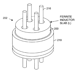
[0178] As shown in the drawings for purposes of illustration, the
present invention relates to a lossy ferrite inductor with both resistive and
inductive properties 200 (hereinafter referred to as "lossy ferrite
inductor"),
which is installed in proximity or adjacent to the hermetic terminal 202 of an
active implantable medical device (AIMD) 204. The lossy ferrite inductor 200
can be combined with a feedthrough filter capacitor assembly 206 which
includes a capacitor 208 having first and second sets of conductive electrode
plates 210, 212 embedded within an insulative or dielectric body 214, which is
mounted to the hermetic terminal 202 of the implantable medical device 204.
At least one feedthrough terminal pin or leadwire 216 extends through the
lossy ferrite inductor 200 in non-conductive relation. When used in
combination with a feedthrough capacitor 208, the feedthrough terminal pin
216 extends through the capacitor in conductive relation with the first set of
electrode plates 210. An an outer ferrule, housing or ground plane 218 is
mounted adjacent to the capacitor in conductive relation with the second set
of electrode plates 212.
[0179] The lossy ferrite inductor 200 works to absorb EMI energy
(convert to heat) and increase the impedance of the leadwire system 220 of
the implantable medical device 204. On the other hand, the feedthrough
capacitor 208, which is well known in the art, reduces the impedance to
ground thereby shunting or bypassing high frequency electromagnetic signals.
[0180] Feedthrough capacitors used by themselves are very effective
high frequency filters. However, due to capacitance, size, and circuit current
limitations, they are not very effective low frequency filters. The lossy
ferrite
inductor concept as disclosed herein is extremely effective for a pulsed RF
field. The lossy ferrite inductor 200 produces substantial series inductance
and series resistance at these frequencies. Accordingly, this raises the
impedance of the leadwire system 220 itself. The resistive component of the
lossy ferrite inductor also converts EMI from magnetic resonance imaging
(MRI) into harmless heat. This results in substantially reduced current into
the
leadwire system 220.
GREATB-47387
UTILITY APP
FILED 3/31/05
CA 02516034 2005-08-16
-25-
[0181] RF currents induced into a pacemaker leadwire system 220 can
be problematic in three ways: (1 ) there can be direct heating effects which
cause the temperature to rise to excessive levels in the leadwire; (2) current
flowing through body tissue 222 which can cause localized heating and body
tissue damage; and (3) RF currents which enter into the input circuitry 224 of
the cardiac pacemaker and cause the device to malfunction or fail
electronically. The lossy ferrite inductor concept would have minimal to
limited effect at a 1 kHz frequency. The reason is that the inductive
reactance
at this frequency is extremely low. Accordingly, the impedance of the
leadwire system 220 would really not be substantially affected. There is some
effect from resistive loss in the lossy ferrite inductor 200, but it too is
minimal.
The lossy ferrite inductor 200 concept as disclosed herein, has its highest
efficacy for attenuating the pulse RF field component of magnetic resonance
imaging. When combined with a feedthrough capacitor 208, this can reduce
leadwire current and also provide a very high degree of protection to the
electronics or input circuitry 224 of the medical device 204.
[0182] The novel lossy ferrite inductor concepts described herein will
substantially raise both the inductance and resistivity at the MRI RF field
frequencies. By raising the impedance of the implanted leadwire system 220,
currents are reduced in the leadwires and also in the area of the pacemaker
distal TIP electrode 226. The lossy ferrite inductor concept as described
herein will further substantially reduce the susceptibility of both the active
implantable medical device 204 and its associated leadwire systems 220 to
the effects of MRI and other hospital diagnostic or surgical equipment.
[0183] The addition of the novel lossy ferrite inductor 200 increases the
number of poles of the filter element. L, Pi, T, LL, 5 element and even n
element circuits can all be realized. These circuits can have the lossy
ferrite
inductor 200 pointing toward the body fluid side of the system, towards the
implantable medical device side of the system, or both. Increasing the
number of poles, as previously described in U.S. Patent Application Serial No.
10/825,900, increases the attenuation slope of the EMI filter as shown in FIG.
21. Accordingly, the novel lossy inductive ferrite concepts described herein
not only raise the impedance of the leadwire system, but they also greatly
improve the attenuation and effectiveness of the EMI filter installed at the
GREATB-47387
UTILITY APP
FILED 3/31/05
CA 02516034 2005-08-16
-26-
input to the implantable medical device. As previously described in U.S.
Patent Application Serial No. 10/825,900, commonly used EMI filters are
single pole devices consisting of a feedthrough capacitor and sometimes
backed up by onboard rectangular MLCC chips. Adding multiple capacitor-
s inductor elements makes the feedthrough attenuation slope much steeper.
Accordingly, this reduces the frequency at which the EMI filter starts to
become effective (lowers its 3 dB point). Previous EMI filters offer effective
attenuation at frequencies of 450 MHz and above. The novel multi-element
EMI filtered feedthrough capacitor - inductor circuits described herein will
create EMI filter circuitry that starts to become effective at 1 MHz and
above.
This is a substantial decrease in the frequency at which the EMI filter starts
to
become effective in comparison with the prior art.
[0184] This is not only important for MRI, lithotripsy and other
diagnostic procedures. The patient environment is increasingly becoming
more complex. New and more powerful emitters have recently been
introduced to the marketplace, including cellular telephone amplifiers, high
gain antennas for cellular telephones, cellular telephone jamming equipment,
and both fixed and portable radio frequency identification (RFID) scanners
and readers. These RFID scanners produce a very powerful (4 watts) digitally
modulated field that is typically 13.56 or 915 MHz. Some systems work at
other frequencies . Improved EMI filters as described herein will provide a
much higher degree of immunity for the implantable medical device 204 from
these new powerful emitters.
[0185] Also described are methods for preventing the lossy ferrite
inductor 200 from saturating in the presence of extremely large DC, low
frequency AC, and higher frequency RF fields. The present invention
includes novel field cancellation effects due to the time difference of
induced
currents imposed in body fluid due to an incident electromagnetic field. The
inventor has analyzed models of the complex permittivity of body tissue from
various references. Wave propagation of high frequencies increases in body
tissue thereby shortening the wavelength. This means that a substantial
phase angle will occur between signals induced in the right ventricle leads as
opposed to, for example, a biventricular lead placed outside the left
ventricle.
An example of these calculations is provided as follows:
GREATB-47387
UTILITY APP
FILED 3/31/05
CA 02516034 2005-08-16
-27-
[0186] Complex permittivity:
s=sr _Jsr
Using the complex permittivity model for tissue from- S. Gabriel, R.W. Lau,
and C. Gabriel, The Dielectric Properties of Biological Tissues: III.
Parametric
Models for the Dielectric Spectrum of Tissues.
_ 4En
~ E~ +~ 1+(jC~Z")~~ an) + j~~,o
Using the numbers for the above parameters for heart tissue, the calculated
complex permittivity at 64MHz is:
s =106.52 - j190.55
Therefore:
er =106.52
e; =190.55
The total conductivity from the tissue is the sum of the static ionic
contribution,
n;, and the alternating field conductivity, given by [1 ]:
~a = ~~o Er
~ _ ~; + ~u = 0.7281 S/m
The phase constant is calculated from the real part of the dielectric constant
and the total conductivity by [1]:
2
2
,Q = ~ ,usos 1 1 + ~ + 1
~ 2 ~Eosr
~3 =17.4120 rad/meter
The wavelength and phase velocity are given by:
~. = 2~ = 0.454 meters
v= ~ = 3.676 x 10⁶ meters/sec
Assume that the separation in lead TIPs in an enlarged heart (congestive
heart failure) is about 10cm (~4in), and convert the phase constant from
radians/meter to degrees/meter:
,Q =17.4120 rad x 180 deg = 997.6 deg
m ~c rad meter
997.6 deg x 0.1 meters=99.76 degrees phase difference
meter
GREATB-47387
UTILITY APP
FILED 3/31/05
CA 02516034 2005-08-16
-28-
Therefore the calculated phase difference between two points separated by
10cm in heart tissue for an electromagnetic wave with a frequency of 64MHz
is approximately 99.76 degrees.
References
1. C.A. Balanis, Advanced Engineering Electromagnetics, Wiley, 1989.
2. S. Gabriel, R.W. Lau, and C. Gabriel, "The Dielectric Properties of
Biological Tissues: III. Parametric Models for the Dielectric Spectrum of
Tissues", Phys. Med. Biol., vol. 41, pp.2251-2269 (1996).
[0187] The equations show that between the right ventricle and the left
ventricle, an induced phase difference of 99.76 degrees can occur at a typical
64 MHz MRI pulsed RF field. This is a significant phase difference that can
be used to reduce the core saturation effects in common inductors. This will
be further described below. At other RF pulsed frequencies such as 128
MHz, the phase shifts will be even greater.
[0188] In many implantable medical devices 204, such as cardiac
pacemakers, there are only leads implanted into one cardiac chamber. For
example, single chamber bipolar pacemakers have one lead that drops into
the right ventricle. Normally, this lead system consists of a TIP 226 which is
embedded in myocardial tissue, and in a RING 228 which floats in the blood
pool of the right ventricle. Sensing and pacing pulses are applied between
TIP 226 and RING 228. Because of the close proximity of the TIP wire 230,
which is surrounded by a spiral shaped RING wire 232, in a single chamber
application there is little or no phase difference between the two leads as
they
are exposed to MRI signals. It is a novel feature of the present invention
however, to route the leadwires 230, 232 that pass through the novel lossy
ferrite inductor 200 in opposite directions. This produces field cancellation
effects preventing the lossy ferrite inductor 200 from saturating.
[0189] Another inventive concept described herein is the presence of
a cancellation antenna 234. This is a leadwire that exits the implantable
medical device 204 and is routed in a different direction within the body
tissue
or venous system 222. For example, in the case of a cardiac pacemaker,
leadwires are typically routed from either the left or the right pectoral
muscle
area into the subclavian vein and routed down through the vasculature into
the bottom of the right ventricle. During this procedure it would be
relatively
easy for the surgeon to also route an additional leadwire across the top of
the
GREATB-47387
UTILITY APP
FILED 3/31/05
CA 02516034 2005-08-16
_29_
subclavian vein in the opposite direction. This will allow for maximum
separation distance between the implanted leadwires thereby causing a
maximum phase shift at the input to the cardiac pacemaker. This would also
create additional field cancellation effects within the lossy ferrite inductor
200
as described herein.
[0190] The performance of any magnetic material will be degraded if
it is operated under large DC or low frequency AC biases (MRI produces both
of these effects). Under small bias conditions, increasing the applied
magnetomotive force H applied to a magnetic core device includes a
corresponding increase in magnetic flux B in the core. At some value of H,
the magnetic flux B stops increasing. Increasing H beyond this value results
in a rapid decrease in the permeability of the inductor. For this condition,
magnetic theory terms the device "core saturated," as it is unable to support
further increases in magnetic flux with increasing magnetomotive force input.
When the slope of the B-H curve becomes nearly flat, which means it is in
saturation, the instantaneous permeability (equal to the slope at the
operating
point) of the core will drop to a value of approximately one, or that of free
space. However, even under this condition, the lossy ferrite inductors 200
have desirable lossy characteristics at EMI frequencies. When at saturation,
the core will provide little noise attenuation. To attenuate MRI, it is
important
that the lossy ferrite inductor 200 maintain a large lossy impedance (ohmic
loss). Using the novel concepts described herein, lossy ferrite inductors 200
designed to have a high resistive component may be used effectively even in
the presence of a large low frequency magnetomotive force input.
[0191] In the description of the drawings which follows, functionally
equivalent components among the various embodiments will be designated
by the same reference number.
(0192] FIGURE 1 is an example of the various types of active
implantable medical devices 204 that currently in use. FIG. 1 is a wire formed
diagram of a generic human body showing a number of implanted medical
devices. 204A is a family of hearing devices which can include the group of
cochlear implants, piezeoelectric sound bridge transducers and the like. 204B
includes an entire variety of neurostimulators and brain stimulators.
Neurostimulators are used to stimulate the vegas nerve for example to treat
GREATB-47387
UTILITY APP
FILED 3/31/05
CA 02516034 2005-08-16
-30-
epilepsy, obesity and depression. Brain stimulators are similar to a
pacemaker-like device and include electrodes implanted deep into the brain
for sensing the onset of the seizure and also providing electrical stimulation
to
brain tissue to prevent the seizure from actually happening. 204C shows a
cardiac pacemaker which is well-known in the art. 204D includes the family
of left ventricular assist devices (LVAD's), and artificial hearts, including
the
recently introduced artificial heart known as the Abiocor. 204E includes an
entire family of drug pumps which can be used for dispensing of insulin,
chemotherapy drugs, pain medications and the like. 204F includes a variety
of bone growth stimulators for rapid healing of fractures. 2046 includes
urinary incontinence devices. 204H includes the family of pain relief spinal
cord stimulators and anti-tremor stimulators. Insulin pumps are evolving from
passive devices to ones that have sensors and closed loop systems. That is,
real time monitoring of blood sugar levels will occur. These devices tend to
be more sensitive to EMI than passive pumps that have no sense circuitry.
204 H also includes an entire family of other types of neurostimulators used
to
block pain. 2041 includes a family of implantable cardioverter defibrillators
(ICD) devices and also includes the family of congestive heart failure devices
(CHF). This is also known in the art as cardio resynchronization therapy
devices, otherwise known as CRT devices.
[0193] FIGURE 2 is an illustration of a unipolar leadwire system for a
cardiac pacemaker 204. Pacing pulses are delivered through the leadwire
system 220 to the right ventricle of the heart. In a unipolar system, the
leadwire TIP which is placed in the myocardial tissue 222 in the ventricle
produces a pulse. The return is to the titanium can of the cardiac pacemaker
204C which one can consider as ground. This completes the electrical circuit.
Unfortunately, this leadwire can also act as a very effective antenna, which
can pick up stray electromagnetic signals. The type of antenna configuration
illustrated in FIG. 2 is generally effective for electric fields. The pulsed
RF
field, which is generated by the body coil or head coil of an MRI, generally
has
both magnetic and electric field components.
[0194] FIGURE 3 illustrates a bounded loop area of the leadwire
system 220 shown in FIG. 2. This bounded loop area is how coupling from
magnetic fields can induce currents in the leadwire system 220. This comes
GREATB-47387
UTILITY APP
FILED 3/31/05
CA 02516034 2005-08-16
-31-
from Faraday's Law of Induction. As one can see from FIG. 3, the leadwire
system 220 does not form a complete loop. The bounded area is enclosed by
the conductive leadwire system on the left and is returned through body tissue
222' on the right. Body tissue, of course, is a high reluctance path which
thereby reduces the magnetic field coupling efficiency.
[0195] FIGURE 4 is a very complicated tracing of an actual patient X-
ray. This particular patient required both a cardiac pacemaker 204C and an
implantable cardioverter defibrillator 2041'. The corresponding leadwire
system 220, as one can see, makes for a very complicated antenna and loop
coupling situation. The reader is referred to the article entitled "Estimation
of
Effective Lead Loop Area for Implantable Pulse Generator and Implantable
Cardioverter Defibrillators" provided by the AAMI Pacemaker EMC Task
Force.
[0196] FIGURE 5 is a line drawing of an actual patient cardiac X-ray
of one of the newer bi-ventricular leadwire systems. The new bi-ventricular
systems are being used to treat congestive heart failure. This represents the
first time that it has been possible to implant leads outside of the left
ventricle.
This makes for a very efficient pacing system; however, the leadwire system
220 is quite complex. When a leadwire system 220, such as those described
in FIGS. 2, 3, 4 and 5 are exposed to a time varying electric or magnetic
field,
electric currents can be induced into the leadwire systems.
[0197] FIGURE 6 illustrates the leadwire system 220 of a single
chamber bipolar pacemaker 204C. In this case, the pacemaker housing or
can 236 is neutral. Two leadwires are routed in very close proximity to each
other down into the right ventricle as shown in FIG. 6. The TIP electrode 226
is implanted into myocardial tissue. Generally speaking, the RING electrode
228 floats in the ventricle blood pool and represents the return path. One can
think of the TIP 226 as being positive and the RING 228 as being negative for
a particular point in the pulse. When this leadwire system 220 is exposed to
an external electric or magnetic field, EMI signals can be induced into the
leadwire system. However, due to the close spacing of the two leadwires
230, 232, the induced EMI signals tend to be of the same phase and also the
same amplitude. In this situation, an MRl can induce high currents into the
leadwire system 220. As will be explained later, it would be desirable to
raise
GREATB-47387
UTILITY APP
FILED 3/31/05
CA 02516034 2005-08-16
-32-
the impedance of the leadwire system 220 and thereby minimize the induced
current.
[0198] FIGURE 7 illustrates a dual chamber leadwire system 220 and
220' using the same type of bipolar leadwires 230, 232 and 230', 232' as
described in FIG. 6. In this case, one of the leads is implanted into the
right
ventricle and the other lead is implanted into the right atrium. As previously
described for FIG. 6, the voltages induced into the right ventricle (RV) leads
would tend to be of similar amplitude and phase. When one now examines
the two leadwires (230', 232') that go to the right atrium, the same thing is
true. The EMI signal induced on each lead will tend to be of similar amplitude
and phase. However, when one compares the right ventricle EMI signal to
the right atrium EMI signal, there can be a substantial difference in phase
and
amplitude. This is because of the variable separation distance, d, as shown in
FIG. 7. As the incident electric or magnetic field passes through as a wave
front, there is a time difference due to the spacing or separation distance,
d.
This has the effect of inducing voltages and currents in the leadwire systems
220 and 220' that are no longer in phase. Referring once again to FIG. 7, one
can see that EMI waveform A is going through a maximum amplitude positive
portion of the sine wave while at the same time, the waveform B is going
through a correspondingly negative portion of its sine wave. This, of course,
represents an extreme and unlikely situation where the two EMI signals would
actually cancel each other at the input to the dual chamber pacemaker.
[0199] FIGURE 8 is a schematic diagram representing the input
impedance and coupling model for a single chamber pacemaker with a bipolar
leads. V;~ is the induced MRI or EMI noise voltage, which can be induced by
electric or magnetic field coupling into the pacemaker leadwire system. The
pacemaker lead system source impedance is shown as ZS. Z;n represents the
pacemaker circuit input impedance. C1 and C2 are prior art feedthrough
capacitor EMI filters.
[0200] FIGURE 9 is the schematic of a distributed element model for
a typical bipolar leadwire system for a cardiac pacemaker such as that shown
in FIG. 10. The distributed capacitance Cx, Cy and CZ (...C~) tend to be quite
low in value (just a few picofarads), accordingly, the pacemaker input
impedance (X~ of the feedthrough) becomes an important current conduction
GREATB-47387
UTILITY APP
FILED 3/31/05
CA 02516034 2005-08-16
-33-
path at MRI RF field frequencies. In FIG. 9, 236 is the titanium housing of
the
cardiac pacemaker 204C. The 0.5 ohms represents the capacitive reactance
of a typical EMI filter feedthrough capacitor at a 64 MHz MRI pulse field
frequency (ref. U.S. patent 5,333,095 and others). The heart, shown to the
right, presents an approximate 500 ohms impedance at RF frequencies. This
does vary from individual to individual, but 500 ohms is a good average value.
The inductance elements L1 and L2 shown in series with the TIP leadwire are
representative of the fact that this inductance is distributed along the
entire
length of the lead. In other words, this would be more accurate if this were
broken up into L1, L2, L3, L4 ..., LN. The same is true of the typically
coiled
RING connection wire consisting of L1' and L2'. A better representation would
be L1', L2', L3' ... LN'. In a like manner, R1 and R2 are really distributed
along
the entire length of the TIP lead 230 and as well; R1' and R2' are distributed
along the entire length of the RING lead 232. For the TIP wire, the total
resistance value is about 70 ohms. Referring now to the RING lead, the total
resistance is typically about 140 ohms. This is because the RING connection
wire 232 is typically coiled about the TIP wire 230 and is thereby longer.
Also
shown in parallel between the TIP and RING leadwires are CX, Cyand CZ
which represents the distributed capacitance along the length of the bipolar
leadwire. As before, a more accurate distribution is CX, Cy... C~. Also shown
are a number of voltage sources V1, V2, V3 and V4. These represent
distributed EMFs in the leadwire that arise when the MRI fields) couples with
the implanted leadwire system. There is a current that flows in this loop that
results from the EMFs and loop impedance. Raising the value of the
pacemaker input impedance from 0.5 ohms to a higher value would tend to
reduce the loop current. Accordingly, using novel techniques as described
herein, additional resistance and inductive reactance at the point of
pacemaker leadwire(s) ingress and egress is a desirable feature.
[0201] FIGURE 10 mechanically illustrates the bipolar leadwire
system 220 of FIG. 9 that connects an implanted cardiac pacemaker 204C to
cardiac tissue 222. The pacer is typically implanted into either the right or
the
left pectoral muscle area. The surgeon first constructs a tissue pocket. A
special guide wire is then inserted which pierces the subclavian vein. The
bipolar leadwire is then routed through the subclavian vein down through the
GREATB-47387
UTILITY APP
FILED 3/31/05
CA 02516034 2005-08-16
-34-
aortic arch conveniently into one of the chambers of the heart. Typically, a
conventional bipolar lead will be implanted in either the right ventricle, the
right atrium, or both. The bipolar leadwire has been designed to withstand
millions and millions of mechanical motions as the heart beats. Typically, the
bipolar leadwire consists of an inner coil 230 which connects to the TIP
electrode 226 at the distal end and an outer coil 232 which is wound around
the inner coil and connects to the RING electrode 228. The TIP 226 is
typically implanted directly into myocardial tissue, for example, the tissue
in
the bottom of the right ventricle. The RING 228 is placed at some distance
from the TIP 226 and is insulated from it. The RING 228 typically floats in
the
blood pool in the ventricle. Biological electrical signals are sensed between
TIP and RING. In addition, electrical pulses from the pacemaker 204 are
delivered by the bipolar leads and are imposed across the TIP 226 and RING
228 which stimulates myocardial tissue 222 (beat pulse). In the configuration
shown in FIG. 10, this would be typical of a pacemaker lead as opposed to an
implantable defibrillator lead. The system shown in FIG. 10 is typically
programmable wherein the lead can act as a unipolar system wherein the
RING becomes inactive and the pacing and/or sensing are between TIP 226
and the pacemaker metal housing 236.
[0202] Referring to FIGURE 10, one can see the outer coil 232 and
the inner coil 230. As one develops electrical models of the leadwire system
220 it should be noted that because of its larger diameter, the outer coil
232, if
it were stretched out in a straight line, would be longer than the inner coil
230.
This means that typically the resistance and inductance due to the leadwire of
the outer coil 232 will be higher of that of the inner coil 230. The
distributed
capacitances that forms between the outer coil 232 and the inner coil 230 is
through a dielectric insulation which keeps the inner coil and the outer coil
in
electrical isolation
[0203] Referring now to FIGURE 11, one can see a family of curves
from a researcher named Dr. Tobias Bossert in Germany. Dr. Bossert studied
the absolute impedance of various implanted unipolar leads in 1987. At low
frequency the leadwire impedance tends to be about 200 ohms and then
drops into the area of around 80 ohms (on average) above 20 MHz.
GREATB-47387
UTILITY APP
FILED 3/31/05
CA 02516034 2005-08-16
-35-
[0204] FIGURE 12 is the work from a researcher named Landsterfer
in 1999. Dr. Landsterfer did this work at the University of Stuttgart in
Germany. Dr. Landsterfer's work indicates that at low frequency the
implanted leadwire impedance can vary significantly. At high frequency
(above 200 MHz), the leadwire system tends to stabilize around 80 ohms.
[0205] FIGURE 13 is from work done by Hansen et al. in 1996.
These researchers indicate that implanted leadwire systems vary from 80
ohms to about 120 ohms at low frequency and then start to increase in
impedance at very high frequency. Referring now back to FIG. 8, as one can
see from this simplified model, the current that would be induced in the loop
due to exposure to a medical diagnostic procedure, such as MRI, would be
the input voltage V;~ divided by the sum of the leadwire impedance ZS, and the
input impedance of the cardiac pacemaker Z;~. If V;" is excessively high
and/or the sum of Zs + Z;n is too low, then excessive loop current I can lead
to
excessive heating and tissue damage to the patient. Additionally, excessive
loop current at high frequency can interfere with the proper operation of the
cardiac pacemaker or implantable defibrillator due to electromagnetic
interference effects. Accordingly, raising the pacemaker input impedance at
selective frequencies is highly desirable, as that will tend to reduce the
loop
current and all of the aforementioned effects. One of the problems with
raising the leadwire impedance is that it is highly undesirable to raise
leadwire
impedance at the biologic sensing frequencies or biological pacing
frequencies. At these frequencies, pacemaker input impedance is kept
relatively high. In general, cardiac biologic signals fall between the ranges
of
20 to around 1000 Hertz. The most important part of this frequency range is
from 20 to about 400 Hertz. If one were to significantly raise the impedance
of the cardiac pacemaker leadwire system at these frequencies, this would
make the pacemaker very inefficient. Pacing pulses would be degraded. In
addition, sensing of biological signals would be attenuated. Accordingly, what
is needed is a frequency selective device that will raise the input impedance
of the cardiac pacemaker leadwire system or other active implantable medical
device at selective frequencies while allowing biological frequencies to
freely
pass.
GREATB-47387
UTILITY APP
FILED 3!31105
CA 02516034 2005-08-16
-36-
[0206] A way to accomplish this is with a ferrite bead 238 as shown
in FIGURE 14. The suppression performance of ferrite beads can be traced
to their frequency dependent complex impedance. At lower frequencies, the
impedance of the bead is primarily dominated by its inductive properties. At
high frequencies, ferrite materials are dominated by their loss or resistive
properties. A major disadvantage however, of the ferrite bead 238 as shown
in FIG. 14, however, is twofold. That is, it has a relatively small diameter
as
shown in view 14A. When exposed to large time varying fields, such as those
as produced in magnetic MRI, the bead material can saturate. When there is
a magnetizing force H applied to ferrite materials, magnetic domains are lined
up. Secondly, due to its small size and inefficient form factor, there is
simply
not enough material in the ferrite bead 238 to keep lining up magnetic
domains indefinitely.
[0207] FIGURE 15 illustrates the ferrite core saturation curve for the
ferrite bead 238 of FIG. 14. As one increases the applied magnetizing force H
to above the operating region, one reaches an area called core saturation.
This is where the magnetic flux density B no longer increases. At this point,
the ferrite material is doing no more good than the permeability of free space
which is one. The performance of any magnetic material would be degraded
if it is operated under a large DC or low frequency AC bias. Under small bias
conditions, increasing the applied magnetomotive force H applied to a
magnetic core device induces a corresponding increase in magnetic flux B in
the core. However, at some value of H, the magnetic flux B stops increasing.
Increasing H beyond this value results in a rapid decrease in the permeability
of the device. For this condition, magnetic theory terms the device's core to
be saturated, as it is unable to support further increases in magnetic flux
with
increasing magnetomotive force input.
[0208] This is a major problem with the extremely large fields induced
during MRI procedures. A ferrite bead 238 of the type shown in FIG. 14
would saturate and become ineffective. Accordingly, the ferrite bead 238
would fail to do its job of raising the input impedance of the implantable
medical device. For these reasons, the ferrite bead 238 of FIG. 14 is not a
preferred embodiment of the present invention. As will be described, novel
GREATB-47387
UTILITY APP
FILED 3/31/05
CA 02516034 2005-08-16
-37-
lossy ferrite slabs with a diameter to height ratio greater than 1.0 are the
novel
and preferred embodiment.
[0209] FIGURE 16 illustrates a novel bipolar lossy ferrite inductor
200 of the present invention. This is shown bipolar for illustrative reasons
only. One skilled in the art will realize this could be quadpolar, hexpolar,
octapolar or any other number of leadwires 230, 232. The important point is
that by placing these leadwires 230, 232 that run to and from body tissue
through a common lossy ferrite inductor 200, one can obtain field
cancellation.
One can see that the EMI waveform that is induced in leadwire 230 reaches a
relative minimum at 90 electrical degrees. Referring now to leadwire 232, one
can see that the EMI waveform goes through a relative maximum at 90
electrical degrees. These waveforms produce corresponding magnetizing
forces Ba and Bb in the lossy ferrite inductor 200 as shown. However, these
two applied magnetizing forces are induced in opposite directions thereby
providing some degree of cancellation. If the waveforms as illustrated in FIG.
16 are of equal amplitude and out of phase as illustrated, complete
cancellation will occur which would be highly desirable. However, in an actual
application, this is unlikely to be the case. When one considers the
complicated leadwire systems 220 of FIGS. 4 and 5, one can see that
substantial cancellation will occur in the lossy ferrite inductor 200. This is
a
key feature of the present invention. Not only does the use of the lossy
ferrite
inductor 200 raise the input impedance of the implantable medical device due
to the sheer bulk and increased path length of the ferrite material, but field
cancellation can also occur when there are multiple leadwires. In summary,
the lossy ferrite inductor 200 of FIG. 16 has four primary advantages over the
discrete ferrite bead previously described in FIG. 14. The inductor 200 has a
more efficient form factor, more magnetic material, a longer mean magnetic
path length, and allows for magnetic flux cancellation so that it can operate
in
high field such as MRI.
[0210] FIGURE 17 illustrates a novel toroidal lossy ferrite inductor
200 using a high permeability ferrite core. Other cores could be used,
however, a high permeability lossy core is desired for an MRI application
where the currents are very high and high frequency resistive/lossy
dissipative
elements are desired. The coil assembly 292 shown in FIG. 16 has two
GREATB-47387
UTILITY APP
FILED 3/31/05
CA 02516034 2005-08-16
-38-
different leadwires a and b (230, 232), commensurate with those shown in the
bipolar leadwire system in FIG. 9. In a medical implant application, FIG. 17
is
novel in that as the leadwires 230, 232 come through the coil 200 they are
wound in opposite directions. Assuming that the induced currents is and ib
shown in the leadwires a and b are in phase and are in the same vector
direction, the opposite turn directions will cause 180 electrical degree out
of
phase flux density Ba and Bb in the core C.
[0211] Referring now to FIGURE 18, one can see the novel lossy
ferrite coil assembly 292 of FIG. 17 shown installed in conjunction with the
typical EMI filter capacitor of a cardiac pacemaker 204C. EMI filter
capacitors
208 for cardiac pacemakers are well known in the art and are described by a
number of existing patents, including U.S. 5,333,095. Referring once again to
FIG. 17 the B-H loop cancellation lossy ferrite coil assembly 292 can be co-
bonded to the EMI filter capacitor 208 as shown.
[0212] FIGURE 19 is an outline drawing of the front view of a human
torso showing a cardiac pacemaker 204C that has been implanted in the right
pectoral muscle area. As is common in the art, a bipolar pacemaker leadwire
system 220 has been threaded through the subclavian vein and down into the
cardiac right ventricle. Shown is a novel phase cancellation antenna wire 234.
This is an additional wire that egresses through the EMI filtered hermetic
terminal 202 and the lossy ferrite inductor 200 of the cardiac pacemaker. This
insulated unipolar leadwire 234 does not have a TIP or RING electrode and is
not designed to connect to body tissue or fluid at all. It simply floats in
the
blood stream. The purpose of the phase cancellation antenna 234 is so that
when an MRI field, such as that produced at 64 MHz, induces currents on
both the right ventricle bipolar lead and the phase cancellation leadwires,
those currents will be subject to additional phase shift. This is because of
the
velocity of propagation of the MRI electromagnetic wave through myocardial
222 and other body tissue 222' and the fact that the cancellation leadwire 234
is spaced further apart from the bipolar leadwire 220 that provides pacing and
sensing to cardiac tissue. By having a wide and variable spacing between the
cardiac leadwires 220 and the phase cancellation lead (antenna) 234, MRI
currents that enter the pacemaker 204C will not be in phase. This is another
novel way to use phase cancellation to avoid core saturation in the lossy
GREATB-47387
UTILITY APP
FILED 3/31/05
CA 02516034 2005-08-16
-39-
ferrite inductor 200. This technique can be used as a stand alone feature or
in combination with the other phase cancellation methods described herein
(such as winding ferrite slab turns in opposite directions). It will be
obvious to
those skilled in the art that the phase cancellation antenna lead 234 can be
placed in a variety of directions and locations in the venous system or even
in
body tissue 222. It will also be obvious that phase cancellation leads) can
also be used in combination with atrium, left ventricle, cochlear,
neurostimulator and a wide variety of other implanted leadwire systems.
[0213] FIGURE 20 shows common EMI filter circuits such as C, L, PI,
etc. It is only the C circuit that has been in common use in cardiac
pacemakers to date (U.S. 5,333,095 et. al.). The L~, L2, Pi, T, LL and 5
Element circuits are desirable low pass circuit configurations for use with
either the novel lossy ferrite inductor or cancellation winding technology
described herein.
[0214] FIGURE 21 illustrates attenuation slope curves for various low
pass filter circuits as previously described in U.S. Patent Application Serial
No. 10/825,900. Shown are the attenuation slopes for C, L, Pi, T, LL and 5
element EMI filters. As one increases the number of filter elements, the
attenuation slope increases. That is, for a given capacitance value, one can
achieve a much higher level of EMI attenuation. For MRI applications,
particularly desirable configurations include the T or LL. The reason for this
is
that the added inductance and high frequency resistance also raises the
cardiac lead system impedance. As illustrated in FIG. 9, increasing the lead
system impedance reduces the MRI currents that circulate in the implanted
leadwires. This will substantially reduce undesirable leadwire heating
effects.
(0215] FIGURE 22 is a cross-sectional view of a quadpolar
hermetically sealed terminal 202 with a co-bonded quadpolar feedthrough
capacitor 208 and a quadpolar lossy ferrite inductor 200 of the present
invention. Feedthrough capacitors 208 are well known in the art. However,
feedthrough capacitors generally do not do much to improve the EMI
immunity of cardiac pacemakers and implantable defibrillators to high power
level hospital procedures, such as MRI. In fact, a large value feedthrough
capacitor can actually act to make the MRI situation worse. Feedthrough
capacitors work by making the input impedance of the cardiac pacemaker
GREATB-47387
UTILITY APP
FILED 3/31/05
CA 02516034 2005-08-16
-40-
very low at EMI frequencies. However, as previously described, a low input
impedance at MRI frequencies is exactly the wrong thing to have. The reason
is that this would cause increased loop currents in the cardiac leadwires. A
feedthrough capacitor of large value when exposed to MRI frequencies would
look like a very low input impedance and tend to short out the input of the
cardiac pacemaker or other active implantable medical device. This would
indeed protect the internal electronics of the cardiac pacemaker, but it would
also result in large loop currents in an implanted leadwire system. It has
been
shown in the literature that high loop currents can cause excessive heating
either in the leadwires or at the TIP to RING electrode interface which can
lead to patient tissue damage. These effects are described by Roger
Christoph Luchinger, reference attachment DISS.ETH14665. Doctor
Luchinger points out that if a cardiac pacemaker wearer is exposed to MRI, in
certain cases the pacemaker capture level can increase after the MRI
procedure. What this means is that the pacemaker may have to produce a
much higher voltage in order to properly pace the myocardial tissue. Post
mortem analysis has indicated that this increase in capture level was caused
by tissue damage at the TIP to RING interface of the cardiac leadwire system.
[0216] Referring once again to FIGURE 22, as one can see, it is the
lossy ferrite inductor 200 that is the primary component of importance when
attempting to raise the input impedance of the cardiac pacemaker at selected
frequencies (such as 64 MHz).
[0217] FIGURE 23 is a perspective view of the quadpolar lossy ferrite
inductor 200 and capacitor 208 of FIG. 22.
[0218] FIGURE 24 is a cross-sectional view of a unipolar hermetic
terminal 202 with attached feedthrough capacitor assembly 206 including a
lossy ferrite inductor 200.
[0219] FIGURE 25 is the schematic diagram of the LC EMI filter of
FIG. 24. The resistive element RL represents the lossy element of the lossy
ferrite inductor which converts unwanted RF energy to harmless heat.
[0220] FIGURE 26 is an isometric view of the lossy ferrite inductor
200 of FIG. 24.
[0221] FIGURE 27 illustrates the LC filter of FIG. 24 with a second
lossy ferrite inductor 200' added to the primary lossy ferrite inductor 200.
This
GREATB-47387
UTILITY APP
FILED 3/31/05
CA 02516034 2005-08-16
-41-
illustrates the advantage of having a very thick lossy ferrite inductor 200
which
increases the overall magnetic material and reduces its tendency to saturate
in the presence of high applied magnetizing force H. As previously described
in U.S. Patent Application Serial No. 10/825,900, it is not necessary that
ferrite material 200 be the same as ferrite material 200'. By using two
different material compositions, one could optimize the impedance at MRI
frequencies.
[0222] FIGURE 28 is an electrical schematic diagram of the filter
shown in FIG. 27.
[0223] FIGURE 29 is a view showing the co-bonding of two lossy
ferrite inductors L (200) and L' (200') utilizing a bonding washer 242. It
will be
obvious to one skilled in the art that these lossy ferrite inductors could be
stacked up in 3, 4 or more layers.
[0224] FIGURE 30 illustrates an embedded feedthrough capacitor C
with a lossy ferrite inductor L (200) shown co-bonded to it.
[0225] FIGURE 31 is the electrical schematic diagram of FIG. 30.
[0226] FIGURE 32 is an exploded view showing an internally
grounded capacitor C with five feedthrough wires 216 designed to go to
cardiac tissue. Internally grounded feedthrough capacitors are well know in
the art as described by U.S. Patent Nos. 5,905,627and 6,529,103. The lossy
ferrite inductor L (200) is shown in position to be co-bonded to the
feedthrough capacitor C. As previously described, the various signals
induced on these five leadwires would tend to produce magnetic flux density
(B) cancellation inside of the lossy ferrite inductor. This would allow the
lossy
ferrite inductor to continue to operate in the presence of very large fields,
thereby effectively increasing the input impedance of the implantable medical
device.
[0227] FIGURE 33 illustrates a lossy ferrite inductor L2 (200') placed
on the body fluid side of the hermetic terminal 202. In addition, there is a
second ferrite slab L1 (200) placed on the opposite side of the feedthrough
capacitor C (208) towards the internal electronics. This makes for what is
known in the art as a T-section filter.
[0228] FIGURE 34 is an isometric view of the lossy ferrite inductors
200, 200'.
GREATB-47387
UTILITY APP
FILED 3/31/05
CA 02516034 2005-08-16
-42-
[0229] FIGURE 35 is the schematic diagram of the T filter shown in
FIG. 33.
(0230] FIGURE 36 illustrates a novel double L (LL) circuit
configuration. In this case, the first capacitor 208 is oriented toward the
body
fluid side. There are two lossy ferrite inductors 200, 200' sandwiched
between the two capacitors 208, 208' as shown. Inductor 200' is towards the
pacemaker electronic circuits. The lower capacitor C1 is a hybrid capacitor in
that it has both an external and internal ground. The internal ground
communicates through a conductive via hole. This via hole can contain a
ground pin or be filled with a conductive material such as a thermal setting
conductive adhesive, a solder or the like. The important thing is that the
ground hole of the novel hybrid capacitor C1 communicates with the ground
plates of the upper capacitor C2. It is in this way that the ground electrodes
of
capacitor C2 are connected to a RNF ground point. In the case where the via
hole is filled with a conductive medium CM, it is preferable to have
additional
insulation on the inside diameter of the inductor slab L1 as shown. This is
shown as material b and can be of the group of any insulating material
including non-conductive polymers, non-conductive epoxies, insulating
sleeves, insulating tubing and the like. The upper and lower feedthrough
capacitors both have internal metallization a and a' in order to conduct their
respect ground electrode plates in parallel. The conductive fill medium that
connects the two capacitors together makes contact to this metallization a and
a'. The outside diameter metallization of the lower feedthrough capacitor C1
is
connected with material M which in a preferred embodiment is a thermally
conductive thermal setting material. M makes contact to the gold braze area
d to provide a reliable oxide free electrical connection to the ferrule 218.
The
ferrule 218 is connected to the overall housing which is the electromagnetic
shield of the implantable medical device (not shown). In this way the ground
electrode plates of both the lower and upper capacitors C1 and C2 become a
part of the continuous overall electromagnetic shield of the active
implantable
medical device. Referring once again to the via hole fill material CM, this
could also be a solid pin such as a copper pin or a nickel pin wherein this
would be soldered or installed by using a thermal setting conductive adhesive
to make contact with the capacitor respective ground electrode plate
GREATB-47387
UTILITY APP
FILED 3/31/05
CA 02516034 2005-08-16
-43-
termination a and a'. The LL configuration is particularly effective in that
it has
a very high attenuation slope rate (see FIG. 21 ). However, it would be
preferred in an MRI application to have the inductance point towards the body
fluid side. The reason for this is that capacitor 208 tends to lower the input
impedance of the cardiac pacemaker. This causes a corresponding increase
in MRI currents in the cardiac leadwires. Accordingly, it would be preferable
to have lossy ferrite inductor 200 swapped in place of capacitor 208 so that
higher input impedance could be presented to the implanted leadwire system.
Accordingly, FIG. 36 does not represent the best preferred embodiment.
[0231] FIGURE 37 is a schematic diagram of the LL EMI filter
assembly 206 shown in Figure 36. FIG. 38 is one possible top view of the LL
section quadpolar feedthrough capacitor described in FIG. 36. It will obvious
to those skilled in the art that other configurations (square, rectangular,
etc.)
and lesser or more leadwires are possible.
[0232] FIGURE 39 illustrates another form of the LL capacitor
previously described in FIG. 36. The previously described LL capacitor in
FIG. 36 has a combination of a hybrid capacitor incorporating both an external
and internal ground 208 and a conventional internally grounded capacitor
208'.
[0233] Referring to the LL filter of FIG. 39, one will see the capacitors
208 and 208' are conventional feedthrough capacitors with an external
metallized ground connection. The capacitor ground connections are made
by the conductive thermal setting material 246 as shown. In the preferred
embodiment 246 would be a silver filled conductive polyimide or the
equivalent. As one can see the silver fill makes contact to gold braze 248 and
is run up across the insulated ferrite slab 200 so that it also makes contact
with the outside diameter metallization of feedthrough capacitor 208'. It will
be
obvious to those skilled in the art that other materials could be used for the
conductive material 246 including solder, brazes, conductive epoxies and the
like.
[0234] FIGURE 40 is a sectional view through the capacitor 208'
illustrating the configuration of the ground electrode plates.
GREATB-47387
UTILITY APP
FILED 3/31/05
CA 02516034 2005-08-16
-44-
[0235] FIGURE 41 is a sectional view taken generally along the line
41-41 of FIG. 39, illustrating the configuration of the active electrode
plates
within the capacitor 208'.
[0236] FIG. 42 illustrates yet another embodiment of a LL capacitor
previously described in FIG. 36. In this case, the ferrule 218 of the hermetic
terminal has been extended upward so as to provide an annular space that
surrounds the feedthrough capacitors 208 and 208'. The conductive material
246 as previously described in FIG. 39 is placed to make an electrical contact
to both of the capacitor outside diameter ground termination areas.
[0237] FIGURES 43, 44, 45 and 46 describe the hybrid feedthrough
capacitor 208 previously described in FIG. 36. FIG. 43 is an isometric
drawing of feedthrough capacitor 208. FIG. 44 is the cross-section of said
capacitor 208. FIG. 45 represents the active electrode plates and FIG. 46
represents the ground electrode plates.
[0238] FIGURE 47 is an isometric drawing of the sintered lossy ferrite
inductors 200 and 200' that are shown in cross-section FIG. 36. FIG. 48
illustrates that said slab inductors have been conformally coated with
insulative material 244. In a preferred embodiment, material 244 would be
Paralene D. Paralene D is a vapor deposited high temperature tempered
conformal coating material. It can withstand high temperature laser welding
operations typical in cardiac pacemaker assembly. It can also withstand high
voltage as is typical in ICD applications. Paralene D also has excellent wear
and scratch resistance properties which makes it easy to handle during
manufacturing.
[0239] FIGURE 49 is an isometric drawing of the upper feedthrough
capacitor 208' of the LI_ filter previously described in FIG. 36.
[0240] FIGURE 50 is the cross-section of the upper quadpolar
capacitor 208' of FIG. 49. This is an internally grounded feedthrough
capacitor previously described in US Patent 5,905,627. FIGS. 51 and 52
illustrate the active and ground electrode plates 210, 212 of the internally
grounded feedthrough capacitor shown in FIG. 49.
[0241] FIGURE 53 illustrates the preferred embodiment of a LL EMI
filter in that the lossy ferrite inductor 200 is now oriented toward the body
fluid
side. As one can see, the previously described hybrid capacitor 208 is
GREATB-47387
UTILITY APP
FILED 3/31/05
CA 02516034 2005-08-16
-45-
attached to an elevated ferrule 218 flange with conductive bonding material
246. An additional gold sputter or braze or equivalent material 248 has been
added to the top of the ferrule flange 218 so that a reliable oxide free
electrical
connection can be formed from the outside diameter metallization 250
(ground metallization) of feedthrough capacitor 208 to the ferrule 218 (see
U.S. patents 6,765,779 and 6,765,780).
[0242] FIGURE 54 is the schematic diagram of the LL EMI filter
described in FIG. 53. As one can see, it is desirable to have lossy ferrite
inductor L~ (200) oriented towards the body fluid side. This has the effect of
raising the implanted leadwire impedance and electrically isolating the
feedthrough capacitors 208 and 208'. Also oriented toward the body fluid side
is resistor RL~. This is the high frequency lossy or ohmic electric
characteristic
of the novel lossy ferrite inductor 200. By orienting L~ and RL~ both towards
the body fluid side, this serves to raise the impedance of the leadwire
system.
As previously mentioned, this is highly desirable to reduce the amount of MRI
current flowing in the leadwire system. Less current means less heating and
less tendency to cause venous or TIP/RING ablation (tissue damage). Such
overheating has been noted in the reference literature and is highly
undesirable.
[0243] FIG. 55 is very similar to FIG. 53 except that an additional
inductive element 200" has been added. This makes the feedthrough filter
assembly into what is known as a five element filter.
[0244] FIG. 56 is the schematic diagram of the five element filter. As
illustrated in FIG. 21, the five element filter has a very high attenuation
slope
rate. As one increases the number of pulls n of the low pass filter network
attenuation slope continues to increase. That is, 6, 7, 8 or even more
elements would be desirable. Each time one leaves the lossy conductor slab
with a corresponding capacitor, one adds additional pulls to the low pass
filter
circuit. However, due to the space limitations of an implantable medical
device, it is not likely that five element filters will be used. In actual
practice,
the preferred embodiment is practically limited to a LL which is also known as
a four element low pass filter.
[0245] FIGURE 57 illustrates a quad polar lossy ferrite inductor 200
shown co-bonded to a quadpolar feedthrough capacitor 208. This is better
GREATB-47387
UTILITY APP
FILED 3/31/05
CA 02516034 2005-08-16
-46-
shown in the cross-sectional view of FIG. 58. One can see that there is a leak
detection vent 252 in accordance with U.S. Patent No. 6,566,978 shown
through the device into passage or air space. This facilitates ready passage
of helium gas during a hermetic seal test.
[0246] FIGURE 59 illustrates an inline quadpolar lossy ferrite inductor
200 with multiple turns of insulated leadwire 216. This is shown co-bonded to
a inline quadpolar feedthrough capacitor 208. Adding multiple turns is very
efficient since the inductance increases as the square of the turns.
Accordingly, the lossy ferrite inductor 200 will have 4 times the inductance
as
if only one turn passed through it as shown in previous drawings. In
accordance with the present invention, the lossy ferrite inductor 200 raises
the
input impedance of the device and also which helps to protect it from MRI. In
addition, since the four leadwires 216 are placed in different areas of the
heart, substantial magnetic flux density cancellation can occur. This helps to
avoid saturation of the lossy ferrite inductor allowing it to properly operate
in
the presence of high fields.
[0247] FIGURE 60 is the schematic diagram of the LC filter of FIG.
59.
[0248] FIGURE 61 illustrates an improved inline lossy ferrite inductor
200 which facilitates passing multiple turns. This was previously described in
pending U.S. Patent Application Serial No. 10/825,900.
[0249] FIGURE 62 illustrates a dual inline hermetic terminal 202 with
bonded feedthrough capacitor C (208). There are eight active pins 216 and
one ground pin as illustrated. Accordingly, feedthrough capacitor C (208) is
an internally grounded capacitor with its ground electrode plates connected to
the grounded pin. Lossy ferrite inductor L (200) is shown ready for co-
bonding to the ceramic capacitor C (208). By placing all of the leadwires 216
through the common lossy ferrite inductor L (200) substantial magnetic flux
density cancellation due to out of phase signals is achieved. A novel alumina
substrate 254 with wire bond pads 256 is also shown ready for co-bonding.
This is also previously described in pending U.S. Patent Application Serial
No.
10/825,900.
[0250] FIGURE 63 illustrates yet another improved embodiment
wherein the lossy ferrite inductor L (200) is positioned toward the body fluid
GREATB-47387
UTILITY APP
FILED 3/31/05
CA 02516034 2005-08-16
-47-
side of the device. Accordingly, the feedthrough capacitor C (208) is pointed
towards the implantable electronics of the implantable medical device. This is
a quadpolar L-section filter device as illustrated in the schematic diagram of
FIG. 64. The top view could be rectangular, square or round as previously
shown. This is a highly desirable or preferred embodiment in that the lossy
ferrite inductor 200 acts to increase the impedance of the leadwire system.
By positioning capacitor 208 on the other side of the lossy ferrite inductor
200,
its relatively low impedance is then positioned to protect the internal
electronics, but not unduly lower the impedance of the leadwire system itself.
[0251] Referring now back to FIGURE 63, one can see that there is a
conductive polyimide material 246 which is attached to a gold braze area 248
of the titanium ferrule 218 of the hermetic terminal 202.
[0252] FIGURE 65 is very similar to FIG. 63 except that the
attachment material 246 is shown connected between the outside diameter of
the capacitor 208 and the inside diameter of the ferrule 218. Attachment
material 248 desirably contacts gold braze material 248 in accordance with
U.S. Patent No. 6,765,779.
[0253] FIGURE 66 is also very similar except that the conductive
polyimide material 246 is shown connected to a gold braze 248 which goes
across the entire top of a flange portion of the ferrule 218.
[0254] FIG. 67 is very similar to FIG. 63 except that the electrical
connection material 246 makes contact from the gold braze area 248 of the
hermetic terminal flange 218 across in a non-conductive relationship with the
inductor 200 to the outside diameter metallization of the feedthrough
capacitor
208.
[0255] FIGURE 68 is a cross-sectional view of an internally grounded
capacitor 208 of the present invention showing the lossy ferrite inductor 200
oriented towards the body fluid side.
[0256] FIGURES 69, 70 and 71 illustrate various possible top views
that correspond with the internally grounded feedthrough capacitor 208 of
FIG. 68. Accordingly, schematic diagrams 72, 73 and 74 illustrate various
possible schematic diagrams that go with the internally grounded feedthrough
capacitor 208 and lossy ferrite inductor 200 of FIG. 60.
GREATB-47387
UTILITY APP
FILED 3/31/05
CA 02516034 2005-08-16
-48-
[0257] FIGURE 75 is a cross-sectional drawing illustrating a "T"
circuit filter configuration. A "T" circuit is also highly efficient in that
lossy
ferrite inductor L~ (200) is oriented toward the body fluid side. Lossy
ferrite
inductor L2 (200') points toward the electronics of the implantable medical
device thereby tending to stabilize the device's input impedance. As
previously shown in FIG. 21, the "T" is a very high performance EMI filter
that
will offer broad attenuation throughout the frequency range from 1 MHz to 100
MHz and above. As previously mentioned, EMI filters using only a
capacitance C, generally are only effective from 100 MHz to about 3 GHz.
The "T" section filter as shown in FIG. 75, has all the benefits of a
feedthrough
capacitor 208, but with the added benefits of inductances and high frequency
dissipative losses placed on both sides of the feedthrough capacitor. The
performance of the T filter is not quite as high as the performance of the LL
circuit filter, however, it is outstanding compared to all prior art "C"
circuit
devices.
(0258] FIGURE 76 is very similar to the EMI filter assembly described
in FIG. 75. One can see, however, that it is smaller in diameter. Referring
back to FIG. 75, the relatively wide spacing between the two leadwires 216
and 216' is required in a high voltage implantable defibrillator application.
This is because high voltage fields tend to arc across surfaces. In other
words, it is very unlikely that a high voltage field would arc across the open
air
space as illustrated as letter a in FIG. 75. Referring once again to FIG. 76,
one can see that a novel slot feature has been added to the novel lossy
ferrite
inductor 200' of the present invention. This greatly increases the surface
path
length between pins 216 and 216'. Starting from the right edge of pin 216,
one can see that for an electric arc to follow the surface it would have to
travel
first along surface a then down along surface b across surface c, then up
surface d, and across surface a to reach the point of opposite polarity on the
left edge of pin 216'. In electrical engineering, this is called a tortuous
path.
In other words, the creepage distance from pin to pin has been significantly
increased. This same feature can be added many of the ferrite slabs of the
present invention including a ferrite slab on the body fluid side. For
example,
FIG. 33 illustrates a ferrite slab 200' that is shown on the body fluid side.
This
happens to be a unipolar device, but it will be obvious to one skilled in the
art
GREATB-47387
UTILITY APP
FILED 3/31/05
CA 02516034 2005-08-16
-49-
that if it were a multipin device that slots could be added to increase the
creepage distance. This can be increasingly important to components
exposed to body fluid in that tissue migration or even metal deposition can
occur across such surfaces. The reason for this is that in a pacemaker there
are electrical pulses present on the leads. There are also precious metal
such as gold plating that could migrate or electroplate out in the presence of
an electrolyte and voltage potential. Accordingly, an increased creepage path
as illustrated in FIG. 76 is easily applicable to all body fluid embodiments
illustrated in this patent. This is better illustrated by referring to the
isometric
view shown in FIG. 77. FIG. 77 is an isometric view of the upper inductor
lossy slab 200' previously described in FIG. 76. This is a quad polar device
with a crisscross slot providing the required tortuous path..One can follow
surfaces a, b, c, d, and a which greatly increases the clearance between the
pin location holes x and y.
[0259] Referring once again back to FIG. 76, there is another way
that a surface flash or high voltage arc over can occur. Starting at the right
side of pin 216' and tracing across surfaces f, g and h, one can see that if
pin
216' was at a positive high voltage relative to the capacitor outside diameter
termination z, then a voltage potential could occur across these surfaces.
Referring to FIGURE 76, the ferrule 218, which is designed to be welded to
the titanium housing of a pacemaker or other implantable medical device, is at
ground potential in this example. Electrical connection material 206 connects
ferrule rule 218 to the capacitor outside diameter metallization 250.
Accordingly, the outside diameter metallization 250 is at the same potential
as
the ferrule 218. In a preferred embodiment, a crosscut structure as shown in
FIG. 77, would be preferred over a similar structure shown in FIG. 78. The
reason for this is that the distance g (or height) is greater in FIG. 77 as
compared with FIG. 78. This increases the voltage standoff or tortuous path
tracing along surfaces f, g and h. In other words, by making g taller one
increases the voltage standoff capability from either pin 216 or pin 216' to
ground. Of course, in programmable implantable defibrillators, it is possible
to
have the can active. In other words, the ferrule 218 could be positive in
reference to pin 216' which could then be negative and so on. However, in all
GREATB-47387
UTILITY APP
FILED 3/31/05
CA 02516034 2005-08-16
-50-
cases it is desirable to have as much stand off distance as possible from pin
to pin and from pin to ground.
[0260] Comparing the outside diameter of the quad polar EMI filter
shown in FIG. 75 to the outside diameter of the quad polar filter shown in
FIG.
76, by using the novel slot technology as described in FIGS. 77 and 78, one is
able to make the overall EMI filtered terminal smaller. It will be apparent to
those skilled in the art that this novel slot or raised barrier technology in
the
ferrite inductor slab also applies to a wide variety of geometric shapes,
including rectangles, dual inline filters and so on.
[0261] FIGURE 78 performs a similar function in that it is a lossy
ferrite inductor of the present invention. However, in this case the increased
stand off distance from pin to pin has been accomplished by the raised
protrusion areas as shown. It should be noted that for all of the ferrite
inductor slabs as described herein, the lossy ferrite inductor has been coated
with a suitable insulating material. In the preferred embodiment, this would
be
high temperature tempered Paralene D. Accordingly, the novel lossy ferrite
inductors as described herein have excellent insulative properties and
dielectric strength.
[0262] Referring back to FIG. 77, one can see the slope area d.
This angular feature facilitates the manufacturing process. In a preferred
embodiment, the novel lossy ferrite inductors as described herein are
manufactured by powder formulations which are dispensed into carbon
fixtures to create the desired shapes. They are then fired at very high
temperature (sintered) to form a hard monolithic structure. It is after that
that
tumbling and Paralene coating is performed. However, after sintering, one
must be able to remove the hard fired lossy ferrite inductor from the fixture.
The angular feature d shown in FIGS. 77 and 78, simplifies this fixture
release. This feature could be vertical, however, this would decrease
manufacturing yields and also slow manufacturing time, as it would be very
difficult to remove the fired ferrite lossy slab from the fixture. The
fixtures
used are typically of graphite or carbon and are somewhat fragile. By
providing the angled tool feature d as shown in FIGS. 77 and 78, one also
increases the lifetime and reduces the wear on the manufacturing fixtures.
GREATB-47387
UTILITY APP
FILED 3/31/05
CA 02516034 2005-08-16
-51-
[0263] FIGURE 79 illustrates alternative embodiments showing a
convoluted structure similar to the insulator that would hang from a telephone
pole. These convolutions greatly increase the creepage distance from pin to
pin. Various cross-sections are shown in FIG. 79A, FIG. 79B and FIG. 79C.
It will be obvious to one skilled in the art that any number of possible cross-
sections are possible in order to increase the creepage path between the
opposing pins, for example, between pins x and y of FIG. 79. The structure
shown in FIG. 79 does present a significant fixturing issue during the
sintering
or firing of the lossy ferrite inductor. In this case, a multistage fixture
would
need to be manufactured which would be quite expensive to accomplish. For
this reason, the structure shown in FIG. 79 is not a preferred option.
[0264] FIGURE 80 is the schematic diagram of the quad polar EMI
"T" filter shown in FIGS. 75 and 76. Referring once again to FIG. 80, the
inductive and lossy elements L2 and RL2 come from the novel sintered ferrite
slab shown in FIGURES 77, 78 or 79.
[0265] FIGURE 81 is an isometric view of an inline quadpolar EMI
filter 206 mounted to the terminal 218 of an implantable medical device.
Feedthrough capacitor 208 is shown bonded in accordance with well-known
prior art techniques to the hermetic terminal 202. Lossy ferrite inductor 200
has four (quadpolar) leadwires 216 that penetrate through it. The leadwires
216 that penetrate through the lossy ferrite inductor 200 that are labeled a
and
c, go straight through the lossy ferrite inductor 200 and perform very much
the
same as the lossy ferrite inductors as previously described herein. Leadwires
a and b would typically be from one bipolar pair, for example, the bipolar TIP
and RING leadwire system 220 implanted into the cardiac right ventricle.
Leadwires c and d are from a different bipolar pair. The leadwires as
illustrated at points b and d are designed to wrap around the lossy ferrite
inductor 200 in the opposite direction. As previously discussed in FIG. 16,
this produces cancellation vectors B within the lossy ferrite inductor 200
preventing it from saturating. This means that the permeability of the lossy
ferrite inductor 200 is maintained even in the presence of high MRI fields.
The leadwires b and d would typically be from a different bipolar lead, such
as
that implanted in the right atrium or outside the left ventricle. In a bipolar
lead,
such as the right ventricle lead pair, there is very little phase shift in the
GREATB-47387
UTILITY APP
FILED 3/31/05
CA 02516034 2005-08-16
-52-
currents induced in the closely spaced TIP and RING wires from MRI. This is
due to the wave velocity of propagation and the relatively close spacing of
the
TIP and RING leadwires. However, for a bipolar lead placed in the right
ventricle (a and b) and a bipolar lead implanted in another physical location
such as outside the left ventricle (c and d), there is enough spacing between
the two bipolar lead pairs to create a substantial phase shift. Accordingly,
the
configuration shown in FIG. 81 is designed to take advantage of said phase
shift and reduce ferrite slab saturation in the presence of MRI field
gradients.
This is in addition to the phase cancellation effect of wrapping the
individual
bipolar pairs in opposite directions through the ferrite slab (such as a and b
if
the right ventricle was connected to them). This gives the designer many
options to handle phase cancellation.
[0266] FIGURE 82 is the schematic diagram of the "L1" circuit
quadpolar EMI filter described in FIG. 81.
[0267] FIGURE 83 is view 83-83 taken from FIG. 81 which shows the
penetration of the leadwires a and c straight through the lossy ferrite
inductor
200. As can be seen, leadwires a and c pass straight through both the
feedthrough capacitor 208 and the lossy ferrite inductor 200.
[0268] FIGURE 84 is a cross-section from FIG. 81 taken from section
84-84. As one can see, the leads b and d are routed around lossy ferrite
inductor 200 in such a way that they go through the center of inductor 200 in
the opposite direction compared to leadwires a and c. This causes a phase
shift for the induced EMI signals thereby producing additional cancellation
vectors within the lossy ferrite inductor.
[0269] FIGURE 85 is a typical active implantable medical device 204.
This could typically be a unipolar cardiac pacemaker, a unipolar
neurostimulator or the like. The device shown in FIG. 85 is a unipolar device
in that, one leadwire 216 which can be of any length, extends from the
implantable medical device 204 either through the venous system or through
body tissue itself to a distal Tip location. The distal Tip 300 includes a
probe
302 which is inserted into body tissue. The distal Tip can have a number of
shapes which are common in the art. For example, in a neurostimulator, the
distal Tip 300 would be placed in or around (as a coil) nerve tissue, for
example, to block pain signals in the spinal cord. There is also a unipolar
GREATB-47387
UTILITY APP
FILED 3/31/05
CA 02516034 2005-08-16
-53-
hermetic feedthrough 202 consisting of an alumina or glass insulator 240
which is then gold brazed 246 to the overall housing of the AMID 204. There
is also a hermetic gold braze connection 246' made between the hermetic
insulator 240 and the leadwire 216. Hermetic pin assemblies are well known
in the art and can be combined with a ferrule as shown elsewhere herein..
However, as shown in FIG. 85, a ferrule is not always necessary. In addition,
the gold braze materials 246, 246', which are typically of gold, are also not
always required. That is, glass copression seals can also be used to preclude
the entrance of body fluids into the interior of the AIMD.
[0270] AIMDs typically employ a circuit board or substrate 304 as
shown. This circuit board can be connected to an internal battery and various
electronic devices in order to provide an output pulse to stimulate body
tissue
and/or sense biological signals. The output pulse can be directed to a
number of leadwires, however, in FIG. 85, the simplest form is a unipolar
device. In this case, the output pulse is stimulated to body tissue with
reference to the AIMD can or housing and the distal lead Tip 302. In other
words, the metal housing of the AIMD a forms one electrode and the other is
the unipolar distal Tip electrode 302. As shown in other drawings herein, this
is not always the case. In other words, it is not necessary that the AIMD
housing (can) be a return electrode. For example, in a bipolar device the
pulse could be solely between two or more implanted leadwires. In a cardiac
pacemaker, this would typically be done using a bipolar lead, for example, in
the right ventricle where there is both a distal TIP and a distal RING
electrode.
[0271] Referring still to FIGURE 85, one can see the novel lossy
ferrite inductor 200 of the present invention which is positioned so that both
the ground leadwire 306 and the active leadwire 216 pass through the ferrite
inductor 200 in non-conductive relation. This is important so that the phase
cancellation techniques as described in the present invention are utilized.
That is, when this AIMD system is exposed to a powerful source of EMI such
as that produced by MRI, signals will be induced both on the metallic AIMD
can housing and on the distal lead system consisting of 216, 300 and 302. As
these signals go through the ferrite inductor 200, they will produce a magneto-
motive force which will result in magnetization forces within the lossy
ferrite
inductor 200 which will tend to be of different phases and partially or
totally
GREATB-47387
UTILITY APP
FILED 3/31/05
CA 02516034 2005-08-16
-54-
cancel one another. As described herein, this will help to prevent core
saturation within the lossy ferrite inductor 200.
[0272] Referring once again to the circuit substrate 304, one can see
that there are wire bond pads 308 and 308' which are connected to the
leadwires 306 and 216. An attachment is made to the wire bond pad either by
ultrasonic wire bonding, thermal sonic wire bonding, soldering or the like.
Circuit traces 310 and 310' are then routed to the electronic circuit modules)
312 of the AIMD.
[0273] The novel ferrite inductor 200 is shown in an intermediate
location between the point of lead ingress into the implantable medical device
housing and circuit substrate 304. As has been previously described in the
present invention, one preferred embodiment would be to co-bond the novel
lossy ferrite inductor 200 to the hermetic terminal assembly 202 a using a
suitable co-bonding adhesive washer or polyimide washer. It would also be
acceptable to co-bond the novel lossy ferrite inductor 200 directly to the
circuit
board 304 itself. What is important, is that the leadwires 306 and 216 pass
through the novel ferrite inductor in non-conductive relation.
[0274] The novel ferrite inductor 200 provides two very important
functions in the AIMD system. That is, the lossy inductor 200 raises the
impedance of the leadwire system thereby reducing the levels of currents
induced during MRI and other exposure to high intensity electromagnetic
fields. Reduction of such currents reduces the amount of heating in the
leadwire 216 and also the amount of heating at the distal Tip 302. Such
heating can be damaging to body tissue, lead to tissue necrosis, or result in
a
higher pacing impedance for the AIMD thereby reducing its efficacy.
Increased distal TIP impedance due to overheating means that the AIMD
must stimulate at a higher output voltage. This is undesirable as this
increases battery drain and leads to shortening the life of said device. The
lossy ferrite inductor 200 also provides another very important function in
that
it acts as a one-pole low pass EMI filter thereby providing a degree of EMI
protection to the sensitive electronic circuits of the AIMD. As described
throughout the present invention, one can greatly improve the amount of EMI
filtering by adding additional filter elements, such as feedthrough
capacitors. .
GREATB-47387
UTILITY APP
FILED 3/31/05
CA 02516034 2005-08-16
-55-
[0275] Referring once again to FIG. 85, the AIMD housing is typically
of titanium, stainless steel or other metals that are biocompatible. However,
it
should be stated that the present invention is not limited to AIMDs that have
a
metallic housing. In fact, AIMDs can also have a ceramic housing or other
insulative housing wich protects the AIMD electronics from body fluid
intrusion. Where the AIMD housing is insulative, a separate electrode is
typically provided, for example, a platinum electrode located on the ceramic
housing itself. There are certain AIMDs that incorporate a ceramic tube with a
titanium end cap. The end cap forms the housing electrode. It will be obvious
to one skilled in the art that the present invention, involving phase
cancellation
through a lossy ferrite inductor, could also include a ceramic housing with a
separate co-attached electrode.
[0276] FIGURE 86 illustrates a unipolar lossy ferrite inductor 200
bonded to the hermetic terminal 202 of an implantable medical device. It is
notable that there is no feedthrough capacitor in this particular application.
Indeed, just the presence of a lossy ferrite inductor 200 by itself will
greatly
improve the immunity of the implantable medical device to high intensity EMI
fields such as those created by MRI. However, the lack of a feedthrough
capacitor would make the implantable medical device more sensitive to high
frequency EMIs, such as that produced by cell phones and other emitters.
Accordingly, FIG. 86 is not the preferred embodiment, but is a suitable
embodiment if MRI is the primary concern.
[0277] FIGURE 87 is a schematic diagram of the hermetic terminal
202 of FIG. 86.
[0278] FIGURE 88 is a close-up isometric view of the Iossy ferrite
inductor 200 illustrated in FIG. 86.
[0279] FIGURE 89 is very similar to FIG. 86 except that the lossy
ferrite inductor 200 is shown embedded within the flange 218 of the hermetic
terminal 202. An optional epoxy fill EP can be added for cosmetic purposes.
[0280] FIGURE 90 is the schematic diagram of FIG. 89.
[0281] FIGURE 91 is a five-leaded device showing a lossy ferrite
inductor 200 ready for co-bonding to the hermetic terminal 202. The hermetic
terminal 202 consists of a titanium ferrule 218 and alumina ceramic insulator
GREATB-47387
UTILITY APP
FILED 3/31/05
CA 02516034 2005-08-16
-56-
240. Hermetic sealing is achieved by co-brazing using a pure gold braze of
the elements.
[0282] FIGURE 92 shows a lossy ferrite inductor L (200) which is
embedded within the flange 218 of the implantable medical device. This is
better illustrated in the cross-sectional view shown in FIG. 93. One can see
that the lossy ferrite inductor L (200) is embedded and encapsulated in a
material so that it cannot move. Such material is a non-conductive epoxy
material which is simply used to mechanically hold the lossy ferrite inductor
200 in place. There is no electrical attachment required or desirable between
the lossy ferrite inductor and the flange 218. In fact, for all of the lossy
ferrite
inductors 200 as shown herein, the lossy ferrite inductor 200 has been treated
with a suitable conformal coating material 244, such as Paralene to improve
its dielectric breakdown strength or resistance to application of voltages.
[0283] Referring now back to FIGS. 92 and 93, one can see that the
lossy ferrite inductor L (200) has a novel leak detection vent hole 252 to
facilitate helium leak detection.
[0284] Referring now to FIGURE 94, one can see an inline quadpolar
lossy ferrite inductor 200 similar to that previously described in FIG. 59,
except that the feedthrough capacitor has been removed.
[0285] FIGURE 95 is the schematic diagram of the lossy ferrite
inductor L (200) of FIG. 94.
[0286] FIGURE 96 shows an improved lossy ferrite inductor 200
which could be co-bonded to the hermetic terminal 202 shown in FIG. 94.
The modified lossy ferrite inductor L (220) has been adapted to accommodate
additional turns. The slot features keep these turns separated so adjacent
turns will not short out. Using the lossy ferrite inductor 200 configuration
illustrated in FIG. 96, two, three or even more turns can be used.
[0287] FIGURE 97 is very similar to that previously described in FIG.
62, except that the internally grounded feedthrough capacitor C has been
removed.
[0288] FIGURE 98A through 98D illustrate various examples of the
shapes that the lossy ferrite inductor L (200) can take on. The lossy ferrite
inductor 200 is preferably made of pressed powders. These powders are
mixed with a binder system which is shape formed by pressing the powder
GREATB-47387
UTILITY APP
FILED 3/31/05
CA 02516034 2005-08-16
-57-
into a die. The die can take on any shape of which is limited only by one's
imagination. FIG. 98A illustrates a round lossy ferrite inductor. FIG. 98C is
rectilinear. FIG. 98B is oval or elliptical and FIG. 98D indicates that any
other
shape with cutouts, T shapes or even triangles are possible. After the
pressed pellet is formed, the lossy ferrite inductor is fired at high
temperature
sintering it into a hard monolithic structure.
[0289] FIGURE 99 illustrates the housing 236 of a cardiac pacemaker
204 with a hermetic terminal 202 which is typically laser welded into the
titanium housing 236. In this embodiment, however, the lossy ferrite inductor
200 is shown bonded onto a multilayer circuit board 224 (shown greatly
enlarged). Of course, the implantable medical device 204 would have many
other internal components, including a battery, reed switch, hybrid circuits,
etc. The purpose of FIG. 99 is to indicate that the lossy ferrite inductor 200
will perform to raise the inductance anywhere it is placed in the circuit.
(0290] FIGURE 100 illustrates that the lossy ferrite inductor 200 can
be placed intermediate between the hermetic terminal 202 and circuit boards
224 or other components within the implantable medical device and perform
to raise the impedance.
[0291] FIGURES 99 and 100 also show an optional feedthrough
capacitor 208 which is well known in the art as a high frequency EMI filter.
When the lossy ferrite inductor 200 is used in combination with the
feedthrough capacitor 208, this makes a very effective L section filter as
described in co-pending U.S. Patent Application Serial No. 10/825,900.
However, for the purpose of attenuation of MRI pulses, it would be desirable
to have the lossy ferrite inductor 200 as shown in FIGS. 99 and 100 towards
the body fluid side of the feedthrough capacitor 208. As previously described,
this is important to reduce loop currents. Also, this isolates the relatively
low
impedance of the feedthrough capacitor 208 from the implanted leadwire
system thereby reducing heating effects of MRI in the leadwire system.
[0292] FIGURES 101 and 103 illustrate a novel feature of the present
invention in that lossy ferrite inductors 200, 200' with a very small center
hole
can be manufactured and then layered to provide the overall height to
optimize both the inductive and resistive properties. In FIG. 101 one sees
that
there are two ferrite slabs 200 and 200' which have been bonded together
GREATB-47387
UTILITY APP
FILED 3/31/05
CA 02516034 2005-08-16
-58-
with a non-conductive insulating washer 242. This allows one to increase the
overall height of the lossy ferrite inductor without running into the
fixturing
problems if one tried to manufacture this as a single element. As previously
mentioned, for a single lossy ferrite inductor 200, the height and inside
diameter ratio could be quite problematic in the manufacturing operation.
[0293] It will be obvious to one skilled in the art that two, three or a
number of Iossy ferrite inductors 200 can be co-bonded together to achieve
any desired height and total inductance that is required.
[0294] The schematic diagram shown in FIG. 102 illustrates the effect
of having these two lossy ferrite inductors 200 and 200' acting in series with
their two resistive properties acting in series. These elements simply add up
which increases the overall inductance and the overall resistance of the lossy
ferrite inductor. However, this does not change the basic EMI low pass filter
circuit configuration. In other words, the addition of a second lossy ferrite
inductor 200' means that the EMI filter of FIG. 101 still acts as a single
element section filter. It is only when you separate the ferrite slabs by a
capacitor element that you increase the number of poles or elements of the
EMI filter, as described further herein.
[0295] Referring now back to FIG. 101, one can see that a plurality of
lossy ferrite inductors 200 and 200' can be co-bonded together. These slabs
can be of various initial permeabilities and properties. For example, the
first
slab 200 could be of manganese zinc material and slab 200' could be of
cobalt zinc material. These two materials have markedly different electrical
properties. One material has higher inductance at low frequency whereas the
other material has higher inductance at higher frequencies. By co-bonding
lossy ferrite inductors 200 and 200' of various materials together, one can
optimize inductance throughout wider frequency ranges. The same is true of
the resistive property RL1 and RL2 of the two lossy ferrite inductors 200 and
200'. Each type of ferrite material has different resistance versus frequency
properties. By combining various materials one can also optimize the amount
of resistance versus frequency.
[0296] Another novel method of building a single element ("L") circuit
filter is the dual surface mount approach, illustrated in FIG. 104. In this
case,
the alumina insulator 240 has been placed completely inside a surrounding
GREATB-47387
UTILITY APP
FILED 3/31/05
CA 02516034 2005-08-16
-59-
ferrule 218. Two lossy ferrite inductors 200 and 200' are then co-bonded to
the insulator 240, with one preferably oriented toward AIMD circuitry as
illustrated. An optional epoxy cap 258 can be placed over the top of the
ferrite
inductor 200, primarily for cosmetic purposes. The resulting circuit is
illustrated in the schematic diagram of FIG. 106, which as shown in FIG. 107
gives rise to an attenuation slope of 20 dB/decade. FIG. 105 is an isometric
view of loss inductor slabs 200 and 200' of FIG. 104.
[0297] It is also possible to use discrete lossy ferrite inductors 200 as
opposed to a single lossy ferrite inductor. FIGS. 108-110 illustrate an inline
multi-polar hermetic terminal assembly 202 suitable for human implant such
as in a cochlear hearing device. FIG. 109 is a cross-section of this device
with multiple unipolar lossy ferrite inductors 200 co-bonded to the hermetic
seal 240 in accordance with the present invention, such as by washer 260.
FIG. 110 is the schematic drawing of the device shown in FIGS. 108 and 109,
illustrating two parallel inductor filters. The schematic of FIG. 110 is shown
conveniently as a bipolar or two line filter. In fact, in modern implantable
pacemakers, a new therapy known as biventricular pacing has become very
popular which requires additional leads. In addition, cochlear implants
typically incorporate fourteen to sixteen leadwires. Accordingly, additional
leadwires 216 are required. It is now common to see hermetic terminal
assemblies with anywhere from four to sixteen leadwires.
[0298] FIGURES 111 and 112 illustrate the same device shown in
FIGS. 108 and 109, except that instead of discrete lossy ferrite inductor
elements 200, an elongated lossy ferrite inductor has been bonded to the
unipolar hermetic seals 240. In this case, instead of using individual lossy
ferrite inductors 200, a single lossy ferrite inductor 200 is employed which
slips over and bonds to all of the alumina insulators 240 at one time.
[0299] As previously mentioned, the amount of series resistive loss
and inductance that one achieves is very important to achieve overall
attenuation. This is different than the attenuation slope measured in dB per
decade. As one increases the capacitance and the inductance, the starting
point (3 dB point) goes down in frequency and the overall attenuation
increases dramatically. As an example, if one had a very low value of
capacitance and a very low value of inductance, one might only have 5 dB at
GREATB-47387
UTILITY APP
FILED 3/31/05
CA 02516034 2005-08-16
-60-
100 MHz. Even though one had a two-element filter, which increases at 40
dB per decade, one would in this case be limited to only 45 dB at 1000 MHz
(a decade higher than 100 MHz). However, if one was able to increase the
capacitance value and increase the inductance value, one might have a
S starting attenuation at 100 MHz of 20 dB. This would mean that at 1000 MHz,
one would have 60 dB of attenuation, which is very substantial indeed.
Accordingly, there is a need for as much series resistive loss and inductance
as possible in the lossy ferrite inductor element. It is not possible with
conventional inductors to wind multiple turns around a lossy ferrite inductor
once it has been co-bonded or mounted to a ceramic capacitor and the
hermetic terminal of a human implantable medical device.
[0300] FIGURES 113-116 illustrate a preferred embodiment of the
present invention wherein a novel pressed indentation or notch 262 has been
formed during the powder pressing or subsequent machining of the lossy
ferrite inductor 200 and then sintered into a solid, monolithic inductor
structure. Lossy ferrite inductors 200 are generally made of proprietary
powders, which are put into multi-stage toggle presses. This pelletizing
process (with binders) forms the ferrite element which is then sintered at
very
high temperatures creating a hard monolithic structure. It is a simple matter
of
mold tooling to form the notch 262 illustrated in FIGS. 114 and 115. As can
be seen in FIG. 117, this makes it possible to bond the lossy ferrite inductor
200 directly to the alumina insulator 240 placing it over a single leadwire
216.
It is then relatively easy to pass the leadwire 216 back around through and up
through the center hole 264 of the lossy ferrite inductor 200 thereby adding
another turn. In this case, we have described a two-turn inductor which
increases the inductance by a factor of four (22).
[0301] FIGURE 115 illustrates an improved embodiment of the novel
lossy ferrite inductor 200 shown in FIG. 114 incorporating a ramp 266 upward
thereby making it easier to feed the leadwire 216 back around and up through
the center hole 264 of the lossy ferrite inductor 200. It is very important
that a
notch 262 not be cut all the way through which would form an air gap in the
circular toroid. It is very important for a toroidal lossy ferrite inductor
200 that
it form a very low reluctance path for magnetic fields. Field inductance in
this
case will still occur throughout the toroid wherein the magnetic field is
GREATB-47387
UTILITY APP
FILED 3/31/05
CA 02516034 2005-08-16
-61-
constrained within the toroidal lossy ferrite inductor 200. By eliminating the
air
gap, we can provide a very high amount of inductance in a very efficient
manner.
[0302] A unique aspect of all implantable medical device hermetic
terminals is that the lead 216 is pre-manufactured to form a hermetic seal. In
certain hermetic terminals, the lead 216 is attached to the alumina insulator
240 by gold brazing 248. In turn, the alumina insulator 240 is gold brazed to
a
titanium ferrule 218. In applications other than implantable medical device
hermetic terminals, it is easy to manufacture multi-turn inductors because a
loose leadwire is available for one or more turns around a toroidal inductor.
However, in the case of an implantable medical device, a major problem
arises in how to bond the lossy ferrite inductor directly to the insulator 240
and
then to make a multiple turn. The novel molded notch feature, illustrated in
FIG. 113, demonstrates a methodology in which the insulator 240 can be
placed down over the leadwire 216 which is straight and then the leadwire
216 can be looped back through and around the notch 262 and brought out
through the top yielding a two turn toroidal lossy ferrite inductor as shown
in
FIG. 117. As previously mentioned, the inductance is directly related to the
square of the number of turns. The lossy ferrite inductor 200 shown in FIG.
117 is known in the art as a two-turn inductor. By squaring the number two,
this means that this would have four times the amount of inductance as simply
passing a leadwire 216 directly through the center 264.
[0303] It should be pointed out that the leadwires that are typically
used in implantable medical devices must be of suitable biocompatible
materials. Typical leadwires are platinum, platinum-iridium, tantalum, niobium
and the like. As these leadwires 216 form multiple turns through the center of
the lossy ferrite inductor 200, as illustrated in FIG. 117, it is very
important that
the turns do not touch one another. If for example, in FIG. 117 where the
leadwire 216 loops around and crosses past itself in area 268 physically
touched together, then this shorted turn would once again become a single
turn inductor. This would not affect the inherent operation of the pacemaker,
however, it would result in reduced EMI filter attenuation.
[0304] Accordingly, there is a need to insulate the turns where they
pass each other through the center 264 of the lossy ferrite inductor 200.
GREATB-47387
UTILITY APP
FILED 3/31/05
CA 02516034 2005-08-16
-62-
There are a number of ways of doing this. One way would be to slip on an
insulating sleeve 270 as shown in FIG. 117 and shown expanded in FIG. 119.
Suitable insulating sleeves 270 can be made of Polyimide, Teflon, Kapton, or
the like and are very thin. They also have excellent dielectric strength
characteristics and can be easily slipped over the wire 216. Other methods
would include conformal coating of the wire 216 with a thin insulating
material.
It should be noted that there is very little voltage difference between the
adjacent turns of the wire 216 passing through the lossy ferrite inductor 200.
Therefore, not very much insulation or dielectric withstanding voltage
requirement is necessary. Accordingly, a very thin coating of Paralene,
polyimide, epoxy or other insulating material is all that is really required.
Another methodology would be to carefully place the turns through the center
of the lossy ferrite inductor 200 and then subsequently add an encapsulant or
sealant such that the un-insulated wire turns cannot move into electrical
contact with one another and therefore become shorted.
[0305] With reference now to FIGS. 120-122, yet another inductor
lossy ferrite inductor 200 is illustrated having a notch 262 formed therein
which is different in configuration than that illustrated and described above.
As illustrated in FIG. 122, the lossy ferrite inductor 200 is co-bonded to the
alumina insulator 240, similar to that illustrated in FIG. 113, but the
leadwire
216 is brought through the center 264 of the lossy ferrite inductor 200 and
then wrapped back around through the convenience notch 262 and back
through the center hole 264 of the lossy ferrite inductor 200, therefore,
forming a two-turn inductor.
[0306] As previously noted a two-turn inductor has four times the
amount of inductance as a single turn inductor. The difference between this
particular lossy ferrite inductor 200 and the one shown in FIG. 117, is that
the
notch 262 is only on one side of the lossy ferrite inductor 200. This has the
effect of putting the leadwire 216 across the top of the lossy ferrite
inductor
200. In some applications, where there is sufficient room inside the
pacemaker, this would be desirable. However, in the preferred embodiment
shown in FIG. 117 one would not have this leadwire 216 coming across the
top of the lossy ferrite inductor 200. The choice is whether to use the
configuration in FIG. 113, with a slot on top and bottom, as compared to the
GREATB-47387
UTILITY APP
FILED 3/31/05
CA 02516034 2005-08-16
-63-
single slot shown in FIGS. 120 and 121. There is little performance difference
in terms of attenuation in these two approaches.
[0307] FIGURE 123 illustrates an alternative method of
manufacturing the two-turn inductor EMI filter previously illustrated in FIG.
122. In FIG. 122, a long leadwire 216 is elongated through the alumina
insulator 240. An insulative tubing 270 is placed over the leadwire 216. It is
desirable that insulative tubing 270 has a very low coefficient of friction.
Such
materials would be Polyimide, Teflon, Kapton or the like. A turn would be
looped through the center and back around through the lossy ferrite inductor
200, as shown. It is desirable that lossy ferrite inductor 200 have rounded
corners to facilitate slipping the lossy ferrite inductor down along the
tubing to
seat it on top of the alumina insulator. Once the loose loop is formed, one
can
simply grasp the end of the leadwire 216 and push downward on the lossy
ferrite inductor 200, so that it slips along until it seats against the top of
the
insulator 240. The leadwire 216 can then be snugged up so that it fits within
the notch space 262.
[0308] It is also possible to add additional turns. FIG. 124 illustrates
a novel unipolar lossy ferrite inductor 200 with four novel slots 262.
Accordingly, in this design, one could place four additional turns for a total
of
five turns through the lossy ferrite inductor 200. If we square the number of
five this means that we would have twenty five times the inductance of a
straight leadwire ferrite. FIG. 125 illustrates the novel five-turn lossy
ferrite
inductor 200 of FIG. 124 mounted to the hermetic terminal 202 of an
implantable medical device.
[0309] FIGURE 126 illustrates a rectangular quadpolar lossy ferrite
inductor 200 incorporating the features of the present invention. This allows
each of the four individual EMI filters to have a two turn toroid, which will
increase the inductance by a factor of four (2 turns squared).
[0310] The structure of FIGS. 127 through 130 are very similar to
those previously described in FIGS. 92 and 93.
[0311] Referring to FIG. 127, the quadpolar lossy ferrite inductor 200
is loosely seated on top of insulator 240 without any bonding material. That
is, lossy ferrite inductor 200 sits loosely on top of insulator 240. This is
better
illustrated in the cross-section shown in FIG. 128. There is an air gap 272
GREATB-47387
UTILITY APP
FILED 3/31/05
CA 02516034 2005-08-16
-64-
which is formed between the quadpolar insulator 240 and lossy ferrite inductor
200. As one can see, insulator 240 is relatively thick. This design can be
used in cases where there is plenty of room in terms of height inside of the
active implantable medical device.
[0312] Referring to FIG. 128, it is required that the lossy ferrite
inductor 200 be retained so that it not fall off or separate away from the
insulator 240 during shock and vibration loading. Accordingly, a number of
different methods of holding the lossy ferrite inductor 200 in place are
shown.
One such method would be to place epoxy pre-forms 274 over each or a few
of the four leadwires 216. A cross section of this heat cured epoxy pre-form
274 is also shown in FIG. 128. Another methodology would be to insert a
metallic push nut 276 onto one or more of the leadwires 216. Another
methodology would be to take a swaging tool and form a crimp or swage in
the leadwire 278 as shown. This swage 278 is also shown in the cross
section in FIG. 127. Another methodology would be to insert a retaining clip
280 as shown in FIG. 127.
[0313] In a multi-polar terminal assembly, it is not necessary to put a
retention device on all of the pins. For example, in a six lead or hexpolar
device, it may only be necessary to install a retaining feature on two of the
leads. This depends on calculations based on the particular shock and
vibration requirement of the implantable medical device. It is typical that
shock requirements be between 1000 and 1500 g. One would have to
calculate the mass of the ferrite slab and then calculate the amount of force
that would be applied during such shock loading (F=ma). One can then make
a decision as to the number of retaining devices that are required.
[0314] FIGURES 129 and 130 describe another embodiment of the
quadpolar terminal assembly previously described in FIGS. 127 and 128. In
this case, the lossy ferrite inductor 200 is retained by forming or bending
one
or more of the leadwires 216. It is a very common practice in medical
implantable devices that the leadwires be formed or bent in a variety of
shapes and configurations so that they line up with appropriate connection
points to the internal electronic circuitry of the AIMD. Referring to FIG. 130
one can see that the bend 282 in leadwire 216 firmly holds lossy ferrite
inductor 200 in place.
GREATB-47387
UTILITY APP
FILED 3/31/05
CA 02516034 2005-08-16
-65-
[0315] FIGURE 131 illustrates a novel ferrite inductor slab 200 of the
present invention. This is best understood by referring to the cross-sectional
drawing of FIG. 132. This accomplishes a similar objective as previously
described for the increased tortuous path novel and lossy ferrite inductor
described in FIG. 77. Referring once again to FIG. 132, one can see that the
pressed powder in sintered lossy ferrite inductor 200 has a novel counterbore
feature CB as illustrated. There is a small diameter hole y which is optional.
The smaller diameter counter-bore hole y allows the novel ferrite inductor
slab
200 to be self-centering or self-locating. This keeps the pins 216 centered
within the counterbore CB. This is important in order to guarantee that there
is an increased tortuous path between pin to pin and between pin to ferrule
218. Referring to pin 216, one can see that in order for a high voltage arc to
occur along surfaces that high voltage arc would have to travel first across
surface a then up through b then across c and down surface d and then
across surface a to pin 216'. This greatly increases the path length compared
to previous embodiments where it would be possible to arc straight across
surface c particularly if the ferrite slab was off center and touching off on
the
pin.
[0316] It will be obvious to those skilled in the art, that the
counterbore feature CB could go all the way to the bottom. In other words,
eliminating the smaller diameter y. In this case, centering the fixture would
be
required to ensure that the novel ferrite slab was exactly centered on the
pins
in order to guarantee that the tortuous path exists. The novel lossy ferrite
inductor inductor as illustrated in FIG. 132 has another key advantage and
that is that it also increases the tortuous path between the pins and the
ferrule
ground surface 218. Referring once again to FIG. 132, one can see that for a
high voltage arc to occur across the surfaces between pin 216' and the ferrule
218 that the arc would have to travel first up surface y then across g then
down h before it contacted the point of opposite polarity on the ferrule 218.
As previously mentioned, all of the lossy ferrite inductors that are described
herein have been coated with a suitable insulation material such as Paralene
D or equivalent. It will be obvious to those skilled in the art that the novel
sintered ferrite inductor slab shown in FIGS. 131 and 132 are applicable to
all
of the drawings of the present invention. It will also be obvious to one
skilled
GREATB-47387
UTILITY APP
FILED 3/31/05
CA 02516034 2005-08-16
-66-
in the art, that the novel ferrite slab as illustrated in FIG. 132 could also
be
placed on the body fluid side.
[0317] Referring now back to FIG. 22 one can see that simply by
properly centering the lossy ferrite inductor 200 on leadwires 216 that one
can
also accomplish a torturous path. Referring once again to FIG. 131, the
counterbore areas are simply an automated way to provide sintering. As
shown in FIG. 22 if appropriate production fixturing and tooling is used such
that the ferrite slab 200 is properly centered then one also achieves a
torturous path. Referring to FIG. 22 the torturous path between the two
leadwires 216 would be accomplished across surfaces a, b, c, d and e.
Accordingly, a similar torturous path would exist between the leadwire and
ground which is also the feedthrough capacitor outside diameter metallization
206. This path would consist f, g, h and i. Accordingly, it is a novel aspect
of
the present invention that a centered lossy ferrite inductor which has
appropriate conformal insulative coating can also be used to create a
torturous path and grade the high voltage fields that would exist in a typical
implantable medical device. Such high voltage fields can occur in the output
of a high voltage implantable defibrillator. However, even in a low level
pacemaker application, high voltage fields often appear at these terminals due
a external defibrillation. Automatic external defibrillator (AEDs) are now
present in airplanes, airports, and even in homes.
[0318] With reference to FIG. 133, in an implantable defibrillator
application one can think of the circuit as having a high energy storage
capacitor which stores roughly 30-40 joules of energy that is fully charged at
the time the implantable defibrillator makes the decision to provide a high
voltage shock to the patient. At this moment in time, the feedthrough
capacitor C (208) as illustrated in FIG. 2 is completely uncharged. When the
implantable defibrillator delivers its high voltage therapy this means that
the
feedthrough capacitor C (208) must charge up almost instantaneously. It also
presents a potential problem for the ICD timing circuitry. A the implantable
defibrillator output wave front charges capacitor C (208), some of this energy
is reflected back towards its sensitive timing circuits. It has been
demonstrated that this can disrupt the proper operation of the ICD. In certain
GREATB-47387
UTILITY APP
FILED 3/31/05
CA 02516034 2005-08-16
-67-
cases, it has been documented that the ICD electronics can mis-time, can re-
set or even permanently fail.
[0319] For these reasons, it is commonly known in the art that in
implantable defibrillator applications the value of the feedthrough filter
capacitor C is limited. In a typical pacemaker application C, may be as high
as 9,000 picofarads. However, in an implantable defibrillator application the
capacitance value is generally limited to 1,000 to 2,000 picofarads. The lower
capacitance value places less loading on the implantable defibrillator circuit
and creates less problems with circuit timing.
[0320] A novel feature of the present invention is that the inductor
200 which is placed towards the electronic circuitry of the implantable
defibrillator, acts to decouple the feedthrough capacitor 208. The novel lossy
and resistive properties of inductor slab 200 slow the ICD pulse rise time
into
the uncharged feedthrough capacitor 208. The lossy inductor slab 200 also
helps to reduce the amount of circuit oscillation or ring back as the
feedthrough capacitor 208 overcharges and then tries to discharge back into
the ICD timing circuitry. Accordingly, it is a feature of the present
invention
that the novel lossy inductor slab technology also not only provides a higher
level attenuation to EMI signals but also serves to protect the sensitive
circuits
of an implantable defibrillator.
[0321] In conjunction with this, it is now possible to actually raise the
value of the feedthrough capacitance 208 to a higher value in order to provide
a higher degree of the EMI filtering and immunity.
[0322] FIGURE 134 shows the cross section of the L circuit EMI filter
of FIG. 133.
[0323] FIGURE 135 illustrates the schematic diagram of the
quadpolar filter of FIG. 134.
[0324] The aforementioned discussion relating to the decoupling of
the implantable defibrillator also applies to other circuit configurations.
For
example, in a T circuit configuration one also has desirably a lossy ferrite
inductor slab disposed between the feedthrough capacitor element and the
sensitive output circuitry of the implantable defibrillator. It will be
obvious to
one skilled in the art that in any of the circuit configurations where an
inductor
GREATB-47387
UTILITY APP
FILED 3/31/05
CA 02516034 2005-08-16
-68-
isolates the output of the implantable defibrillator from the rest of the EMI
low
pass filter circuitry then desirable decoupling is achieved.
[0325] Referring now to FIGURE 136, one can see that this is a
double L (LL) circuit configuration.
[0326] FIGURE 137 is a schematic diagram for the LL filter of FIG.
136.
[0327] As previously mentioned, in the presence of both the static
and pulsed MRI fields, circulating currents are set up in the implanted
leadwire system. Referring to FIG. 9, these currents circulate in a loop on
the
body fluid side from leadwire 226 which we can consider to be the distal TIP
and then back through the distal RING 228. As mentioned it is a desirable
feature of the present invention to have the feedthrough capacitor C1 be
isolated from this loop since the feedthrough capacitor C1 prevents a very low
impedance and tends to increase the current in the leadwire system at RF
frequencies.
[0328] Referring once again to FIG. 136, it is a novel method of the
present invention that the values of the components in the LL filter do not
have to be the same. That is the value of the first feedthrough capacitor 208
is desirably relatively low such as 1,000 picofarads wherein the value of the
second feedthrough capacitor 208' is relatively large such as 4,000 to 5,000
picofarads. In addition as one can see the lossy ferrite inductor 200 is
disposed towards the body fluid side is thicker as compared with the second
lossy inductor 200'. It is desirable to have as much inductance and loss
disposed towards the body fluid side in order to minimize the MRI currents
that would circulate in the aforementioned loop.
[0329] A primary design methodology would be to maximize the lossy
and inductive properties of the first ferrite inductor 200 and minimize the
capacitance value of the first feedthrough capacitor 208. For cell phone and
other high frequency attenuation, it is acceptable to have a relatively low
value
for the first feedthrough capacitor 208. The second feedthrough capacitor
208' would then be a much larger capacitance value and then represent a
much lower impedance to ground with reference to leadwires 216 and 216'.
However, the larger value feedthrough capacitor 208' is isolated behind two
lossy ferrite inductors, that is ferrite inductors 200 and 200'.
GREATB-47387
UTILITY APP
FILED 3/31/05
CA 02516034 2005-08-16
-69-
[0330] Accordingly, it is a feature of the present invention that as
much isolation to the capacitors be provided in order to minimize the MRI
currents in the leadwire system. Minimization of MRI induced currents will
mean that there is less heating along the leadwires and also less current that
flows through body tissue at the sensitive TIP to RING area.
[0331] In other applications it might be desirable to have the first
feedthrough capacitor 208 be of a larger value than the second feedthrough
capacitor 208'. For example, in an application where MRI is not an important
consideration, EMI and circuit matching considerations to the pacemaker
input impedance may become paramount.
[0332] From the foregoing it will be appreciated that the novel
feedthrough terminal assemblies and related processes discussed herein
advantageously incorporate a lossy ferrite inductor with resistive and
inductive
properties that work to increase the impedance of an associated implanted
leadwire system. In particular, the lossy ferrite inductor substantially
raises
both the inductance and resistivity of the feedthrough terminal assembly at
MRI field frequencies. Further, the lossy ferrite inductor can be combined
with
a feedthrough filter capacitor assembly. When used in such a combination,
the leadwires extend through the capacitor in conductive relation with the
first
set of electrode plates, and an associated ferrule, AIMD housing or ground
plane is placed in conductive relation with the second set of electrode
plates.
Such assemblies are particularly suitable for human implantable device
applications such as cardiac pacemakers, implantable defibrillators, hearing
devices, neurostimulators, drug pumps, ventricular assist devices, implantable
sensing systems, gastric pacemakers, prosthetic devices and the like.
[0333] Importantly, the feedthrough terminal assemblies of the
present invention can be configured to form L, Pi, T, LL, or higher order low
pass filter circuits, as desired.
[0334] Although several different embodiments of the present
invention have been illustrated and described in detail, various modifications
may be made without departing from the spirit and scope of the invention.
Accordingly, the invention is not to be limited, except as by the appended
claims.
GREATB-47387
UTILITY APP
FILED 3/31/05