Note: Descriptions are shown in the official language in which they were submitted.
CA 02516058 2005-08-12
WO 2004/075294 PCT/US2004/004040
FLIP-CHIP COMPONENT PACKAGING PROCESS AND FLIP-CHIP
COMPONENT
The present invention generally relates to die packaging. Die packaging has
continued to receive a significant amount of attention from designers and
manufacturers of
electronic products. This attention is based upon the market demand for
products with
greater efficiency, higher performance, and smaller dimensions. The market
demand for
smaller dimensions is driven at least to some extent by portable electronic
product
applications, such as Implantable Medical Devices (IMDs).
As the dimensions of an IMD package become smaller and smaller, and as more
and more components are added to such a device, the area that is available for
additional
components is reduced within the IMD package. Furthermore, as the dimensions
of the
components are also shrinking, it is desirable to improve the use of the
dimensions within
the IMD package. While die packages have been designed and manufactured that
improve
the utilization of all three dimensions within electronic packages, including
portable
electronic packages such as IMD packages, improvements are sought to the die
package
and the methods of forming the die package.
Flip-chip technology is a semiconductor fabrication technology that allows the
overall package size to be made very compact. The flip-chip package
configuration differs
from the conventional ones particularly in that it mounts the die in an upside-
down manner
over the chip carrier, or substrate, and electrically couples the die to the
substrate by
means of solder bumps provided on the active surface of the die. Since minimal
or no
bonding wires are required, which would otherwise occupy much layout space,
the overall
size of the flip-chip package can be made very compact as compared to
conventional types
of electronic packages.
However, high voltage die used in IMD packages present challenges in flip-chip
packaging. High voltage die refers to an electronic component or device that
is operable
with a potential greater than about 50 volts across any two electrical
terminals or contacts
of the component. Such high voltage components may be further operable at DC
voltages
greater than about 100 volts, and even further may be operable at DC voltages
greater than
about 500 volts, 1000 volts and even greater, perhaps as great as 1600 or more
volts. High
voltage die may include devices such as Field Effect Transistors (FETs), Metal
Oxide
CA 02516058 2005-08-12
WO 2004/075294 PCT/US2004/004040
2
Semiconductor (MOS) FETs (MOSFETs), Insulated Gate FETs (IGFETs), thyristors,
bipolar transistors, diodes, MOS-controlled thyristors, resistors, capacitors,
etc.
At high temperatures, such as temperatures above about 80°C, the
underfill used in the
flip-chip package may become polarized and/or ions in the underfill may be
attracted to
the high voltage die. Such phenomena may cause detrimental electrical
performance
changes, such as, for example, leakage current that can cause a device in the
off state to
switch to the on-state.
In addition, circuit traces formed within the substrate upon which the high-
voltage
die is mounted create electric fields. If the circuit traces are not routed
deep enough within
the substrate, the electric fields may be sufficiently close to the die and of
sufficient
strength to' negatively influence the performance of the die.
Accordingly, it is an object of the invention to provide an improved flip-chip
packaging
process and an improved flip-chip package.
This object is achieved by the method of claim 1 and the component of claim 4
Advantageous embodiments of the invention axe characterized in the sub-claims.
It is an advantage of the invention that an improved flip-chip package for
high voltage
components and an improved flip-chip packaging process for packaging high
voltage
components is provided.
According to an exemplary embodiment of the invention, there is provided a
flip-
chip package comprising a substrate having at least one layer and a component
flip-chip
mounted to the substrate, the component having a field termination ring. The
flip-chip
package further comprises a shield plane interposed between the at least one
layer of
substrate and the field termination ring.
According to another exemplary embodiment of the invention, there is provided
a
flip-chip packaging process. The process comprises the steps of providing a
substrate
having at least one layer and providing a component having a field termination
ring. The
process further includes the steps of flip-chip mounting the component to the
substrate and
interposing a shield plane between the at least one layer of the substrate and
the field
termination ring.
The present invention will hereinafter be described in conjunction with the
following drawing figures, wherein like numerals denote like elements, and
CA 02516058 2005-08-12
WO 2004/075294 PCT/US2004/004040
FIG. 1 is a cross-sectional view of a flip-chip package in accordance with an
exemplary embodiment of the present invention;
FIG. 2. is a top view of shield plane formed on a substrate with phantom
termination rings superimposed thereon; and
FIG. 3 is a flow chart of a flip-chip packaging process in accordance with an
exemplary embodiment of the present invention.
The following detailed description of the invention is merely exemplary in
nature
and is not intended to limit the invention or the application and uses of the
invention.
Various changes to the described embodiments may be made in the function and
arrangement of the elements described herein without departing from the scope
of the
invention. Furthermore, there is no intention to be bound by any theory
presented in the
preceding background of the invention or the following detailed description of
the
invention.
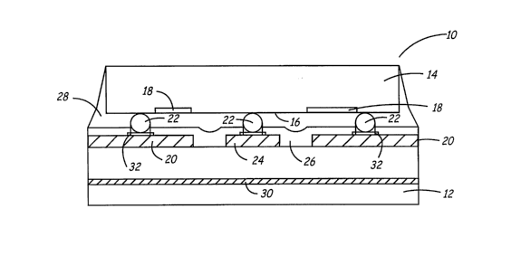
FIG. 1 illustrates an exemplary embodiment of the flip-chip component package
10
of the present invention, which is particularly beneficial in high voltage
discrete die
packages and other high voltage component packages, where "high voltage
component" or
"high voltage discrete die" is defined herein as a device that is operable
with a potential
greater than fifty (50) volts, preferably greater than one hundred (100)
volts, more
preferably greater than five hundred (500) volts, and even more preferably
greater than
one thousand (1000) or sixteen hundred (1600) volts. However, one of ordinary
skill in the
art will recognize that other die and components can be employed in packages
according
to various embodiments of the present invention, which packages can be used in
a wide
variety of applications. The component package or high voltage component
package in
accordance with the present invention may include any number of devices such
as Field
Effect Transistors (FETs), Metal Oxide Semiconductor (MOS) FETs (MOSFETs),
Insulated Gate FETs (IGFETs), thyristors, bipolar transistors, diodes, MOS-
controlled
thyristors, resistors, capacitors, etc.
Flip-chip component package 10 comprises a non-metal substrate 12 and a
component, or die, 14. Component 14 has a first surface 16 at which has been
formed at
least one field termination ring 18. Field termination zing 18 may be formed
on first
surface 16 of component 14 using any method as is known in the semiconductor
industry
including but not limited to, diffusion, implantation, and the formation of
moats.
CA 02516058 2005-08-12
WO 2004/075294 PCT/US2004/004040
4
Typically, component 14 comprises a plurality of concentric field termination
rings. Field
termination rings axe well known in the semiconductor industry and,
accordingly, will not
be described in detail here.
Flip-chip component package 10 further comprises a shield plane 20 interposed
between substrate 12 and component 14. In one exemplary embodiment of the
invention,
shield plane 20 is formed overlying substrate 12. Shield plane 20 is formed of
a
conductive material, such as, for example, a metal. In a preferred embodiment,
shield
plane 20 is formed of copper. It will be appreciated that flip-chip component
package I O
may comprise further active components or connections, such as conductive
layer 24
overlying substrate 12.
Component 14 is "flip-chip mounted" onto substrate 12. As illustrated in FIG.
1,
component 14 is formed with a plurality of solder bumps 22 connected to active
electrical
terminal connections at first surface 16. Each solder bump 22 is connected to
a solder
bonding pad 32 formed on substrate 12. In one exemplary embodiment, flip-chip
component package 10 also may comprise a solder mask layer 26, which may
overlie
shield plane 20 and may be patterned to define solderable areas, such as, for
example,
solder bonding pads 32 to which solder bumps 22 are connected. Flip-chip
component
package 10 further comprises an undertill material 28. The underfill material
28 may
comprise epoxy resin or any other material well known in the semiconductor
industry.
Without intending to be bound by theory, it is believed that, at elevated
temperatures, .
typically temperatures greater than about 80°C, underfill material 28
may begin to
approach its glass-transition temperature. Underflll material 28 may Iose
hardness, and the
molecules may be free to move or rotate within the material. This may allow
the underfill
molecules to become polarized in the presence of a strong electric field. The
mobility of
free ionic contaminants in underfill material 28 also may be increased as the
material
softens as the temperature is increased. When component 14 is in the "off
state" and a
voltage is applied across main electrical terminals, an electric field may
develop across
field termination ring 18 on the surface 16 of component 14. An electric
fringing field may
extend from the surface of component I4 into underfill material 28. The polar
components
of underfill 28 may orient themselves as dictated by the direction and
polarity of the
electric fringing field. Airy free ions may move through underfill material 28
as dictated
by the polarity of their charge and the direction of the electric fringing
field. The ions may
CA 02516058 2005-08-12
WO 2004/075294 PCT/US2004/004040
then accumulate at the surface of corriponent 14 if the electric fringing
field is applied
continuously at an elevated temperature. The additional electric field set up
by polarization
of unde~ll 28 or accumulation of ionic charge may have a negative effect on
the
performance of component 14. As underfill material 28 polarizes and the charge
, accumulates, the additional electric fields may terminate on charge carriers
in component
14 and create an inversion layer at the surface of component 14 that may form
a leakage
path across field termination ring 18. This may cause component 14 to
gradually switch
from the "off state" to the "on-state."
Shield plane 20 is configured so that there is a dominant electric field
between
component 14 and shield plane 20, rather than across field termination ring
18. The field
between component 14 and shield plane 20 may create polarization of underfill
material
28 towards shield plane 20. It also may attract ions towards shield plane 20
and away from
the surface of component 14, and generate a vertical electric field that
promotes a light
accumulation layer to form at the surface of component I4. In this manner, the
formation
of the inversion layer at the su'rface'of the substrate iraay be reduced or
eliminated, and
leakage current stability may be achieved. Accordingly, in one exemplary
embodiment of
the invention, shield plane 20 is configured to receive a biasing voltage to
produce the
electric field between component 14 and shield plane 20. The biasing voltage
preferably
has a magnitude at least as great as the magnitude of the biasing voltage
applied to
component 14, the voltages having the same polarity. For example, for a
component
package 10 with an N-type substrate, a positive biasing voltage is applied to
shield plane
20, the positive biasing voltage preferably having a magnitude at least as
great as the
magnitude of the most positive biasing voltage applied to component 14.
Similarly, for a
component package 10 having a P-type substrate, a negative biasing voltage is
applied to
shield plane 20, the negative biasing voltage preferably having a magnitude at
least as
great as the magnitude of the most negative biasing voltage applied to
component 14.
Shield plane 20 may be connected directly to a terminal of component 14 if the
component
has unidirectional blocking characteristics, such as MOSFETs and diodes.
However, if
component 14 has bidirectional blocking, such as a tliyristor, the voltage on
shield plane
20 should be switched. In either case, shield plane 20 should be biased with a
polarity that
promotes accumulation of majority carriers at the surface of the lightly doped
surface
region at the field termination ring 18.
CA 02516058 2005-08-12
WO 2004/075294 PCT/US2004/004040
6
Further, in another exemplary embodiment of the invention, shield plane 20
should
be sufficiently close to field termination ring 18 so that the electric field
between
component 14 and shield plane 20 dominates. The height of the solder bumps 22
may be
configured to provide the preferable maximum distance between field
termination ring 18
and shield plane 20. For example, a 1000V MOSFET intended to operate at 80%
rated
voltage at 125°C should have shield plane 20 within 50 to 200 wm from
the field
termination ring 18. The minimum distance between shield plane 20 and
component 14 is
determined by the dielectric strength of the insulating layers between shield
plane 20 and
component 14, such as, for example, underfill material 28 and solder mask
layer 26.
Moreover, in another exemplary embodiment of the invention, shield plane 20
has
a surface area that is at least the size of the surface area of field
termination ring 18.
Alternatively, if there is a plurality of concentric termination rings, shield
plane 20 may
have a surface area of the total annular ring comprising the concentric
termination rings. In
addition, the surface area of shield plane 20 is coextensive with the surface
area of field
termination ring 18. In a preferred embodiment of the invention, the surface
area of shield
plane 20 is coextensive with and extends beyond the surface area of field
termination ring
18 to compensation for any misalignment of component 14 when it is mounted on
substrate 12. Referring to FIG. 2, a plurality of concentric field termination
rings 40, 42,
44 forming a total annular ring 50 are illustrated in phantom overlying
substrate 12. Shield
plane 20 overlies substrate 12. 'The surface area 46 of shield plane 20 (shown
with
diagonal lines) is at least the size of the surface area 48 of total annular
ring 50 comprising
termination rings 40, 42, 44. Further, as illustrated in FIG. 2, surface area
46 of shield
plane 20 is coextensive with the surface area 48 of the total annular ring of
the field
termination rings and also extends beyond surface area 48. As used herein,
"coextensive"
means that the boundaries or edges of the surface area of the field
termination ring, or the
total annular ring, align with the boundaries of the surface area of the
shield plane or that
the boundaries of the surface area of the shield plane extend beyond the
boundaries of the
field termination ring (or total annular ring, as the case may be).
Referring again to FIG. l, in another exemplary embodiment of the invention,
flip-
chip component package 10 may further comprise a circuit trace 30 formed
within
substrate 12. Without shield plane 20, if trace 30 has a strong potential and
is in close
proximity to surface 16 of component 14, an inversion layer may form in
component 14
CA 02516058 2005-08-12
WO 2004/075294 PCT/US2004/004040
7
due to the creation of a parasitic transistor between component 14 and
substrate 12. Shield
plane 20 serves to terminate or reduce the effect of the electric fields
created at cirouit
trace 30 so that it cannot detrimentally influence the performance of
component I4.
Accordingly, it will be appreciated by those skilled in the art that shield
plane 20 may be
formed overlying substrate 12 or, alternatively, may be formed within
substrate 12 as long
as it is interposed between circuit trace 30 and component 14.
FIG. 3 illustrates a flip-chip package process in accordance with another
exemplary embodiment of the invention. A non-metal substrate is provided at
step 60. It
will be appreciated that the substrate, may comprise one layer or a plurality
of various
layers, one or more of which may be a circuit trace. In one embodiment of the
invention, a
plurality of solder bonding pads is formed on a surface of the substrate. The
solder
bonding pads can be either SMD (Solder Mask Defined) type or NSMD (Non-SMD)
type,
or mixed SMD-NSMD type. These types of bond pads are all well-known in the
semiconductor industry, so 'description thereof will not be further detailed.
A component having a field termination ring is provided at step 62. A
plurality of
~ ., .. . . , i
solder bumps is formed on a surface of the component. The component then is
flip=chip
mounted onto the substrate, as provided at step 64. The component is mounted
in an
upside-down (flip chip) manner onto the substrate, with the solder bumps
thereof being
aligned respectively to the substrate-side bonding pads. A solder-reflow
process is then
performed to reflow the solder bumps over the substrate-side bonding pads. In
an optional
step, an underfill material then may be provided, which flows by capillary
action into the
gap between the component and the substrate.
The flip-chip packaging process of the present invention further comprises
interposing a shield plane between the at least one layer of the substrate and
the field
termination ring of the component, as provided at step 66. In one exemplary
embodiment
of the invention, the shield plane may overlie the substrate. In this
embodiment, the shield
plane is disposed on the surface of the substrate before the component is flip-
chip mounted
onto the substrate. In another exemplary embodiment of the invention, the
shield plane
may be formed within the substrate as the substrate is formed and may be
interposed
i
between the field termination ring and a circuit trace formed as a layer of
the substrate. In
this embodiment, the shield plane is interposed between the field termination
ring and the
cixcuit trace before the component is flip-chip mounted onto the substrate.
CA 02516058 2005-08-12
WO 2004/075294 PCT/US2004/004040
8
Thus, there has been provided, in accordance with the invention, a flip-chip
package and a flip-chip packaging process that fully meets the needs set forth
above. The
package is compact and provides stable electrical characteristics, even at
high
temperatures. Although various embodiments of the invention have been
described and
S illustrated with reference to specific embodiments thereof, it is not
intended that the
invention be limited to such illustrative embodiments. For example, while the
invention
has been described for use with high voltage components, it will be
appreciated that the
invention may be used with any suitable electronic component. Further, while
the field
termination ring is described has having the shape of a "ring", it will be
appreciated that
the field termination ring and any corresponding "total annular ring," as used
herein, may
assume any shape that surrounds an internal active region. Moreover, while the
present
invention has been described with reference to operation of high voltage
components at
temperatures above about 80°C, the invention may be useful at
temperatures below 80°C.
Those of skill in the art will recognize that many variations and
modifications of such
embodiments are possible'without'departing from the spirit of the invention.
Accordingly,
it is intended to encompass within the invention all such modifications and
variations as
fall within the scope of the appended claims.
Benefits, other inventive aspects, and solutions to problems have been
described
above with regard to specific embodiments. However, the benefits, advantages,
solutions
to problems, and any elements) that may cause any benefit, advantage, or
solution to
occur or become more pronounced are not to be construed as a critical,
required, or
essential features or elements of any or all the claims. As used herein, the
terms
"comprises," "comprising," or any other variation thereof, are intended to
cover a non-
exclusive inclusion, such that a process, method, article, or apparatus that
comprises a list
of elements does not include only those elements but may include other
elements not
expressly listed or inherent to such process, method, article, or apparatus.