Note: Descriptions are shown in the official language in which they were submitted.
CA 02516625 2005-08-22
Internal reference: IRDM.026-2 NON-EP / IDC-040039
SYSTEM AND METHOD OF SENSING ACTUATION AND RELEASE
VOLTAGES OF AN INTERFEROMETRIC MODULATOR
Back-rg_ ound
Field
The field of the invention relates to microelectromechanical systems (MEMS).
Description of the Related Technolo~y
Microelectromechanical systems (MEMS) include micro mechanical elements,
actuators,
and electronics. Micromechanical elements may be created using deposition,
etching, and or
other micromachining processes that etch away parts of substrates and/or
deposited material
layers or that add layers to form electrical and electromechanical devices.
One type of MEMS
device is called an interferometric modulator. An interferometric modulator
may comprise a pair
of conductive plates, one or both of which may be partially transparent and
capable of relative
motion upon application of an appropriate electrical signal. One plate may
comprise a stationary
layer deposited on a substrate, the other plate may comprise a metallic
membrane suspended over
the stationary layer. Such devices have a wide range of applications, and it
would be beneficial
in the art to utilize and/or modify the characteristics of these types of
devices so that their
features can be exploited in improving existing products and creating new
products that have not
yet been developed.
S ummary
The system, method, and devices of the invention each have several aspects, no
single
one of which is solely responsible for its desirable attributes. Without
limiting the scope of this
invention, its more prominent features will now be discussed briefly. After
considering this
discussion, and particularly after reading the section entitled "Detailed
Description of Certain
Embodiments" one will understand how the features of this invention provide
advantages over
other display devices.
In one embodiment, the invention comprises a method of determining one or both
of an
actuation voltage and a release voltage of a microelectromechanical device.
The method includes
applying at least two different electric potentials to at least one electrode
coupled to the device
and detecting at least one electrical response of the device at the at least
two different electric
potentials. Based at least in part on the response, a state of the device at
the at least two different
-1-
CA 02516625 2005-08-22
electric potentials is determined. Based at least in part on the determining a
state one or both of
the actuation voltage and release voltage are determined.
In another embodiment, a system for determining one or both of an actuation
voltage and
a release voltage of a microelectromechanical device includes means for
applying at least two
different electric potentials to at least one electrode coupled to the device
and means for detecting
at least one electrical response of the device at the at least two different
electric potentials.
Additionally provided are means for determining, based at least in part on the
response, a state of
the device at the at least two different electric potentials and means for
determining one or both
of the actuation voltage and release voltage based at least in part on the
determining.
In another embodiment, a system for determining one or both of an actuation
voltage and
a release voltage of a microelectromechanical device includes a
microelectromechanical device
and a driving circuit configured to apply a voltage to the
microelectromechanical device. A
sensor connected to the a microelectromechanical device is configured for
detecting at least one
electrical response of the microelectromechanical device at the at least two
different electric
potentials. The sensor is further configured for determining, based at least
in part on the
response, a state of the device at the at least two different electric
potentials and for determining
one or both of the actuation voltage and release voltage based at least in
part on the determining.
In another embodiment, a method of manufacturing a display system includes
forming an
array of microelectromechanical pixels configured to present display data to a
user of the display
system. The method includes, forming at least one additional
microelectromechanical element;
and coupling a sensor configured to sense one or both of an actuation voltage
or a release voltage
to the additional microelectromechanical element.
In another embodiment, a display system includes an array of
microelectromechanical
pixels configured to present display data to a user of the display system, at
least one additional
microelectromechanical element, and a sensor. The sensor is configured to
sense one or both of
an actuation voltage or a release voltage of the additional
microelectromechanical pixel.
In another embodiment, a display system includes means for displaying data to
a user of a
display system and at least one microelectromechanical element. Also provided
are means for
detecting one or both of an actuation voltage or a release voltage of the
microelectromechanical
element.
In another embodiment, a method of manufacturing a system for determining one
or both
of an actuation voltage and a release voltage of a microelectromechanical
device includes
forming a microelectromechanical device and coupling a driving circuit
configured to apply a
voltage to the microelectromechanical device. The method also includes
coupling a sensor to the
a microelectromechanical device, the sensor is configured for detecting at
least one electrical
response of the microelectromechanical device at the at least two different
electric potentials, and
-2-
CA 02516625 2005-08-22
is further configured for determining, based at least in part on the response,
a state of the device
at the at least two different electric potentials. The sensor also determines
one or both of the
actuation voltage and release voltage based at least in part on the
determining.
Brief Description of the Drawings
Figure 1 is an isometric view depicting a portion of one embodiment of an
interferometric modulator display in which a movable mirror of a first
interferometric modulator
is in a reflective, or "on," position at a predetermined distance from a fixed
mirror and the
movable mirror of a second interferometric modulator is in a non-reflective,
or "off' position.
Figure 2 is a system block diagram illustrating one embodiment of an
electronic device
incorporating a 3x3 interferometric modulator display.
Figure 3A is a diagram of movable mirror position versus applied voltage for
one
exemplary embodiment of an interferometric modulator of Figure 1.
Figure 3B is an illustration of sets of row and column voltages that may be
used to drive
an interferometric modulator display.
Figure 4A illustrates one exemplary frame of display data in the 3x3
interferometric
modulator display of Figure 2.
Figure 4B illustrates one exemplary timing diagram for row and column signals
that may
be used to write the frame of Figure 4A.
Figure SA is a cross section of the device of Figure 1.
Figure SB is a cross section of an alternative embodiment of an
interferometric
modulator.
Figure SC is a cross section of an alternative embodiment of an
interferometric modulator
Figure 6 is a schematic/block diagram of one embodiment of a state sensing
circuit.
Figure 7 is graph illustrating a voltage vs. time response to a voltage pulse
for an
interferometric modulator.
Figure 8 is a schematic/block diagram of another embodiment of a state sensing
circuit
Figure 9 is graph illustrating a current vs. time response to a voltage pulse
for an
interferometric modulator.
Figure 10 is a flow chart of a state sensing process.
Figure 11 is a timing diagram illustrating row and column voltages for setting
and testing
a row of interferometric modulators.
Figure 12 is a block diagram of a state sensing apparatus for modulators
embedded in
arrays.
Figure 13 is a flow chart of another embodiment of a state sensing process.
Figure 14 is a block diagram of a display incorporating test pixels.
-3-
CA 02516625 2005-08-22
Figure 15 is a graph of voltage versus time applied to a pixel which may be
used to
determine the actuation and release voltages of an interferometric modulator.
Figure 16 is a schematic of a circuit which may be used to determine the
actuation and
release voltages used with the voltage versus time voltage application of
Figure 15.
Figure 17 is a graph illustrating the timing of the circuit of Figure 16.
Figure 18 is a graph of another embodiment of a voltage versus time applied to
a pixel
and current versus time response which may be used to determine the actuation
and release
voltages of an interferometric modulator.
Figure 19 is a schematic of a circuit which may be used to determine the
actuation and
release voltages with the voltage versus time voltage application of Figure
18.
Figure 20 is a schematic of another embodiment of a circuit which may be used
to
determine the actuation and release voltages of an interferometric modulator.
Figures 21A and 21B are system block diagrams illustrating an embodiment of a
visual
display device comprising a plurality of interferometric modulators.
Detailed Description of Preferred Embodiments
The following detailed description is directed to certain specific embodiments
of the
invention. However, the invention can be embodied in a multitude of different
ways as defined
and covered by the claims. In this description, reference is made to the
drawings wherein like
parts are designated with like numerals throughout.
Embodiments of the invention may be implemented in any device that is
configured to
display an image, whether in motion (e.g., video) or stationary (e.g., still
image), and whether
textual or pictorial. More particularly, it is contemplated that the invention
may be implemented
in or associated with a variety of electronic devices such as, but not limited
to, mobile telephones,
wireless devices, personal data assistants (PDAs), hand-held or portable
computers, electronic
books, GPS receivers/navigators, cameras, MP3 players, camcorders, game
consoles, wrist
watches, clocks, calculators, television monitors, flat panel displays,
computer monitors, auto
displays (e.g., odometer display, etc.), cockpit controls and/or displays,
display of camera views
(e.g., display of a rear view camera in a vehicle), electronic photographs,
electronic billboards or
signs, projectors, architectural structures, packaging, and aesthetic
structures (e.g., display of
images on a piece of jewelry).
MEMS devices of similar structure to those described herein can also be used
in non-
display applications such as in electronic switching devices.
One interferometric modulator display embodiment comprising an interferometric
MEMS display element is illustrated in Figure 1. In these devices, the pixels
are in either a
bright or dark state. In the bright ("on" or "open") state, the display
element reflects a large
-4-
CA 02516625 2005-08-22
portion of incident visible light to a user. When in the dark ("off ' or
"closed") state, the display
element reflects little incident visible light to the user. Depending on the
embodiment, the light
reflectance properties of the "on" and "off ' states may be reversed. MEMS
pixels can be
configured to reflect predominantly at selected colors, allowing for a color
display in addition to
black and white.
Figure 1 is an isometric view depicting two adjacent pixels in a series of
pixels of a
visual display, wherein each pixel comprises a MEMS interferometric modulator.
1n some
embodiments, an interferometric modulator display comprises a row/column array
of these
interferometric modulators. Each interferometric modulator includes a pair of
reflective layers
positioned at a variable and controllable distance from each other to form a
resonant optical
cavity with at least one variable dimension. In one embodiment, one of the
reflective layers may
be moved between two positions. In the first position, referred to herein as
the released state, the
movable layer is positioned at a relatively large distance from a fixed
partially reflective layer. In
the second position, the movable layer is positioned more closely adjacent to
the partially
reflective layer. Incident light that reflects from the two layers interferes
constructively or
destructively depending on the position of the movable reflective layer,
producing either an
overall reflective or non-reflective state for each pixel.
The depicted portion of the pixel array in Figure 1 includes two adjacent
interferometric
modulators 12a and 12b. In the interferometric modulator 12a on the left, a
movable and highly
reflective layer 14a is illustrated in a released position at a predetermined
distance from a fixed
partially reflective layer 16a. In the interferometric modulator 12b on the
right, the movable
highly reflective layer 14b is illustrated in an actuated position adjacent to
the fixed partially
reflective layer 16b.
The fixed layers 16a, 16b are electrically conductive, partially transparent
and partially
reflective, and may be fabricated, for example, by depositing one or more
layers each of
chromium and indium-tin-oxide onto a transparent substrate 20. The layers are
patterned into
parallel strips, and may form row electrodes in a display device as described
further below. The
movable layers 14a, 14b may be formed as a series of parallel strips of a
deposited metal layer or
layers (orthogonal to the row electrodes 16a, 16b) deposited on top of posts
18 and an intervening
sacrificial material deposited between the posts 18. When the sacrificial
material is etched away,
the deformable metal layers are separated from the fixed metal layers by a
defined air gap 19. A
highly conductive and reflective material such as aluminum may be used for the
deformable
layers, and these strips may form column electrodes in a display device.
With no applied voltage, the cavity 19 remains between the layers 14a, 16a and
the
deformable layer is in a mechanically relaxed state as illustrated by the
pixel 12a in Figure 1.
However, when a potential difference is applied to a selected row and column,
the capacitor
-5-
CA 02516625 2005-08-22
formed at the intersection of the row and column electrodes at the
corresponding pixel becomes
charged, and electrostatic forces pull the electrodes together. If the voltage
is high enough, the
movable layer is deformed and is forced against the fixed layer (a dielectric
material which is not
illustrated in this Figure may be deposited on the fixed layer to prevent
shorting and control the
separation distance) as illustrated by the pixel 12b on the right in Figure 1.
The behavior is the
same regardless of the polarity of the applied potential difference. In this
way, row/column
actuation that can control the reflective vs. non-reflective pixel states is
analogous in many ways
to that used in conventional LCD and other display technologies.
Figures 2 through 4B illustrate one exemplary process and system for using an
array of
interferometric modulators in a display application. Figure 2 is a system
block diagram
illustrating one embodiment of an electronic device that may incorporate
aspects of the invention.
In the exemplary embodiment, the electronic device includes a processor 21
which may be any
general purpose single- or multi-chip microprocessor such as an ARM, Pentium ,
Pentium II~,
Pentium III~, Pentium IVY', Pentium Pro, an 8051, a MIPS~, a Power PC~, an
ALPHA~, or any
other suitable processor. In addition, the processor 21 may comprise any
special purpose
microprocessor such as a digital signal processor, microcontroller, or a
programmable gate array.
As is conventional in the art, the processor 21 may be configured to execute
one or more software
modules. In addition to executing an operating system (not shown), the
processor may be
configured to execute one or more software applications, including a web
browser, a telephone
application, an email program, or any other software application. It will be
appreciated that all of
the functionality described herein may be implemented in whole or part in
hardware, software, or
a combination thereof.
In one embodiment, the processor 21 is also configured to communicate with an
array
controller 22. In one embodiment, the array controller 22 includes a row
driver circuit 24 and a
column driver circuit 26 that provide signals to the array 30. The cross
section of the array
illustrated in Figure 1 is shown by the lines 1-1 in Figure 2. The array
control 22 may also
include a boost circuit 32 for converting control signals to a voltage or
voltages sufficient for
driving the array 30. In one embodiment, the display control 22 also includes
a frame buffer 34.
The frame buffer typically includes sufficient memory to store the current
displayed frame for
refresh purposes.
A plurality of tri-state buffers 36 are advantageously provided on each of the
columns
and each of the rows of array 30. The tri-state buffers 36 are connected to
hold-mode signals
which open the connection to the respective row or column of the array when
they are asserted.
When the hold-mode select lines are asserted, lines from the driver to the
array are opened,
substantially eliminating any leakage path for the charge stored on each pixel
capacitance. The
pixels are thus held in the previously charged or discharged state without any
driver input, until
-6-
CA 02516625 2005-08-22
the charge slowly dissipates, either through leakage across the pixel or
through a non-infinite tri-
state open resistance. It will be appreciated that any controllable series
switch such as a series
FET could be used to implement this display/driver decoupling.
For MEMS interferometric modulators, the row/column actuation protocol may
take
advantage of a hysteresis property of these devices illustrated in Figure 3A.
It may require, for
example, a 10 volt potential difference to cause a movable layer to deform
from the released state
to the actuated state. However, when the voltage is reduced from that value,
the movable layer
maintains its state as the voltage drops back below 10 volts. In the exemplary
embodiment of
Figure 3A, the movable layer does not release completely until the voltage
drops below 2 volts.
There is thus a range of voltage, about 3 to 7 V in the example illustrated in
Figure 3A, where
there exists a window of applied voltage within which the device is stable in
either the released or
actuated state. This is referred to herein as the "hysteresis window" or
"stability window." For a
display array having the hysteresis characteristics of Figure 3A, the
row/column actuation
protocol can be designed such that during row strobing, pixels in the strobed
row that are to be
actuated are exposed to a voltage difference of about 10 volts, and pixels
that are to be released
are exposed to a voltage difference of close to zero volts. After the strobe,
the pixels are exposed
to a steady state voltage difference of about 5 volts such that they remain in
whatever state the
row strobe put them. After being written, each pixel sees a potential
difference within the
"stability window" of 3-7 volts in this example. This feature makes the pixel
design illustrated in
Figure 1 stable under the same applied voltage conditions in either an
actuated or released pre-
existing state. Since each pixel of the interferometric modulator, whether in
the actuated or
released state, is essentially a capacitor formed by the fixed and moving
reflective layers, this
stable state can be held at a voltage within the hysteresis window with almost
no power
dissipation. Essentially no current flows into the pixel if the applied
potential is fixed.
In typical applications, a display frame may be created by asserting the set
of column
electrodes in accordance with the desired set of actuated pixels in the first
row. A row pulse is
then applied to the row 1 electrode, actuating the pixels corresponding to the
asserted column
lines. The asserted set of column electrodes is then changed to correspond to
the desired set of
actuated pixels in the second row. A pulse is then applied to the row 2
electrode, actuating the
appropriate pixels in row 2 in accordance with the asserted column electrodes.
The row 1 pixels
are unaffected by the row 2 pulse, and remain in the state they were set to
during the row 1 pulse.
This may be repeated for the entire series of rows in a sequential fashion to
produce the frame.
Generally, the frames are refreshed and/or updated with new display data by
continually
repeating this process at some desired number of frames per second. A wide
variety of protocols
for driving row and column electrodes of pixel arrays to produce display
frames are also well
known and may be used in conjunction with the present invention.
CA 02516625 2005-08-22
Figures 3B, 4A and 4B illustrate one possible actuation protocol for creating
a display
frame on the 3x3 array of Figure 2. Figure 3B illustrates a possible set of
column and row
voltage levels that may be used for pixels exhibiting the hysteresis curves of
Figure 3A. In the
Figure 3B embodiment, actuating a pixel involves setting the appropriate
column to -V6;es, and
the appropriate row to +~V, which may correspond to -5 volts and +5 volts
respectively
Releasing the pixel is accomplished by setting the appropriate column t0
+Vb;as, and the
appropriate row to the same +0V, producing a zero volt potential difference
across the pixel. In
those rows where the row voltage is held at zero volts, the pixels are stable
in whatever state they
were originally in, regardless of whether the column is at +Vb;as, or -Vb;as~
Figure 4B is a timing diagram showing a series of row and column signals
applied to the
3x3 array of Figure 2 which will result in the display arrangement illustrated
in Figure 4A, where
actuated pixels are non-reflective. Prior to writing the frame illustrated in
Figure 4A, the pixels
can be in any state, and in this example, all the rows are at 0 volts, and all
the columns are at +5
volts. With these applied voltages, all pixels are stable in their existing
actuated or released
states.
In the Figure 4A frame, pixels (1,1), (1,2), (2,2), (3,2) and (3,3) are
actuated. To
accomplish this, during a "line time" for row 1, columns 1 and 2 are set to -5
volts, and column 3
is set to +5 volts. This does not change the state of any pixels, because all
the pixels remain in
the 3-7 volt stability window. Row 1 is then strobed with a pulse that goes
from 0, up to 5 volts,
and back to zero. This actuates the (1,1) and (1,2) pixels and releases the
(1,3) pixel. No other
pixels in the array are affected. To set row 2 as desired, column 2 is set to -
5 volts, and columns
1 and 3 are set to +5 volts. The same strobe applied to row 2 will then
actuate pixel (2,2) and
release pixels (2,1) and (2,3). Again, no other pixels of the array are
affected. Row 3 is similarly
set by setting columns 2 and 3 to -5 volts, and column 1 to +5 volts. The row
3 strobe sets the
row 3 pixels as shown in Figure SA. After writing the frame, the row
potentials are zero, and the
column potentials can remain at either +5 or -5 volts, and the display is then
stable in the
arrangement of Figure 4A. It will be appreciated that the same procedure can
be employed for
arrays of dozens or hundreds of rows and columns. It will also be appreciated
that the timing,
sequence, and levels of voltages used to perform row and column actuation can
be varied widely
within the general principles outlined above, and the above example is
exemplary only, and any
actuation voltage method can be used with the present invention.
The details of the structure of interferometric modulators that operate in
accordance with
the principles set forth above may vary widely. For example, Figures SA-SC
illustrate three
different embodiments of the moving mirror structure. Figure SA is a cross
section of the
embodiment of Figure 1, where a strip of metal material 14 is deposited on
orthogonally
extending supports 18. In Figure SB, the moveable reflective material 14 is
attached to supports
_g_
CA 02516625 2005-08-22
at the corners only, on tethers 38. In Figure SC, the moveable reflective
material 14 is suspended
from a deformable layer 40. This embodiment has benefits because the
structural design and
materials used for the reflective material 14 can be optimized with respect to
the optical
properties, and the structural design and materials used for the deformable
layer 40 can be
optimized with respect to desired mechanical properties. The production of
various types of
interferometric devices is described in a variety of published documents,
including, for example,
U.S. Published Application 2004/0051929. A wide variety of well known
techniques may be
used to produce the above described structures involving a series of material
deposition,
patterning, and etching steps.
After a pixel is written, it can be advantageous to sense its state. For the
bi-stable display
of Figure 1, the state of a pixel can be determined by taking advantage of the
fact that the
capacitance across the pixel mirrors is much larger, often about ten times
larger, when the pixels
are in the actuated state than when they are in the released state. This pixel
capacitance value can
be sensed in a variety of ways by sensing capacitance dependent electrical
properties of the pixel,
some of which are described in more detail below.
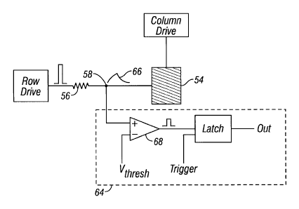
The principles of pixel state sensing will be described first with reference
to a single
pixel in isolation as illustrated in Figures 6-10. Referring now to Figure 6,
after pixel writing,
whether the whole frame is complete or prior to that time, all the column tri-
state buffers can be
placed in the open (decoupled) configuration except one column containing the
pixel to be tested.
The row driver then applies a low amplitude pulse to the row electrode
containing the pixel to be
tested, which charges up in response to the increased voltage. As shown in
Figure 7, the voltage
across the pixel will increase in response to this applied voltage in
accordance with the RC time
constant (i) of the circuit. For a single pixel in isolation, the capacitance
is the capacitance of the
pixel 54, and the resistance of the circuit may include the row driver output
impedance and/or any
filter resistor 56 that might be placed in series with the row electrode. The
voltage at the test
point 58 when the pixel 54 is in a low capacitance state (e.g. in the released
state) will increase
faster as illustrated by curve 60 than when the pixel 54 is in a high
capacitance state (e.g. in the
actuated state) as illustrated by curve 62. If the voltage across the pixel is
determined at a certain
time during this charging period, at i/3 for example, the state of the pixel
can be determined.
This voltage can be detected and measured by a voltage sensing circuit 64. If
a pulse having a
duration of i/3 is applied to the pixel, the voltage across the pixel will
increase and decrease as
shown in the trace 66 (also shown in Figure 7). If this signal is applied to
the input of a
comparator 68 with Vt,~esn applied to the negative input, a pulse will be
output from the
comparator only if the voltage across the pixel exceeded V~,,resn at some time
during the pulse,
where V~hresh ~S defined as shown in Figure 7. The output of the comparator 68
can be latched to
produce an indication of whether that pixel is actuated (latch low) or
released (latch high).
-9-
CA 02516625 2005-08-22
Figures 8 and 9 illustrate an alternative method of detecting pixel state. In
Figure 8, a
current sensing circuit 70 is used rather than a voltage sensing circuit. A
voltage pulse is applied
as above, which causes a current pulse as the pixel capacitance charges. As
illustrated in Figure
9, this current pulse decays slower (curve 75) for a larger capacitance of
pixel 54 than for a
smaller capacitance (curve 77). The current pulse can be converted to a
voltage pulse by
measuring the voltage across a series resistance 72 in the column line
(amplifiers configured as
current to voltage converters could also be used). The voltage across the
resistor can be sensed
by an amplifier configured as an integrator 74 illustrated in Figure 8. The
output of the integrator
can be routed to a similar comparator 76 and latch as in Figure 6. The
comparator 76 will only
produce an output pulse if the current pulse through the circuit is sufficient
(given the value of
the resistor 72 and the time constant/amplification of the integrator 74) to
produce a voltage at
the comparator input greater than a threshold voltage Vr,,~es,~ shown in
Figure 8. Figure 8 shows a
switch 78 used to switch resistance 72 into the column line, but it will be
appreciated that this
would not be necessary if a suitable filter resistor, for example, was already
present.
Current sensing requires a slightly more complicated circuit than voltage
sensing, but one
advantage would be that all the pixels in a row could be probed by a single
pulse since the
charging current could be separately measured for each pixel along a row
simultaneously with
separate current sensors. In these embodiments, there may be a sensor
dedicated to each column,
or a set of current sensors could be sequentially switched between different
groups of columns
such that a portion, but not all of the column currents are sensed
concurrently. This last
embodiment would be slower than an embodiment with a sensor for every row, but
faster than
one at a time sensing.
In accordance with the principles above, Figure 10 is a flowchart illustrating
an
exemplary process for determining an open or closed state of an
interferometric modulator. A
test pulse is applied to the pixel at step 80. At step 82, a capacitance
dependent response to the
pulse is measured. At step 84, the response is compared to a threshold to
determine the state of
the pixel.
Pixel state sensing can be advantageous for a variety of reasons. For example,
on the
next frame update or refresh, only those pixels that are different from the
next desired frame need
be updated. For a static display, the pixel states may be monitored to detect
which pixels have
relaxed from an actuated state to a released state due to charge leakage.
Selective updating could
be performed in a variety of ways. For example, once one or more pixels change
from the
desired state, the driver circuitry could be turned back on, the tri-state
buffers closed, and row
strobing could be limited to only those rows which include pixels in an
undesired state. Other
rows could be skipped. This reduces the total energy required to update the
display. Pixel state
sensing could also be advantageous during the frame writing process, because
as rows of pixels
-10-
CA 02516625 2005-08-22
are written, they could be checked to determine if they were written correctly
or not. If not, the
row could be written again until correct. Pixel state sensing can also
advantageously minimize
the peak memory requirements for the frame buffer.
An implementation of this last process is illustrated in Figure 11. After
writing row 1
during the row 1 line time 90, a row 1 test time 92 is entered. In the first
portion of this time
period, only row 1 and column 1 are connected to the drive circuitry, and a
test pulse 94 of about
1 volt or less is applied to row 1. As described above, the capacitance
dependent response of
pixel (1,1) is monitored to be sure it is in the actuated state as shown in
Figure 5A. This is
repeated for pixels (1,2) and (1,3) during subsequent portions of the row 1
test time. The system
then enters the row 2 line time, or alternatively, repeats the row 1 line time
if it is determined that
one or more pixels in row 1 have not been correctly written. For purposes of
illustration, the test
voltage amplitude is shown larger than generally desired and the test time
period is shown much
longer than would normally be necessary, as the pulse time periods for testing
can be very short
compared to the pulse periods used to actuate the pixels during the write
process. When the pixel
54 being tested is part of a large array of tightly packed pixels, the testing
process may be
somewhat more complex. This is because the test pulse is applied to an entire
row of pixels.
Thus, the time constant of the charging process is dependent on the
capacitance between the
entire row electrode and the return column electrode, and this can be affected
by the relative
states of all the pixels in the row, not j ust on the state of the pixel being
tested 54, shown again in
Figure 12. The dominant factor in the capacitance will be the state of the
pixel being tested, but
since there may be hundreds of pixels in the row, the combined effect of the
remainder can be
significant. There can also be capacitive coupling between pixels in different
rows that share the
same column electrode. The practical effect of this is that it may be
advantageous to vary the
pulse time period T/3, the V~,"esn value, or both, when testing pixels in a
given row, depending on
the states of the other pixels in the row.
This determination can be done in several ways. One embodiment illustrated in
Figure
12 can include in each row, at the end of the row outside the viewed area of
the display, a test
pixel 98. This pixel can be switched between states, and the rise times for
the test pulse can be
determined for both the actuated and released states. In this way, the time
period having the
maximum voltage difference between states, and the voltage values between
which V~,,~esn should
be located could be determined based on the test pixel response. These values
could then be used
to test the state of the other pixels in the row.
Alternatively, a filter resistor could be placed at the end of the row instead
of a test pixel.
A collective capacitance measurement for the whole row electrode could then be
made. The
drive control circuitry could use this information to compute or look up an
appropriate value for
i/3, Vr,,~esh, or both, to test the pixels in that row.
-11-
CA 02516625 2005-08-22
A general state sensing process using these principles for pixels embedded in
arrays of
rows and columns is illustrated in Figure 13. At step 102, row measurement
signals are applied
to a row containing a pixel to be sensed. These signals could involve testing
a test pixel or an
overall row capacitance measurement as described above. At step 104,
appropriate test
S parameters such as period i/3 and/or V,~,~esn are determined for later pixel
testing in the row. As in
Figure 10, a test pulse is then applied to the row at step 106. At step 108, a
capacitance
dependent response to the pulse is measured. At step 110, the response is
compared to a
threshold to determine the state of a selected pixel in the row.
Pulse amplitudes and durations for the pixel state sensing process may be
selected based
on a variety of desired factors. The pulse may be shaped to control the total
charge injected into
the row. For isolated pixels, the pulse current and time profile can be
defined such that a pre
selected charge is injected into the pixel regardless of its capacitance
value. In this case, the
resulting voltage across the pixel will be inversely proportional to the pixel
capacitance. It may
be possible to use this method for pixels in an array as well, but its
usefulness may be limited
since the charge injected into the row may be distributed throughout the
hundreds of row pixels
in a way that is complicated and difficult to predict. Pulse durations may be
selected based on
the circuit i value, with short pulses preferred for time savings. It is of
course desirable that the
potential applied to the pixel during this process remains at all times within
the hysteresis
window so that the state sensing process does not itself change the state of
the pixel being sensed.
Thus, the driver will advantageously supply the appropriate bias voltage when
not applying a
charging pulse and when not decoupled by the tri-state amplifiers, and will
generate pulses
deviating from this bias voltage that are small enough (e.g. no more than 1 or
2 volts typically)
such that the applied pixel voltages are never outside of the hysteresis
window.
Another advantageous application of pixel state sensing is for determining the
actuation
and release voltages of a pixel. This can be useful because these voltages are
temperature
dependent, and may shift over time as well. Higher temperatures tend to shift
the stability
window of Figure 3A closer to zero for metal mirrors on glass substrates.
Depending on the
relative coefficients of thermal expansion of the material layers, shifts of
either direction as a
function of temperature can occur. If pixel actuation and release voltages can
be determined
electrically, the drive voltages used to write image data to an array of
pixels can be modified to
match the current pixel behavior. A display incorporating this feature is
illustrated in Figure 14.
In this embodiment, extra test pixels 112 are placed around the actual viewing
area of the display
114. These test pixels may be fabricated during the same process that produces
the display so
that the physical characteristics are similar if not essentially identical
with the physical
characteristics of the pixels in the viewed display area 114. One or more
sense circuits 118 that
-12-
CA 02516625 2005-08-22
apply variable bias voltages and test voltages are coupled to the test pixels.
It will be appreciated
that some or all of the sense circuitry could be shared among multiple test
pixels.
With separate test pixels, a variety of sensing protocols can be implemented
to determine
the actuation and/or the release voltages of a capacitive MEMS pixel. For
example, this
determination can be performed by applying a series of voltages across a
pixel, and sensing the
state at each applied voltage. This is illustrated in Figure 15. The voltage
can be stepped up
from zero to a voltage that is above the expected actuation voltage under all
conditions. At each
voltage level, a pixel state test as described above may be performed to
determine the pixel state.
At some voltage level, the pixel will actuate, and this will be detected
during the test. Pixel
voltage can then be stepped down and tested at each level back down to zero.
At some voltage
level, the pixel will release, and this will again be detected by the test
results.
In Figure 15, the voltage step is one volt for each step, but it will be
appreciated that any
step size may be used. During each step, after the pixel has charged from the
previous voltage
transition, a test pulse 120 is applied as described above. The appropriate
voltages or currents are
monitored as desired, and the pixel state is determined at each voltage level.
Ranges for the
actuation and release voltages can be determined by determining which step
caused a state
change. Advantageously, the amplitude and duration of the test pulses are less
than the step size
and duration.
Figures 16 and 17 illustrate a circuit and its operation that can implement
the method of
Figure 15. In this embodiment, a test pulse is added to a series of stepped up
and stepped down
voltages and the signal sum is applied to one side of a pixel. The other side
is grounded with an
inverting current to voltage converter 124. A switch 126 connects the output
of the current to
voltage converter to the input of a comparator 128. As shown in Figure 17, the
CLK 1 signal
attached to the test pulse generator produces the test pulse duration. As
illustrated in Figure 9
and described above, the test pulse produces a current pulse through the test
pixel that decays
much slower for an actuated pixel than for a released pixel. The CLK2 signal
controls the
connection between the output of the current to voltage converter 124 and the
input to the
comparator 128. The input to the comparator is pulled low by resistor 130 when
the switch 126
is open. The CLK2 signal is timed to have a rising edge delayed from the
rising edge of CLK1
and have a short duration to sample the voltage output from the current to
voltage converter 124
at a selected point in time during the charging process. This voltage will be
higher for an
actuated pixel than for a released pixel. If the voltage is more negative than
-Vthresh3 (negative
because of the inverting amplifier 124) during the CLK2 sample period, this
indicates an actuated
pixel, and the output of the comparator 128 will be high during the sample
period. This is
repeated sequentially for each test pulse, and the series of comparator
outputs are shifted into a
shift register 136 at times determined by signal CLK3 which is within the
assertion time of
-13-
CA 02516625 2005-08-22
CLK2. The outputs of the shift register 136 then form a record of the actuated
vs. released state
of the pixel at each level on the way up and back down.
Figures 18 and 19 illustrate another circuit implementation that can be used
to determine
actuation and release voltages of a bistable pixel. If the voltage on the
pixel is increased at a rate
that is slow compared to the pixel RC charging time constant and the time it
takes for a pixel to
switch between states, the current will be very low while the voltage is
ramped up. This will be
true until the pixel changes to the actuated state and the capacitance quickly
increases. This will
cause a current pulse to flow during the transition to a high capacitance
state. On the ramp back
downward, a second current pulse in the opposite direction (quickly reducing
the charge on the
pixel capacitance) will occur.
These current pulses can be detected by the circuit of Figure 19. In this
embodiment, the
output of the current to voltage converter 124 is coupled to a pair of
comparators 140 and 142.
Both comparator outputs will both be low when the charging current is small.
During the first
current pulse, the output of comparator 140 will go high. During the second
current pulse, the
output of comparator 142 will go high. The time at which these pulses occur
can be determined
by having each output pulse from the comparators stop a respective counter
144, 146 that is
started at the same time the ramp is started. The counter values can be
associated with the
actuation and release voltages because the voltage as a function of time of
the applied voltage
ramp is known.
Another possible test circuit is illustrated in Figure 20. In this embodiment,
an AC signal
is placed on top of a DC bias voltage and is applied to the pixel at node 150.
More AC current
will flow through the pixel when the pixel is actuated than when it is
released. This AC current
can be detected by including both a DC coupled path to ground and an AC
coupled path to
ground on the other plate of the pixel. The DC voltage across capacitor 154
will increase with
increasing AC current through the pixel and through capacitor 156. This
voltage is routed to a
comparator 158, which goes high if this value is above Vthresh6, which is
determined based on
the component values. In this embodiment, the DC bias voltage can be varied in
any manner, and
the output 160 of the comparator 158 will be high when the pixel is actuated,
and low when the
pixel is released.
Figures 21A and 21B are system block diagrams illustrating an embodiment of a
display
device 2040. The display device 2040 can be, for example, a cellular or mobile
telephone.
However, the same components of display device 2040 or slight variations
thereof are also
illustrative of various types of display devices such as televisions and
portable media players.
The display device 2040 includes a housing 2041, a display 2030, an antenna
2043, a
speaker 2045, an input device 2048, and a microphone 2046. The housing 2041 is
generally
formed from any of a variety of manufacturing processes as are well known to
those of skill in
-14-
CA 02516625 2005-08-22
the art, including injection molding, and vacuum forming. In addition, the
housing 2041 may be
made from any of a variety of materials, including but not limited to plastic,
metal, glass, rubber,
and ceramic, or a combination thereof. In one embodiment the housing 2041
includes removable
portions (not shown) that may be interchanged with other removable portions of
different color,
or containing different logos, pictures, or symbols.
The display 2030 of exemplary display device 2040 may be any of a variety of
displays,
including a bi-stable display, as described herein. In other embodiments, the
display 2030
includes a flat-panel display, such as plasma, EL, OLED, STN LCD, or TFT LCD
as described
above, or a non-flat-panel display, such as a CRT or other tube device, as is
well known to those
of skill in the art. However, for purposes of describing the present
embodiment, the display 2030
includes an interferometric modulator display, as described herein.
The components of one embodiment of exemplary display device 2040 are
schematically
illustrated in Figure 21 B. The illustrated exemplary display device 2040
includes a housing 2041
and can include additional components at least partially enclosed therein. For
example, in one
embodiment, the exemplary display device 2040 includes a network interface
2027 that includes
an antenna 2043 which is coupled to a transceiver 2047. The transceiver 2047
is connected to the
processor 2021, which is connected to conditioning hardware 2052. The
conditioning hardware
2052 may be configured to condition a signal (e.g. filter a signal). The
conditioning hardware
2052 is connected to a speaker 2045 and a microphone 2046. The processor 2021
is also
connected to an input device 2048 and a driver controller 2029. The driver
controller 2029 is
coupled to a frame buffer 2028 and to the array driver 2022, which in turn is
coupled to a display
array 2030. A power supply 2050 provides power to all components as required
by the particular
exemplary display device 2040 design.
The network interface 2027 includes the antenna 2043 and the transceiver 2047
so that
the exemplary display device 2040 can communicate with one or more devices
over a network.
In one embodiment the network interface 2027 may also have some processing
capabilities to
relieve requirements of the processor 2021. The antenna 2043 is any antenna
known to those of
skill in the art for transmitting and receiving signals. In one embodiment,
the antenna transmits
and receives RF signals according to the IEEE 802.11 standard, including IEEE
802.11(a), (b), or
(g). In another embodiment, the antenna transmits and receives RF signals
according to the
BLUETOOTH standard. In the case of a cellular telephone, the antenna is
designed to receive
CDMA, GSM, AMPS or other known signals that are used to communicate within a
wireless cell
phone network. The transceiver 2047 pre-processes the signals received from
the antenna 2043
so that they may be received by and further manipulated by the processor 2021.
The transceiver
2047 also processes signals received from the processor 2021 so that they may
be transmitted
from the exemplary display device 2040 via the antenna 2043.
-15-
CA 02516625 2005-08-22
In an alternative embodiment, the transceiver 2047 can be replaced by a
receiver. In yet
another alternative embodiment, network interface 2027 can be replaced by an
image source,
which can store or generate image data to be sent to the processor 2021. For
example, the image
source can be a digital video disc (DVD) or a hard-disc drive that contains
image data, or a
software module that generates image data.
Processor 2021 generally controls the overall operation of the exemplary
display device
2040. The processor 2021 receives data, such as compressed image data from the
network
interface 2027 or an image source, and processes the data into raw image data
or into a format
that is readily processed into raw image data. The processor 2021 then sends
the processed data
to the driver controller 2029 or to frame buffer 2028 for storage. Raw data
typically refers to the
information that identifies the image characteristics at each location within
an image. For
example, such image characteristics can include color, saturation, and gray-
scale level.
In one embodiment, the processor 2021 includes a microcontroller, CPU, or
logic unit to
control operation of the exemplary display device 2040. Conditioning hardware
2052 generally
IS includes amplifiers and filters for transmitting signals to the speaker
2045, and for receiving
signals from the microphone 2046. Conditioning hardware 2052 may be discrete
components
within the exemplary display device 2040, or may be incorporated within the
processor 2021 or
other components.
The driver controller 2029 takes the raw image data generated by the processor
2021
either directly from the processor 2021 or from the frame buffer 2028 and
reformats the raw
image data appropriately for high speed transmission to the array driver 2022.
Specifically, the
driver controller 2029 reformats the raw image data into a data flow having a
raster-like format,
such that it has a time order suitable for scanning across the display array
2030. Then the driver
controller 2029 sends the formatted information to the array driver 2022.
Although a driver
controller 2029, such as a LCD controller, is often associated with the system
processor 2021 as a
stand-alone Integrated Circuit (IC), such controllers may be implemented in
many ways. They
may be embedded in the processor 2021 as hardware, embedded in the processor
2021 as
software, or fully integrated in hardware with the array driver 2022.
Typically, the array driver 2022 receives the formatted information from the
driver
controller 2029 and reformats the video data into a parallel set of waveforms
that are applied
many times per second to the hundreds and sometimes thousands of leads coming
from the
display's x-y matrix of pixels.
In one embodiment, the driver controller 2029, array driver 2022, and display
array 2030
are appropriate for any of the types of displays described herein. For
example, in one
embodiment, driver controller 2029 is a conventional display controller or a
bi-stable display
controller (e.g., an interferometric modulator controller). In another
embodiment, array driver
-16-
CA 02516625 2005-08-22
2022 is a conventional driver or a bi-stable display driver (e.g., an
interferometric modulator
display). In one embodiment, a driver controller 2029 is integrated with the
array driver 2022.
Such an embodiment is common in highly integrated systems such as cellular
phones, watches,
and other small area displays. In yet another embodiment, display array 2030
is a typical display
array or a bi-stable display array (e.g., a display including an array of
interferometric
modulators).
The input device 2048 allows a user to control the operation of the exemplary
display
device 2040. In one embodiment, input device 2048 includes a keypad, such as a
QWERTY
keyboard or a telephone keypad, a button, a switch, a touch-sensitive screen,
a pressure- or heat-
sensitive membrane. In one embodiment, the microphone 2046 is an input device
for the
exemplary display device 2040. When the microphone 2046 is used to input data
to the device,
voice commands may be provided by a user for controlling operations of the
exemplary display
device 2040.
Power supply 2050 can include a variety of energy storage devices as are well
known in
the art. For example, in one embodiment, power supply 2050 is a rechargeable
battery, such as a
nickel-cadmium battery or a lithium ion battery. In another embodiment, power
supply 2050 is a
renewable energy source, a capacitor, or a solar cell, including a plastic
solar cell, and solar-cell
paint. In another embodiment, power supply 2050 is configured to receive power
from a wall
outlet.
In some implementations control programmability resides, as described above,
in a driver
controller which can be located in several places in the electronic display
system. In some cases
control programmability resides in the array driver 2022. Those of skill in
the art will recognize
that the above-described optimization may be implemented in any number of
hardware and/or
software components and in various configurations.
While the above detailed description has shown, described, and pointed out
novel
features of the invention as applied to various embodiments, it will be
understood that various
omissions, substitutions, and changes in the form and details of the device or
process illustrated
may be made by those skilled in the art without departing from the spirit of
the invention. As one
example, it will be appreciated that the test voltage driver circuitry could
be separate from the
array driver circuitry used to create the display. As with current sensors,
separate voltage sensors
could be dedicated to separate row electrodes. The scope of the invention is
indicated by the
appended claims rather than by the foregoing description. All changes which
come within the
meaning and range of equivalency of the claims are to be embraced within their
scope.
-17-