Note: Descriptions are shown in the official language in which they were submitted.
CA 02516706 2005-08-19
WO 2004/075398 PCT/GB2003/004507
1
HIGH EFFICIENCY AMPLIFICATION
Field of the Invention
The present invention relates to the control of a supply voltage , in an
arrangement in which the supply voltage is selectable. The invention is
particularly
but not exclusively concerned with the control of a supply voltage to an
amplifier such
as a broadband radio frequency (RF) amplifier having a wide dynamic range.
Background to the Invention
Transistor amplifiers have a peak efficiency for a particular input power that
is
a function of geometry (i.e. circuit components and layout), load and supply
voltage.
In conventional radio frequency (RF) power amplification these characteristics
are
fixed based on the peak input level expected. For amplifiers presented with an
input
signal having a wide dynamic range, the input signal infrequently achieves
peak
levels and frequently operates below peak levels. As such, the amplifier may
exhibit
low overall efficiency.
A solution to the problem of low amplifier efficiency is to vary one or more
of
the above-stated characteristics (geometry, load, supply voltage) in response
to the
input signal. Techniques to vary one or more of these characteristics are
known in
the art.
Techniques that vary the device geometry and load tend to be very dependent
on the particular power amplifier topology used, and generally present
challenging
RF problems. Repeatability of such designs in production is generally a
problem.
Various techniques are known in the art for enhancing amplifier efficiency
based on the supply voltage. Of supply voltage based efficiency enhancement
schemes, there are two broad classifications of solution. These solutions are:
(i) envelope elimination and restoration, and
(ii) envelope tracking.
Envelope elimination and restoration requires the amplifier to be driven
saturated, and all the envelope information to be applied through the
amplifier supply.
CA 02516706 2005-08-19
WO 2004/075398 PCT/GB2003/004507
2
This technique tends to be generally too demanding upon the supply modulator
when
using high modulation bandwidths, and thus has limited usefulness in practical
applications.
With envelope tracking, the amplifier is driven in a substantially linear
fashion.
Envelope tracking requires an efficient power supply capable of delivering
high
modulation power bandwidths. In known techniques, a switched mode pulse width
modulator (commonly referred to as class S) is used to realise an efficient
variable
supply to the power amplifier. However, in order to operate at full bandwidth,
the
supply must switch_at manytirnes the bandwidth of the modulation;"and this
excessively high switching speed results in poor modulator efficiency.
In another prior art envelope tracking technique, a plurality of highly
efficient
intermediate power supplies are provided, and the power supplies are switched
as
required by the envelope level. This switching creates transient disturbances
that
degrade the spectrum with high order intermodulation products, and makes
linearisation difficult by introducing supply dependent non-linearities
alongside input
dependent non-linearities.
In- a further modification to this technique, the switching of the power
supplies
is combined with a linear amplifier to provide a smooth transition between
switch
levels and remove the supply dependent linearisation requirement. The aim of
this
form of envelope tracking is to provide a unique value of supply voltage for
every
envelope level. However, there is a problem in achieving this without impact
upon
tracking speed capability.
It is an aim of the present invention to provide an improved supply voltage
based efficiency enhancement scheme, which preferably addresses one or more of
the above-stated problems.
Summary of the Invention
According to the present invention there is provide a power supply stage,
comprising: reference means for providing a reference signal representing a
desired
power supply voltage; election means for selecting one of a plurality of power
supply
voltages in dependence on the reference signal; adjusting means for receiving
the
selected power supply voltage and the reference signal and adapted to generate
an
CA 02516706 2005-08-19
WO 2004/075398 PCT/GB2003/004507
3
adjusted selected power supply voltage tracking the reference signal in
dependence
thereon.
The power supply stage may be for an amplifier, the reference signal
representing the envelope of an input signal of said amplifier.
The adjusting means may include an AC amplifier. The selected power supply
voltage may have the minimum absolute difference between said power supply
voltage and the reference signal level.
The -ac amplifier may - be-- connected to amplify- the--difference between the
reference signal and a representation of the selected power supply voltage.
The
adjusting means may include means for summing the amplified difference with
the
selected supply voltage.
.The representation of the selected power supply voltage may be the power
supply voltage itself. The representation of the selected power supply voltage
may be
the adjusted selected power supply voltage. The adjusted selected supply
voltage
may be the output of the power supply stage.
The adjusting means may further include a high frequency amplifier. The high
frequency amplifier may be connected to amplify the difference between the
reference signal and a representation of the adjusted power supply voltage.
The
adjusting. means may include means for summing the amplified difference with
the
adjusted supply voltage to generate a further adjusted supply voltage. The
representation of the adjusted supply voltage may be the adjusted supply
voltage
itself. The representation of the adjusted supply voltage may be the further
adjusted
supply voltage. The further adjusted supply voltage may form the output of the
power
supply stage.
There may further be provided an interpolation means at the input to the
adjusting
means such that the selected power supply voltage is interpolated. The
interpolation
means comprises an inductor-capacitor arrangement.
CA 02516706 2005-08-19
WO 2004/075398 PCT/GB2003/004507
4
There may further be provided means for DC clamping the AC amplifier. The
means for DC clamping may be responsive to detection of the reference signal
being
less than the adjusted supply voltage.
There may be provided a delay element for delaying the reference signal. There
may further be provided slow DC adjustment means for removing a DC component
from the AC amplifier.
The adjusting means may comprise a plurality of cascaded correction circuits.
.The adjusting, means may comprise two or more cascaded correction.circuits,_
There may be provided a delay element for compensating for differences in
delays between the signal amplifier and power supply control input.
In a further aspect the present invention provides a radio frequency
amplification
stage comprising: an amplifier for receiving an input signal to be amplified
and a
power supply voltage; and a power supply voltage stage for supplying said
power
supply voltage, comprising: means for providing a reference signal
representing the
envelope of the input signal; means for selecting one of a plurality of supply
voltage
levels in dependence on the reference signal; and means for generating an
adjusted
selected power supply voltage, comprising an AC amplifier for amplifying a
difference
between the reference signal and one of the selected supply voltage level or
the
adjusted selected supply voltage level, and a summer for summing the amplified
difference with the selected supply voltage to thereby generate the adjusted
supply
voltage.
The means for generating an adjusted selected supply voltage may further
generate a further adjusted supply voltage and further comprises an RF
amplifier for
amplifying a difference between the reference signal and one of the adjusted
supply
voltage or the further adjusted supply voltage, and a summer for summing such
amplified difference with the adjusted supply voltage to thereby generate the
further
adjusted supply voltage.
One of the adjusted supply voltage or further adjusted supply voltage may form
the supply voltage to the amplifier.
CA 02516706 2010-01-29
In a still further aspect the present invention provides a method of
controlling a power
supply stage, comprising: providing a reference signal representing a desired
power supply
voltage; selecting one of a plurality of power supply voltages in dependence
on the reference
signal; generating an adjusted selected power supply voltage tracking the
reference signal in
dependence on the selected power supply voltage and the reference signal.
The reference signal may represent the envelope of an input signal to an
amplifier, the
power supply stage providing a power supply to said amplifier. The difference
between the
reference signal and a representation of the selected power supply voltage may
be AC
amplified. The amplified difference may be summed with the selected supply
voltage to form
the adjusted supply voltage. The difference between the reference signal and a
representation
of the adjusted power supply voltage may be RF amplified.
The amplified difference may be summed with the adjusted supply voltage to
form a
further adjusted supply voltage. The method may further comprise an
interpolating step prior
to said step of generating an adjusted supply voltage. The method may further
comprise an
AC amplification step.
The present invention provides a controlled voltage source for maintaining a
supply
current, connected in series with the supply voltage source, such that the
same current flows
through both voltage sources.
The invention in one broad aspect provides a power supply stage, comprising:
a. reference means for providing a reference signal representing a desired
power supply
voltage; b. selection means for selecting one of a plurality of power supply
voltages in
dependence on the reference signal, the selection means being adapted for
tracking above and
below the reference signal; c. adjusting means adapted to generate an adjusted
selected power
supply voltage tracking the reference signal in dependence on the selected
power supply
voltage and the reference signal.
CA 02516706 2010-01-29
5A
Further the invention provides a radio frequency amplification stage
comprising: a. an
amplifier for receiving an input signal to be amplified and a power supply
voltage; and b. a
power supply voltage stage for supplying said power supply voltage,
comprising: i. means for
providing a reference signal representing a desired power supply voltage
corresponding to the
envelope of the input signal; ii. means for selecting one of a plurality of
supply voltage levels
in dependence on the reference signal, the means for selecting being adapted
for tracking above
and below the reference signal; and iii. means for generating an adjusted
selected power supply
voltage comprising an AC amplifier for amplifying a difference between the
reference signal
and one of the selected supply voltage level or the adjusted selected supply
voltage level, and
a summer for summing the amplified difference with the selected supply voltage
to thereby
generate the adjusted supply voltage.
Further still the inventor provides a method of controlling a power supply
stage,
comprising: a. providing a reference signal representing a desired power
supply voltage; b.
selecting one of a plurality of power supply voltages in dependence on the
reference signal,
the selecting step being adapted for tracking above and below the reference
signal; c.
generating an adjusted selected power supply voltage tracking the reference
signal in
dependence on the selected power supply voltage and the reference signal.
Brief Description of the Drawings
The present invention is now described by way of example with reference to the
accompanying Figures, in which:-
Fig. 1 illustrates a block diagram of an RF amplification stage embodying the
concept
of the present invention;
CA 02516706 2005-08-19
WO 2004/075398 PCT/GB2003/004507
6
Fig. 2(a) illustrates the concept of envelope tracking supply voltage
variation,
and the problems associated therewith;
Fig. 2(b) illustrates the principle of the improvements offered by the present
invention;
Fig. 3 illustrates in more detail an implementation of the RF amplification
stage
of Fig. 1 including a correction path in accordance with the present
invention;
Fig. 4 illustrates an enhanced exemplary implementation of the correction path
of Fig. 1;
Figs. 5(a) and 5(b) illustrate alternative implementations of the correction
path
in embodiments of the present invention;
Fig. 6 illustrates an exemplary implementation of the DC control loops of the
RF amplification stage of Fig. 1;
Fig. 7 illustrates a principle of operation in a preferred embodiment of the
invention.
Fig. 8 illustrates an exemplary implementation of time delay elements of the
RF amplification stage of Fig. 1; and
Fig. 9 illustrates the efficiency improvement of an RF amplification stage in
accordance with the implementation of Fig. 1;
Description of Preferred Embodiments
The present invention is described herein by way of particular examples and
specifically with reference to a preferred embodiment. It will be understood
by one
CA 02516706 2005-08-19
WO 2004/075398 PCT/GB2003/004507
7
skilled in the art that the invention is not limited to the details of the
specific
embodiments given herein. In particular the invention is described herein by
way of
reference to an RF amplification stage. However more generally the invention
may
apply to any arrangement where it is necessary to switch between a plurality
of
voltage supplies.
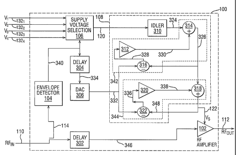
Referring to Fig. 1, there is illustrated an RF amplification stage 100 in
accordance with the general principles of the present invention. The RF
amplification
stage 100 includes an RF amplifier 102, a supply voltage selection block 106,
an
envelope detector 1'04, anda supply voltage-adjustment block 108.
The supply voltage selection block 106 receives four supply voltages V1-V4 on
respective input lines 1321-1324. The selected supply voltage is output from
the
supply voltage selection block 106 on line 120. The RF amplification stage 100
receives an RF input signal RFJN on line 110. The envelope detector 104 has an
input 114 coupled to line 110 to thereby detect the RF input signal. The
envelope
detector provides an output on line 118 to the supply voltage selection block
106 to
provide the necessary information for the supply voltage selection to take
place. In
addition, and in accordance with the present invention, the envelope detector
104
provides a second output on line 116 to the supply voltage adjustment block
108.
Supply voltage adjustment block 108 additionally receives the output of the
supply
voltage selection block on line 120. The supply voltage adjustment block 108
generates an adjusted supply voltage on line 122 for the RF amplifier 102. The
adjusted supply voltage on line 122 preferably forms a feedback input to the
supply
voltage adjustment block 108. As discussed hereinbelow a feedback arrangement
is
preferable in embodiments of the invention, although feedforward arrangements
may
also be used.
As discussed in further detail hereinbelow, the supply voltage adjustment
block 108 operates in accordance with the principles of the preferred
embodiment of
the present invention to adjust the supply voltage signal on line 122, in
dependence
upon the signal on line 116 and the feedback adjusted supply voltage on line
122, to
provide adjusted supply voltage Vs on line 122 to the RF power amplifier 102.
The
CA 02516706 2005-08-19
WO 2004/075398 PCT/GB2003/004507
8
RF power amplifier receives as its signal input the RF input signal on line
110. The
RF amplifier 102 provides on line 112 the RF output signal RFOUT.
The operation of the RF amplification stage 100 in accordance with the
present invention will be described further hereinbelow. However reference is
first
made to Fig. 2(a), which illustrates the concept of envelope tracking supply
voltage,
and the problems associated therewith. Referring to Fig. 2(a), there is
illustrated a
plot of voltage against time. On the voltage axis, there is illustrated four
specific
voltage levels VI-V4 corresponding to the voltage levels provided to the
supply
voltage selection block 106 of the RF amplification stage ofF1g: 1:-I1 should
be noted
that the provision of four voltage supplies is illustrative, and the RF
amplification
stage may in fact be provided with more or less voltage supplies in accordance
with
implementation requirements.
Curve 202 of Fig. 2(a) illustrates the voltage envelope of the RF input signal
to
the RF amplification stage, i.e. the signal on line 110. The dash line curve
206
illustrates the idealised voltage supply envelope for such an RF input signal.
As can
be seen, the dash line curve 206 tracks the RF input signal envelope 202 to
provide
an ideal power supply for the current input signal level. As such, the
idealised power
supply voltage avoids any wasted power and consequently is very efficient.
The stepped curve 204 illustrates a typical voltage supply to an RF power
amplifier based on a switch supply voltage of four levels, reflecting
performance
typical in prior art implementations. As the envelope 202 of the RF input
signal
reaches the voltage levels V1-V4, the supply voltage is appropriately
switched. As
can therefore be seen from Fig. 2(a), the supply voltage 204 steps between the
four
supply voltage levels. As such, the supply voltage level to the RF amplifier
is
frequently excessive. As illustrated by the hatched area 208, the stepped
supply
voltage implementation of the prior art is generally significantly less
efficient than the
idealised solution. The hatched area 208 in Fig. 2(a) represents wasted
energy,
corresponding to supply voltage levels above the idealised level and which is
consequently unnecessary. Referring to Fig. 2(b), there is illustrated the
efficiency improvement achieved in accordance with the present invention. The
stepped curve 205 illustrates the voltage supply generated by the switched
supply
CA 02516706 2005-08-19
WO 2004/075398 PCT/GB2003/004507
9
voltages. The supply voltage 205 provided by the supply voltage selection
block, as
discussed hereinbelow, tracks above and below the envelope 202. Such a
function is
provided, in the preferred embodiment, due the use of an AC amplifier in the
supply
voltage adjustment block 108. The embodiments of the present invention result
in an
actual supply voltage to the amplifier which more closely follows the
idealised supply
voltage 206, resulting in improved efficiency and a final voltage to the
amplifier which
is more closely aligned to the idealised voltage 206. As will be discussed
hereinbelow, in an embodiment the supply voltage selection block may provide
at its
output a step function equivalent to function 204 in Figure 2(aj. IN'such an
arrangement a DC offset is provided between at the output of the supply
voltage
selection block to provide a function equivalent to function 205 of Figure
2(a).
The RF amplification stage of Fig. 1, in accordance with the present invention
and embodiments described further hereinbelow, provides an improved solution
in
which the switched supply voltage more closely tracks the idealised supply
voltage
envelope, as shown in Fig. 2(b), and minimises wasted energy and thereby
maximises efficiency.
The RF amplification stage 100 in accordance with the present invention
comprises an RF amplifier 102 that may be connected to one of a number of
efficiently generated DC power supplies (V1-V4) through the supply voltage
selection
block 106 and the supply voltage adjustment block 108. The function of the
supply
voltage selection block 106 and supply voltage adjustment block 108 is to
approximately follow, as closely as possible, the envelope of the input signal
without
incurring additional energy dissipation, as represented by hatched area 208 in
Fig.
2(a).
In general, given a selection of the desired supply voltage for the RF input
signal to be amplified, the supply voltage selection block 106 connects the
selected
supply voltage to its output on line 120. The supply voltage adjustment block
108
functions to apply an appropriately adjusted version of the supply voltage on
line 120
to the RF amplifier 102 in such a way as to approximate envelope tracking at
the
amplifier supply, but without introducing the reduced bandwidth or reduced
efficiency
associated with linear devices providing the full range of RF amplifier supply
CA 02516706 2005-08-19
WO 2004/075398 PCT/GB2003/004507
voltages. This configuration allows the amplifier to achieve high efficiency
at high
modulation bandwidths.
Referring to Fig. 3, there is shown a preferred implementation of the RF
amplification stage 100 of Fig. 1 in accordance with the preferred embodiment
of the
5 present invention. Where elements of the RF amplification stage 100
correspond to
elements shown in Fig. I the same reference numeral is used.
As in Fig. 1, the RF amplification stage 100 includes the envelope detector
104, the supply voltage selection block 106, the RF amplifier 102, and the
supply
voltage adjustment block 108. In Fig. 1, the envelope detector 104 is
illustrated
10 providing two distinct outputs on lines 118 and 116. In the embodiment of
Fig. 3, the
envelope detector 104 provides a 'single output on line 340, which provides
the input
to the supply voltage selection block 106 and an input to a delay element 304.
The
output of delay element 304 on line 334 forms an input to a digital-to-
analogue
converter (DAC) 306, which provides an output on line 332 forming an input to
the
supply voltage adjustment block 108 equivalent to the signal on line 116 in
Fig. 1.
The RF amplifier 102 is further provided with a delay element 302 at its
input, such
that the RF input signal on line 110 forms an input to the delay element 302,
and the
output of the delay element on line 346 forms the input to the RF amplifier
102. Note
that in an actual implementation, delay 302 could alternatively be connected
in the
path between sample 114 and envelope detector 104 instead of before the RF
amplifier. The delay element is preferably placed in the path (supply or RF
amplifier)
that has the smallest delay.The supply voltage adjustment block 108 generally
includes an idler 310, a first feedback circuit 342 and a second feedback
circuit 344.
The idler 310 receives the output of the supply voltage selection block 106 on
line
120. The idler 310 provides an output on line 324 forming a first input to a
summer
314 of the first feedback circuit 342. The output of the summer 314 is
provided on
line 326, and forms the output of the first feedback circuit 342. The signal
on line 326
additionally forms a first input to a subtractor 316. The second input of the
subtractor
316 is provided by the output of the DAC 306 on line 332. The output of the
subtractor 316 is provided on line 328 and forms an input to an AC amplifier
312, the
output of which on line 330 forms the second input to the summer 314. The
second
CA 02516706 2005-08-19
WO 2004/075398 PCT/GB2003/004507
11
feedback circuit 344 is constructed similarly to the first feedback circuit
342. The
input to the second feedback circuit 344 is provided by the output of the
first
feedback circuit 342 on line 326, which forms a first input to a summer 318 of
the
second feedback circuit. The output of the summer 318 on line 348 forms a
first
input to a subtractor 322, the second input to which is formed by the output
of the
DAC 306 on line 332. The output of the subtractor 322 on line 336 forms an
input to
a HF amplifier 320, the output of which on line 338 forms the second input of
the
summer 318. The output of the summer 318 on line 348 also forms the supply
voltage input Vs on line 122 'to the RF amplifier 102.
In general, therefore, each feedback circuit receives an input voltage and
outputs an adjusted version of said voltage. The adjustment is performed in
dependence on the output of the feedback circuit (defining the feedback path)
and a
reference signal which in the described embodiment is formed by the output of
the
envelope detector 104.
The supply voltage adjustment block 108 operates to provided an adjusted
voltage level to the RF amplifier 102 which tracks the voltage level of the
envelope
representing the input to the RF amplifier, but which has a large output
current
corresponding to the large output current provided by the output of the supply
voltage
selection block 106.
The general principle of operation of the RF amplification stage 100 of Fig. 3
is
now described. The envelope detector 104 and supply voltage selection 106
provides a minimised loss predictive feed forward path that approximates the
required voltage supply tracking waveform. The envelope detector 104 provides
on
its output line 340 the detected envelope of the RF input signal on line 110,
which
information is provided to the voltage supply selection block 106.
The supply voltage selection block 106, which is preferably implemented as a
splicer network, is connected to a plurality, in the embodiment four, of fixed
high
efficiency DC power supplies. The splicer network is preferably a network of
transistors and diodes specifically designed to connect a selected supply
voltage to
the output on line 120 with a minimum of switching transients. The supply
voltage
selection 106 preferably operates on the output of the envelope detector 104
to
CA 02516706 2005-08-19
WO 2004/075398 PCT/GB2003/004507
12
switch between the voltage supplies at its input as the voltage level
indicated by the
envelope detector 104 of the RF input signal rises and falls above and below
threshold voltage levels corresponding to the respective supply voltages. In
this way,
the supply voltage selection block 106 provides on its output 120 an
appropriate one
of the supply voltages V1-V4.
The implementation of the supply voltage selection block to provide a voltage
function 205 as illustrated in Fig. 2(b) is within the scope of one skilled in
the art. In a
preferred implementation a DSP provides digital signals in a'thermometer code'
format (i.e. 0000, 0001, 0011,-0111, 1.111). The splicer network is preferably
an
arrangement of diodes and transistors that respond to this digitally coded
signal by
switching to the highest voltage level representing a level '1' logic signal.
All lower
level switches are turned off by means of the circuit function implemented
within the
splicer network, and without intervention from a DSP.
As discussed above, in an alternative arrangement the supply voltage
selections block 106 may output a function such as function 204 in Figure
2(a), and a
dc offset circuit may be provided at its output. The need to have a function
such as
function 205 in Figure 2(b) will become apparent in the following description.
The purpose of the delay block 304 at the input to the DAC 306 is described
further hereinbelow. Generally the delay block ensures the timing of signals
in the
amplification stage is synchronised.
The DAC 306 is provided on the basis that the RF input signal is a digital
signal. However, the present invention is not limited in its use to digital
applications.
The DAC 306 converts the envelope detector output on line 340 provided via the
delay element 304 into an analogue format for input on line 332 to the supply
voltage
adjustment block 108.
The idler 310, and the first and second feedback circuits 342 and 344, operate
on the selected supply voltage on line 120 to provide an improved and
efficient
voltage supply signal on line 122 to the RF amplifier.
The idler 310 provides interpolation of the signal at its input on line 120 to
generate an output on line 324. The idler 310 is preferably a circuit
consisting of
low-loss energy storage elements, and acts to redistribute energy supplied via
the
CA 02516706 2005-08-19
WO 2004/075398 PCT/GB2003/004507
13
splicer network of the supply voltage selection block 106 in an optimal
fashion to
improve amplifier efficiency and reduce unwanted emissions.
The first feedback circuit 342 is a corrective AC feedback circuit or
correction
circuit and functions to provide fine correction to the output of the
predictive
feedforward path on line 324. The AC feedback circuit 342 increases efficiency
The second feedback circuit is a low power high frequency corrective circuit
which removes any residual high frequency glitches from the output of the
first
feedback circuit.
It should be noted that although the preferred embodiment of Fig. 3
illustrates
two feedback circuits connected in a cascade arrangement, the invention is not
limited to such an arrangement. A single feedback circuit or any number
greater than
two may be provided may be provided. Where a single feedback circuit is
provided,
it is preferably an AC feedback circuit. It should also be noted that the
idler 310 is
not essential to the present invention, and is used in preferred embodiments.
Further, the supply voltage adjustment block may be implemented by using
feedforward circuit(s) in some or all of the corrective blocks in the cascade.
In general the supply voltage selection block 106 and the envelope detector
104, can be considered to form a minimal loss predictive feedforward path,
which
provides an approximation of the required tracking waveform for the supply
voltage to
the RF amplifier. When used, the output of the idler 310 forms the output of
the
feedforward path.
In general, in the preferred embodiment the supply voltage adjustment block
108
comprises a corrective feedback path. Of course, where provided, the idler 310
does
not form part of such path. The supply voltage adjustment block 108 may
comprise a
plurality of corrective feedback paths. Where a plurality of corrective
feedback paths
are provided, they are preferably provided in cascade.As discussed further
hereinbelow, in embodiments preferably clamping and DC restoration means are
provided in the supply voltage adjustment block 108 in order to overcome any
limitations of AC feedback and DC tracking.
The delay block 304 is preferably provided in order to remove any differential
time delay between the predictive and corrective parts of the RF amplification
stage
CA 02516706 2005-08-19
WO 2004/075398 PCT/GB2003/004507
14
100. The delay element 302 is inserted in the RF input signal path for the
purpose of
compensating for the delay of the amplification stage 100.
The operation of the supply voltage adjustment block 108 is now further
described. The DAC 306 effectively provides on line 332 a reference signal for
use
by the supply voltage adjustment block 108. The signal on line 332 represents
the
envelope of the RF input signal detected by the envelope detector 104, and
therefore
it represents a reference level for the supply voltage which should be
supplied to the
RF amplifier 102 at any instant in order to achieve maximum efficiency. This
envelope corresponds to the envelope 202 of Fig. 2(b) above.
The signal provided by the supply voltage selection block 106 on line 120
corresponds to the step function 205of Fig. 2(b) above. In accordance with the
preferred embodiment of the present invention the power supply voltage
selection
block rounds to the nearest supply voltage level, as shown in Figure 2(b),
whereas
the prior art always truncates upwards as shown by curve 204 in Fig. 2(a). The
purpose of the RF amplification stage 100 is to adapt the step function on
line 120 in
dependence upon the reference signal on line 332 in order to provide a signal
at the
supply voltage input to the RF amplifier which closely approximates the
idealised
supply voltage indicated by dash line 206 of Fig. 2(b).
As discussed above, the idler 310 is not essential to the implementation of
the
present invention. The idler is preferably a reactive LC (inductor-capacitor)
combination, provided on the output of the supply voltage selection block 106
in
order to improve efficiency. The addition of the idler, which can store energy
from
the supply voltage selection block and release it as required by the
amplifier,
improves the efficiency of the RF amplification stage in achieving a closer
match of
the amplifier's optimal power supply requirements. The idler circuit therefore
assists
in improving efficiency for rapidly changing waveforms and for reducing
unwanted
emissions.
The use of the idler is advantageous, in smoothing the output of the supply
voltage selection block. It should be noted, however, that forming a feedback
loop
from the output of the idler to the supply voltage selection block in attempt
to provide
correction equivalent to the supply voltage adjustment block 108 would not
provide a
CA 02516706 2005-08-19
WO 2004/075398 PCT/GB2003/004507
practical solution. Whilst the idler advantageously smoothes out output of the
supply
voltage selection block, as its name suggests it does so at the expense of
speed.
The idler is too slow to be incorporated in a corrective feedback loop, and a
practical
correction circuit could not be achieved in this way.
5 The provision of a feedback loop in the supply voltage adjustment block, in
accordance with the preferred embodiment of the invention, allows for a fast
corrective loop with a wide bandwidth. Similar advantages are obtained for the
feedforward case.
The AC corrective amplifier 312 of the first feedback circuit 342 requires an
10 AC signal at its input. This is achieved by the supply voltage selection
block rounding
to the nearest supply voltage level rather than truncated to the highest
level. such a
step function is necessary for the AC correction to work. As can be seen from
Figure
2(b), the input to the AC amplifier 312 is the difference between the supply
voltage
signal and the reference signal. This can only be an AC signal if the supply
voltage
15 signal alternates above and below the reference signal, thus producing a
usable
input for the amplifier 312.
The process of rounding the power supplies in the voltage selection block 106,
rather than truncating them as in the prior art, is eqivalent to doubling the
effective
number of power supplies compared to a prior art system.
This doubling is effectively achieved by halving the error relative to the
prior
art. So for the same number of power supplies provided, with the invention the
error
is halved such that there are in effect twice as many power supplies as in the
prior
art. Alternatively, the invention may be considered to offer the same error as
a prior
art system with only half the number of supplies needed.
The subtractor 316 of the first feedback circuit receives, in effect, the
current
output of the supply voltage selection block 106, and the envelope reference
signal
on line 332. The output of the subtractor 316 on line 328 is thus the
difference
between the two signals, representing the error in the signal at the output of
the
supply voltage selection block compared to the ideal voltage supply 332. The
amplified error signal on line 330 is then added to the output of the supply
voltage
selection block 106, in order to provide a supply voltage signal on line 326
which is
CA 02516706 2005-08-19
WO 2004/075398 PCT/GB2003/004507
16
compensated for the error. The AC amplifier 312 has to handle error signals
with a
high peak to mean ratio, and is thus preferably implemented as a class G
amplifier
with multiple switch supplies for optimum efficiencies. The amplifier 312
handles
much lower power levels than the supply voltage selection block 106, and
therefore
can be implemented with smaller, faster devices.
The second feedback circuit 344 provides for additional correction
means. Further correction means may be added as required, and furthermore only
one correction means may be required. The corrective circuits of the supply
voltage
adjustment block 108 effectively force the supply voltage of the RF amplifier
to
closely track the reference provided by the envelope detector 104 over a wide
range
of frequencies.
The summation means 314 and 318 may preferably be implemented as
transformers.
The supply voltage selection block 106, preferably comprising a splicer
including a switch matrix, is preferably controlled by a digital signalling
processing
means, which digital signalling processing means may further include the delay
elements 302 and 304, the DAC 306 and the envelope detector 104. The specific
implementation of such digital signalling processing means, including the
various
associated elements, will be within the scope of a person skilled in the art.
Implementing the AC amplifier 312 of the first feedback circuit 342 with a
plurality of switched voltage supplies advantageously means that the number of
supply voltages to the RF amplifier 102 may be significantly increased. For
example,
if the AC amplifier 312 was associated with m supply voltages, and the main
supply
voltage selection is associated with n supply voltages, the total number of
supply
voltages available to the RF amplifier 102 is m*n. As discussed above, the use
of
power supply rounding in the supply voltage selection block effectively
doubles the
number of power supplies, such that the total number of power supplied may
become
2*m*n.
Such an embodiment of the present invention offers significant advantages.
As discussed above, the small size of the amplifier 312 means that it is not
associated with the problems associated with the supply voltage selection
block 106,
CA 02516706 2005-08-19
WO 2004/075398 PCT/GB2003/004507
17
which problems the invention is intended to overcome. The envelope tracking
feedback loop of the supply voltage adjustment block 108 does not require any
large
geometry devices, or the high current large geometry devices being providing
at the
predictive feedforward path rather than the feedback loop. As such, there is
provided
a large increase in the power bandwidth of the envelope tracking loop.
Referring to Fig. 4, there is illustrated the adaptation of the amplifier 312
in
order to provide a variable supply voltage to said amplifier. The provision of
such
variable supply to the amplifier may be in accordance with techniques known in
the
art. As shown in Fig. 4, there is provided a voltage selector 402, which
receives an
input of a line 408 coupled to the signal input of the amplifier. The input on
line 408
represents the amplitude of the input signal. The voltage selector 402 also
receives
a plurality of supply voltages, e.g. two supply voltages Vx and Vy on lines
406 and
404. The voltage selector 402 selects one of the supply voltages for output on
line
410 as the supply voltage for the amplifier. The supply voltage Vx and Vy is
selected
in dependence on the envelope on line 408.
The implementation of the amplifier 312 with selectable power supplies is not
limited to such an arrangement. The implementation may be achieved, for
example,
under the control of a DSP.
As discussed further hereinbelow, in a preferred embodiment the use of
clamping and restoration means removes the need for any DC corrective
feedback.
Further discussion of detailed, preferable aspects of implementations of the
present invention are discussed hereinbelow. Firstly, the implementation of an
embodiment of the present invention utilising a feedforward corrective circuit
is
discussed.
In the embodiments of Figs. I and 3, the corrective circuit or corrective path
in
the supply voltage adjustment block is implemented as a feedback arrangement.
The general principle of such an arrangement is shown in Fig. 5(a). Generally
an
approximate function block 556 generates a signal to be corrected, and a
reference
function block 554 generates a reference signal. The signal to be corrected
forms a
first input to a summer 552, the output of which on line 558 represents the
corrected
signal. The reference signal and the corrected signal form inputs to an
amplifier 550,
CA 02516706 2010-01-29
18
the output of which forms a second input to the summer 552. It should be noted
that this is
the general principle of the feedback paths of Fig. 3, the input to the
amplifier 312 being
provided by a subtractor which receives the corrected output and the reference
signal as inputs.
Referring to Fig. 5(b), there is illustrated the principle, in an alternative
embodiment, of a
feedforward arrangement. The signal to be corrected again forms a first input
to the summer
562. An amplifier 560 receives as inputs the signal to be corrected and the
reference signal.
The amplifier output forms the second input to the summer 562, the output of
which again
forms the corrected output 564. A feedforward arrangement as shown in Fig.
5(b) may be used
in the embodiments of Figs. 1 and 3 in place of a feedback arrangement.
As the splicer network of the supply voltage selection block is implemented as
part of
a predictive feedforward controller, adaptive control of the splicer
parameters improves
efficiency. A local version of the splicer output is therefore preferably
generated digitally from
models of the elements in the splicer network. The decision to change the
splicer level, i.e.
the output supply voltage, is made in order to minimise the difference between
the locally
generated splicer waveform (including consideration of past, present and
future values) and the
envelope representation.
Included in this model are:
a) switch delay and risetime parameters;
b) filter parameters; and
c) slicer voltages and FET resistances.
The locally generated parameters are related to the actual parameters by
comparing
locally generated measured parameters with those obtained from the actual
circuit. The actual
parameters that are most convenient to measure is the signal error from
comparison of the
splicer output and the averaged current consumption of the AC error amplifier
312 of the first
feedback circuit 342. An optimisation algorithm may be provided which aims to
minimise the
current consumption of the AC amplifier 312 by adjustment of the above
measured parameters
in the model. Convergence of the optimisation will be assisted by
consideration of the signed
error or the splicer network to provide localised error
CA 02516706 2005-08-19
WO 2004/075398 PCT/GB2003/004507
19
correction. Selection of the supply to which the amplifier will be connected
is made
by a supply selection circuit.
The splicer circuit of the supply voltage selection block 106 consists of a
network of switching transistors that are switched by logic signals
originating in the
digital signal processing (DSP) means. The implementation of such adaptive
control
will be understood by one skilled in the art.
Referring to Fig. 6, there is illustrated the implementation of DC clamping
and
dc offset restoration in accordance with a preferred embodiment of the
invention. DC
clamping is provided to prevent accumulation of a DC error signal. DC offset
restoration compensates for any adjustment in the actual supply voltage level.
For
example, although the selected supply voltage is 7V, it may actually be only
6.5V due
to circuit degradations. DC offset restoration and DC clamping may be provided
together, as described in this embodiment, or separately.
As before, elements in Fig. 6 corresponding to elements in earlier figures are
identified by the same reference numerals. Fig. 6 illustrates only a portion
of the RF
amplification stage 100. Fig. 6 illustrates the supply voltage selection block
106, and
the first feedback circuit or correction circuit 342 as illustrated in Fig. 3.
Also shown
is the DAC 306 of Fig. 3. In Fig. 6, the DAC 306 is shown to receive an input
on lines
504 from a DSP 500. The DSP 500 also provides control inputs on lines 502 to
the
supply voltage selection block 106. As discussed hereinabove, in such an
embodiment the DSP 500 may be considered to include the envelope detector 104
and delay element 304 of Fig. 3. As further shown in Fig. 6, the output of the
first
feedback circuit or correction circuit 342 on line 326 is provided to either a
further
cascaded feedback/correction circuit or directly to the supply voltage of the
RF
amplifier. In order to accommodate DC clamping, the RF amplification stage is
further modified to include a subtractor 512, which receives as a first input
the output
on line 120 of the first feedback/correction circuit, and as a second input
the
reference signal on line 332 from the DAC 306. The output of the subtractor
512 is
provided on line 510 to a single bit analogue-to-digital converter 508, which
provides
an output on line 506 to the DSP 500. The DSP 500 receives as an input the
output
CA 02516706 2005-08-19
WO 2004/075398 PCT/GB2003/004507
of the subtractor 316, representing the error signal in the supply voltage
signal. In
addition the DSP 500 generates an output on line 518 which forms an input to a
VDD
clamp circuit 514. The output of the clamp circuit 514 on line 516 controls a
clamp
means, generally designated by reference numeral 520, connected to the output
330
5 of the AC amplifier 312.
Referring to Figure 7, it can be understood that the envelope signal goes
below the lowest supply voltage level at certain points. For example, if it is
assumed
for the sake of example that line 804c represents a lowest supply voltage,
between
points 803 and 805 the envelope goes beneath the lowest supply voltage. During
10 such time interval, there is no need for the supply voltage to the
amplifier to be
tracked by the correction circuit. The embodiments of the present invention
therefore
detect this condition, and use the existence of the condition to apply dc
restoration as
discussed further hereinbelow.
The subtractor 512 subtracts the reference signal on line 332 from the current
15 supply voltage on line 120, and provides the difference to the I bit
analogue to digital
converter 508. The most significant bit identifies whether the current
envelope level is
above or below the lowest supply voltage,fine control of envelope clamp off
level
being achieved by integration over time..
Responsive to the DSP detecting the appropriate condition, a command signal
20 is sent to the Vdd clamp circuit on line 518, which in turn controls the
clamp means
50 to turn on. When turned on the clamp means 520 pulls the output of the ac
amplifier on line 330 to a known reference level, preferably ground. The clamp
means 520 is preferably a transistor.
The purpose of the DC clamping is to reset the amplifier 312 to a known state
in order to avoid the build-up, over time, of a DC error. This is achieved as
described
above in a preferred embodiment. However other techniques may be provided for
dc
clamping. For example, The dc may be fed back, for example, by slow adjustment
of
the plurality of power supplies to the selection block 106 or use of a series
pass
transistor. Thus a certain time period is allocated as the DC clamping
interval.
This comparison is necessary to allow for voltage drops in any components
and conductors connected between the current supply voltage and the lower
supply
CA 02516706 2005-08-19
WO 2004/075398 PCT/GB2003/004507
21
voltage during the clamp periodln any practical implementation, there will
always be
some uncertainty between the actual lower supply voltage level when delivering
current to the RF amplifier and the level initially assumed by the clamped
level at the
envelope detector. The comparator 512 corrects for this and ensures that the
envelope detector is clamped off at a level equal to the actual lower supply
voltage.
The signal on line 506 is preferably gated in an integrator in the DSP 500.
The
output of the integrator sets the clamp level of the amplitude reference
digital output
on line 518. The effect is to alter the clamp level of the reference DAC 306.
The
integration thus compensates for variations in the supply voltage such fihat
clamp-ofl=
occurs at the actual supply voltage (e.g. 6.5V) rather than the theoretical
supply
voltage (e.g. 7V). The integrator thus adjusts the clamping such that the
clamp off
voltage is equal to the value of the lowest supply input to 106 minus any
additional
voltage drops in 106.
During the clamping period, the value of the AC feedback output is set to zero
by switches 520 that are turned on during the clamping period. This DC
restoration
enables an amplifier to be used with a finite lower cut-off frequency.
The error waveform has a flat frequency spectrum, which implies that the use
of a bandpass AC amplifier, such as amplifier 312, may result in significant
residual
error due to the inability of the amplifier to follow low frequency
components. By
clamping the AC output during the clamping interval, and provided the low
frequency
time constant of the amplifier 312 is more than the interval between clamps,
accurate
tracking can be assured.
Referring to Fig. 7, the advantage achieved in the preferred embodiment
utilising DC clamping is illustrated. The curve 802 of Fig. 7 represents the
envelope
of the RF input signal. The straight lines 804a-804b illustrate the adjustment
of the
clamped DAC levels, i.e. the effect of dc removal.
Another significant source of low frequency error is any mismatch between the
expected splicing voltages in the DSP 500 and the voltages existing at the
output of
the supply voltage selection block 106. This is equivalent to an error in the
slicing
threshold. A splicer adaptation algorithm, as described above, removes such
errors
in the thresholding.
CA 02516706 2010-01-29
22
Another DSP adjustment which may be preferably implemented is to delay the DAC
envelope reference waveform output relative to the output of the supply
voltage selection block
106, as represented by delay element 304 in Fig. 3 and discussed hereinabove.
An example delay balancing implementation is illustrated in Fig. 8, which
includes the
modifications introduced in Fig. 6 to provide for a clamping of a DC level in
the
feedback/correction circuit. The provision of the delay balancing
implementation is preferable
so as to effect maximum efficiency, since the AC amplifier 312 output is then
minimised. An
appropriate modification to the preferred embodiment of Fig. 6 is shown in the
further
preferred embodiment of Fig. 8. Only those elements necessary to understand
this embodiment
of the invention are illustrated.
Referring to Fig. 8, the digital signal processor 500 includes, in this
preferred
embodiment, an interpolator 602, a time differentiator 604, a multiplier 608,
a summer 606,
a splice control block 610, and an envelope level source 612. As will be
understood, the
envelope level source 612 represents the generation of the reference envelope,
the preferable
generation of which has been described hereinabove with reference to Figs. 1
and 3.
In accordance with this embodiment of the invention, the elements of the DSP
500
shown in Fig. 8 function to provide delay balancing.
The envelope reference waveform generated by the envelope level block 612 on
line
614 is provided to the interpolator 602, which provides an output on line 616
to the time
differentiator 604. The output on line 616 also forms the input to the DAC 306
on line 334.
The output of the time differentiator 604 on line 622 comprises the time
derivative of the
envelope reference waveform.
The time derivative of the envelope reference waveform on line 622 is
multiplied in
multiplier 608 with the single bit error signal on line 506 from the one-bit
ADC 508. The
multiplied result is presented on line 620 at the output of the multiplier
608.
The multiplied result on line 620 forms a first input to the summer 606, which
is
configured to function as an integrator. The output of the summer 606 on line
618
CA 02516706 2005-08-19
WO 2004/075398 PCT/GB2003/004507
23
is fed back to form a second input to the summer. The integrated output on
line 618
is provided as an input to the interpolator 602 to control or steer the delay
of the
reference waveform.
Sub-sample interval delay resolution can be achieved by interpolation of the
reference waveform in the interpolator 602.
In summary, Figure 8 shows a preferred implementation of the delay element
304 of Figure 3, including the dc clamping control of Figure 6. Other possible
implementations of the delay element 304 will be within the scope of one
skilled in
the art.
The embodiments described hereinabove allow the RF amplification stage to
operate without external adjustment for the majority of multi-carrier cases
within
power and bandwidth constraints. However there are two specific cases which
may
require the DSP 500 of Figure 8 to automatically modify its operating mode.
Some
modification would be required to enable the envelope tracking to be accurate
for
constant envelope or slowly varying signals. An example of such a signal is
GPRS
(general packet radio services) in which only one carrier or two closely
spaced
carriers are required to be amplified. In such a scenario, the interval
between
successive clamps could be very long. This would require the DSP to evoke a
time-
out at which point second order delta sigma pulse width modulation between the
nearest supplies is carried out by the splice control module 610. The use of
pulse
width modulation is acceptable in such a scenario because there is minimal
high
frequency envelope power present.
A further scenario arises when two carriers of an equal amplitude are present
but separated by a large frequency interval, but the envelope depth is not
sufficient to
reach the minimum supply clamp. In this case, the clamping level is moved to
the
next highest supply level, and all other functions remain as in the multi-
carrier case.
Finally, referring to Fig. 9, there is illustrated the efficiency improvement
provided in accordance with the present invention. Fig. 9 illustrates a plot
of power
amplifier efficiency against power amplifier supply voltage. As can be seen,
the thick
line 704 represents the supply voltage switching in accordance with the
present
CA 02516706 2005-08-19
WO 2004/075398 PCT/GB2003/004507
24
invention, whereas the thin line 702 represents the range in power supply
voltage
achieved in the prior art.
Curve 706 of Figure 9 illustrates the significant advantage which can be
achieved when multiple supply voltages are used including the implementation
of
amplifier 312 as a Class G amplifier. As more supply voltages are provided,
then the
drop in efficiency between supply voltage levels is more of a ripple than the
sawtooth' waveform 704 achieved with a small number of power supplies.
The RF amplifier 102 preferably drives an RF load such as an antenna.
The present invention has been described herein by way of reference to
particular preferred embodiments. However the invention is not limited to such
embodiments. The present invention has p1 articular application in relation to
RF
amplifiers, but is not limited to such implementation. The invention can be
advantageously utilised in any environment where switched, selectable voltage
supplies are provided.
The described preferred embodiments utilising an RF amplifier are not limited
to any particular load being driven by such RF amplifier. However it is
envisaged that
such an RF amplifier will typically drive an antenna. As such, the present
invention
has particularly advantageous uses in the field of communications, including
the field
of mobile communications.