Note: Descriptions are shown in the official language in which they were submitted.
CA 02516915 2005-08-23
Internal reference: IRDM.019 NON-EP / IDC-0040
DISPLAY REGION ARCHITECTURES
Back.-r
Field of the Invention
The field of the invention relates generally to microelectromechanical systems
(MEMS),
and more particularly to architectures of display regions having arrays of
MEMS elements.
Description of the Related Technology
The aperture of a pixel, or any other display region, is the area of the pixel
that outputs
light. In general, the aperture of a pixel is reduced by row and column cuts
that are used to
electrically isolate rows and columns of sub-pixels, or sub-regions. These row
and column cuts
do not generally output light, so the cuts correspond to "dead areas" on the
pixel. Accordingly,
as the number of sub-regions in a pixel increases, the dead areas of the pixel
also increase,
thereby decreasing the aperture of the pixel. Thus, by dividing a pixel into
sub-pixels to increase
the resolution of the pixel, the aperture of the pixel is reduced due to these
dead areas.
Accordingly, improved systems and methods for increasing a resolution of a
pixel with a reduced
effect on the aperture of the pixel are desired.
As the number of leads connecting a pixel to the device driver increases
(e.g., due to
dividing the pixel into separately actuatable sub-pixels), the complexity of
routing the leads also
increases. In addition, as the number of leads routed to a pixel increases,
the complexity of
attaching the driver to the display increases, and additional drivers that
handle additional leads
may also be necessary. Thus, as the number of leads increases, the complexity
and cost of
interconnecting the leads to the pixel also increase. Accordingly, when
designing a pixel, there is
typically a tradeoff between the available bit depth and the cost, complexity,
and aperture of the
pixel.
Summary of Certain Embodiments
The system, method, and devices of the invention each have several aspects, no
single
one of which is solely responsible for its desirable attributes. Without
limiting the scope of this
invention, its more prominent features will now be discussed briefly. After
considering this
discussion, and particularly after reading the section entitled "Detailed
Description of Certain
Embodiments" one will understand how the features of this invention provide
advantages over
other display devices.
In certain embodiments, a pixel having a bit depth per color comprises a
plurality of
substantially equally sized sub-regions having a first group of sub-regions
and a second group of
-1-
CA 02516915 2005-08-23
sub-regions. Each of the sub-regions of the first group includes a first
number of display
elements per color and each of the sub-regions of the second group includes a
second number of
display elements per color. The second number minus the first number is
substantially equal to
two raised to a power that is less than the bit depth per color.
In certain embodiments, a pixel having a bit depth comprises a plurality of
substantially
equally sized display elements each having an "on" position and an "ofi?'
position. The display
elements each emit visible light when in the "on" position. The plurality of
substantially equally
sized display elements includes a first group of display elements and a second
group of display
elements. The display elements of the first group each have an intensity of a
predetermined value
when in the "on" position and the display elements of the second group each
have an intensity of
a fraction of the predetermined value when in the "on" position. An intensity
of the pixel is equal
to an intensity of each of the plurality of display elements in the "on"
position.
In certain embodiments, a pixel having a bit depth n per color comprises a
first number N
of sub-regions, each sub-region having c display elements per color. Each
display element has a
first area. The pixel further comprises a second number M of sub-regions, each
sub-region
having c+2~°~P~ display elements per color. Each of (c-1) of the
c+2~°-P~ display elements has a
second area and each of 1+2~°-P~ of the c+2~°-P~ display
elements has a third area. The first area
and the second area are substantially equal and the third area is
substantially equal to the first
area divided by 1+2~°-P~, wherein p is less than n.
In certain embodiments, a method of arranging a plurality of display elements
in a pixel
comprises dividing the pixel into a first group of sub-regions and a second
group of sub-regions.
The sub-regions in the first and second groups have substantially equal areas.
The method
further comprises allocating a first number of display elements per color to
each of the sub-
regions of the first group. The method further comprises allocating a second
number of display
elements per color to each of the sub-regions of the second group. The second
number minus the
first number is substantially equal to two raised to a power that is less than
a bit depth per color
of the pixel.
1n certain embodiments, a display device responsive to signals having a
plurality of bits
comprises a plurality of pixels, each of the pixels comprising a plurality of
sub-regions. The
display device further comprises a first plurality of sub-regions, each sub-
region having a first
area. The first plurality of sub-regions is responsive to a first portion of
the plurality of bits. The
display device further comprises a second plurality of sub-regions, each sub-
region having a
second area. The second area is less than the first area. The second plurality
of sub-regions is
responsive to a second portion of the plurality of bits, wherein the bits of
the second portion are
less significant than the bits of the first portion.
-2-
CA 02516915 2005-08-23
In certain embodiments, a display device is provided, the display device
comprising at
least one pixel having a bit depth per color. The device further comprises
means for displaying
an image comprising a plurality of substantially equal sub-regions. The
displaying means
comprises means for displaying a first group of sub-regions, and means for
displaying a second
group of sub-regions, wherein the sub-regions of the first group and the
second group are
substantially equally sized, each of the sub-regions of the first group
including a first number of
display elements per color and each of the sub-regions of the second group
includes a second
number of display elements per color, wherein the second number minus the
first number is
substantially equal to two raised to a power that is less than the bit depth
per color.
In certain embodiments, a display device responsive to at least one signal
having a
plurality of bits is provided, the display device comprising means for
displaying an image
comprising a plurality of sub-regions. The displaying means comprises means
for responding to
a first portion of the plurality of bits, said responding means to the first
portion comprising a first
plurality of sub-regions, each sub-region of the first plurality of sub-
regions having a first area.
The displaying means further comprises means for responding to a second
portion of the plurality
of bits, said responding means to the second portion comprising a second
plurality of sub-regions,
each sub-region of the second plurality of sub-regions having a second area,
wherein the second
area is less than the first area, and wherein the bits of the second portion
are less significant than
the bits of the first portion.
In certain embodiment, a display device is provided, the display device
comprising at
least one pixel having a bit depth per color. The display device further
comprises means for
providing a first range of intensities, and means for providing a second range
of intensities.
BRIEF DESCRIPTION OF THE DRAWINGS
Figure 1 is an isometric view depicting a portion of one embodiment of an
interferometric modulator display in which a movable reflective layer of a
first interferometric
modulator is in a released position and a movable reflective layer of a second
interferometric
modulator is in an actuated position.
Figure 2 is a system block diagram illustrating one embodiment of an
electronic device
incorporating a 3x3 interferometric modulator display.
Figure 3 is a diagram of movable mirror position versus applied voltage for
one
exemplary embodiment of an interferometric modulator of Figure 1.
Figure 4 is an illustration of a set of row and column voltages that may be
used to drive
an interferometric modulator display.
Figure SA illustrates one exemplary frame of display data in the 3x3
interferometric
modulator display of Figure 2.
-3-
CA 02516915 2005-08-23
Figure SB illustrates one exemplary timing diagram for row and column signals
that may
be used to write the frame of Figure SA.
Figure 6A is a cross section of the device of Figure 1.
Figure 6B is a cross section of an alternative embodiment of an
interferometric
modulator.
Figure 6C is a cross section of another alternative embodiment of an
interferometric
modulator.
Figure 7 is a diagram schematically illustrating one embodiment of a pixel
including
multiple sub-regions.
Figure 8 is a diagram schematically illustrating an exemplary sub-region of
Figure 7, the
sub-region having a staggered RGB structure.
Figure 9 is a diagram schematically illustrating another exemplary sub-region
of Figure
7, the sub-region having a striped RGB structure.
Figure 10 is a diagram schematically illustrating another embodiment of a
pixel
comprising an 18 x 18 array of sub-regions.
Figure 11A is a close-up view schematically depicting one embodiment of one
sub-region
of the pixel illustrated in Figure 10.
Figure 11B is a close-up view schematically depicting one embodiment of one
further
subdivided sub-region of the pixel illustrated in Figure 10.
Figure 12 schematically illustrates another embodiment of a sub-region
structure of a
pixel having a reduced number of leads.
Figures 13A and 13B are system block diagrams illustrating an embodiment of a
visual
display device comprising a plurality of interferometric modulators.
DETAILED DESCRIPTION OF CERTAIN EMBODIMENTS
A bit depth of a pixel comprising multiple display elements, such as
interferometric
modulators, may be increased through the use of display elements having
different intensities,
while the lead count is minimally increased. An exemplary pixel with a single
display element
having an intensity of 0.5 and N display elements each having an intensity of
one can provide
about 2N + 1 shades (e.g., 0, 0.5, 1.0, 1.5, 2.0, [N + .5]). In comparison, a
pixel having N display
elements, each having an intensity of one, can only provide about N+1 shades
(e.g., 0, l, 2, ..., N).
Thus, using at least one display element having an intensity lower than the
intensity of each of
the other display elements increases the number of shades provided by the
pixel by an
approximate factor of two and increases the bit depth of the pixel, while
minimizing the number
of additional leads.
-4-
CA 02516915 2005-08-23
The following detailed description is directed to certain specific embodiments
of the
invention. However, the invention can be embodied in a multitude of different
ways. In this
description, reference is made to the drawings wherein like parts are
designated with like
numerals throughout. As will be apparent from the following description, the
invention may be
implemented in any device that is configured to display an image, whether in
motion (e.g., video)
or stationary (e.g., still image), and whether textual or pictorial. More
particularly, it is
contemplated that the invention may be implemented in or associated with a
variety of electronic
devices such as, but not limited to, mobile telephones, wireless devices,
personal data assistants
(PDAs), hand-held or portable computers, GPS receivers/navigators, cameras,
MP3 players,
camcorders, game consoles, wrist watches, clocks, calculators, television
monitors, flat panel
displays, computer monitors, auto displays (e.g., odometer display, etc.),
cockpit controls and/or
displays, display of camera views (e.g., display of a rear view camera in a
vehicle), electronic
photographs, electronic billboards or signs, projectors, architectural
structures, packaging, and
aesthetic structures (e.g., display of images on a piece of jewelry). MEMS
devices of similar
structure to those described herein can also be used in non-display
applications such as in
electronic switching devices.
One interferometric modulator display embodiment comprising an interferometric
MEMS display element is illustrated in Figure 1. In these devices, the pixels
are in either a
bright or dark state. In the bright ("on" or "open") state, the display
element reflects a large
portion of incident visible light to a user. When in the dark ("off' or
"closed") state, the display
element reflects little incident visible light to the user. Depending on the
embodiment, the light
reflectance properties of the "on" and "off ' states may be reversed. MEMS
pixels can be
configured to reflect predominantly at selected colors, allowing for a color
display in addition to
black and white.
Figure 1 is an isometric view depicting two adjacent pixels in a series of
pixels of a
visual display, wherein each pixel comprises a MEMS interferometric modulator.
In some
embodiments, an interferometric modulator display comprises a row/column array
of these
interferometric modulators. Each interferometric modulator includes a pair of
reflective layers
positioned at a variable and controllable distance from each other to form a
resonant optical
cavity with at least one variable dimension. In one embodiment, one of the
reflective layers may
be moved between two positions. In the first position, referred to herein as
the released state, the
movable layer is positioned at a relatively large distance from a fixed
partially reflective layer. In
the second position, the movable layer is positioned more closely adjacent to
the partially
reflective layer. Incident light that reflects from the two layers interferes
constructively or
destructively depending on the position of the movable reflective layer,
producing either an
overall reflective or non-reflective state for each pixel.
-5-
CA 02516915 2005-08-23
The depicted portion of the pixel array in Figure 1 includes two adjacent
interferometric
modulators 12a and 12b. In the interferometric modulator 12a on the left, a
movable and highly
reflective layer 14a is illustrated in a released position at a predetermined
distance from a fixed
partially reflective layer 16a. In the interferometric modulator 12b on the
right, the movable
highly reflective layer 14b is illustrated in an actuated position adjacent to
the fixed partially
reflective layer 16b.
The fixed layers 16a, 16b are electrically conductive, partially transparent
and partially
reflective, and may be fabricated, for example, by depositing one or more
layers each of
chromium and indium-tin-oxide onto a transparent substrate 20. The layers are
patterned into
parallel strips, and may form row electrodes in a display device as described
further below. The
movable layers 14a, 14b may be formed as a series of parallel strips of a
deposited metal layer or
layers (orthogonal to the row electrodes 16a, 16b) deposited on top of posts
18 and an intervening
sacrificial material deposited between the posts 18. When the sacrificial
material is etched away,
the deformable metal layers are separated from the fixed metal layers by a
defined air gap 19. A
highly conductive and reflective material such as aluminum may be used for the
deformable
layers, and these strips may form column electrodes in a display device.
With no applied voltage, the cavity 19 remains between the layers 14a, 16a and
the
deformable layer is in a mechanically relaxed state as illustrated by the
pixel 12a in Figure 1.
However, when a potential difference is applied to a selected row and column,
the capacitor
formed at the intersection of the row and column electrodes at the
corresponding pixel becomes
charged, and electrostatic forces pull the electrodes together. If the voltage
is high enough, the
movable layer is deformed and is forced against the fixed layer (a dielectric
material which is not
illustrated in this Figure may be deposited on the fixed layer to prevent
shorting and control the
separation distance) as illustrated by the pixel 12b on the right in Figure 1.
The behavior is the
same regardless of the polarity of the applied potential difference. In this
way, row/column
actuation that can control the reflective vs. non-reflective pixel states is
analogous in many ways
to that used in conventional LCD and other display technologies.
Figures 2 through 5 illustrate one exemplary process and system for using an
array of
interferometric modulators in a display application. Figure 2 is a system
block diagram
illustrating one embodiment of an electronic device that may incorporate
aspects of the invention.
In the exemplary embodiment, the electronic device includes a processor 21
which may be any
general purpose single- or multi-chip microprocessor such as an ARM, Pentium ,
Pentium II~,
Pentium III~, Pentium IV~, Pentium~ Pro, an 8051, a MIPS~, a Power PC~, an
ALPHA~, or any
special purpose microprocessor such as a digital signal processor,
microcontroller, or a
programmable gate array. As is conventional in the art, the processor 21 may
be configured to
execute one or more software modules. In addition to executing an operating
system, the
-6-
CA 02516915 2005-08-23
processor may be configured to execute one or more software applications,
including a web
browser, a telephone application, an email program, or any other software
application.
In one embodiment, the processor 21 is also configured to communicate with an
array
controller 22. In one embodiment, the array controller 22 includes a row
driver circuit 24 and a
column driver circuit 26 that provide signals to a pixel array 30. The cross
section of the array
illustrated in Figure 1 is shown by the lines I-1 in Figure 2. For MEMS
interferometric
modulators, the row/column actuation protocol may take advantage of a
hysteresis property of
these devices illustrated in Figure 3. It may require, for example, a 10 volt
potential difference to
cause a movable layer to deform from the released state to the actuated state.
However, when the
voltage is reduced from that value, the movable layer maintains its state as
the voltage drops back
below 10 volts. In the exemplary embodiment of Figure 3, the movable layer
does not release
completely until the voltage drops below 2 volts. There is thus a range of
voltage, about 3 to 7 V
in the example illustrated in Figure 3, where there exists a window of applied
voltage within
which the device is stable in either the released or actuated state. This is
referred to herein as the
"hysteresis window" or "stability window." For a display array having the
hysteresis
characteristics of Figure 3, the row/column actuation protocol can be designed
such that during
row strobing, pixels in the strobed row that are to be actuated are exposed to
a voltage difference
of about 10 volts, and pixels that are to be released are exposed to a voltage
difference of close to
zero volts. After the strobe, the pixels are exposed to a steady state voltage
difference of about 5
volts such that they remain in whatever state the row strobe put them in.
After being written,
each pixel sees a potential difference within the "stability window" of 3-7
volts in this example.
This feature makes the pixel design illustrated in Figure 1 stable under the
same applied voltage
conditions in either an actuated or released pre-existing state. Since each
pixel of the
interferometric modulator, whether in the actuated or released state, is
essentially a capacitor
formed by the fixed and moving reflective layers, this stable state can be
held at a voltage within
the hysteresis window with almost no power dissipation. Essentially no current
flows into the
pixel if the applied potential is fixed.
In typical applications, a display frame may be created by asserting the set
of column
electrodes in accordance with the desired set of actuated pixels in the first
row. A row pulse is
then applied to the row 1 electrode, actuating the pixels corresponding to the
asserted column
lines. The asserted set of column electrodes is then changed to correspond to
the desired set of
actuated pixels in the second row. A pulse is then applied to the row 2
electrode, actuating the
appropriate pixels in row 2 in accordance with the asserted column electrodes.
The row I pixels
are unaffected by the row 2 pulse, and remain in the state they were set to
during the row 1 pulse.
This may be repeated for the entire series of rows in a sequential fashion to
produce the frame.
Generally, the frames are refreshed and/or updated with new display data by
continually
CA 02516915 2005-08-23
repeating this process at some desired number of frames per second. A wide
variety of protocols
for driving row and column electrodes of pixel arrays to produce display
frames are also well
known and may be used in conjunction with the present invention.
Figures 4 and 5 illustrate one possible actuation protocol for creating a
display frame on
the 3x3 array of Figure 2. Figure 4 illustrates a possible set of column and
row voltage levels that
may be used for pixels exhibiting the hysteresis curves of Figure 3. In the
Figure 4 embodiment,
actuating a pixel involves setting the appropriate column to -Vb;as, and the
appropriate row to
+pV, which may correspond to -5 volts and +5 volts respectively Releasing the
pixel is
accomplished by setting the appropriate column t0 +Vb;as, and the appropriate
row to the same
+0V, producing a zero volt potential difference across the pixel. In those
rows where the row
voltage is held at zero volts, the pixels are stable in whatever state they
were originally in,
regardless of whether the column is at +Vb;$S, or -Vb;as~
Figure SB is a timing diagram showing a series of row and column signals
applied to the
3x3 array of Figure 2 which will result in the display arrangement illustrated
in Figure SA, where
actuated pixels are non-reflective. Prior to writing the frame illustrated in
Figure SA, the pixels
can be in any state, and in this example, all the rows are at 0 volts, and all
the columns are at +5
volts. With these applied voltages, all pixels are stable in their existing
actuated or released
states.
In the Figure SA frame, pixels (1,1), (1,2), (2,2), (3,2) and (3,3) are
actuated. To
accomplish this, during a "line time" for row 1, columns 1 and 2 are set to -5
volts, and column 3
is set to +5 volts. This does not change the state of any pixels, because all
the pixels remain in
the 3-7 volt stability window. Row 1 is then strobed with a pulse that goes
from 0, up to 5 volts,
and back to zero. This actuates the (1,1) and (1,2) pixels and releases the
(1,3) pixel. No other
pixels in the array are affected. To set row 2 as desired, column 2 is set to -
5 volts, and columns
1 and 3 are set to +5 volts. The same strobe applied to row 2 will then
actuate pixel (2,2) and
release pixels (2,1) and (2,3). Again, no other pixels of the array are
affected. Row 3 is similarly
set by setting columns 2 and 3 to -5 volts, and column 1 to +5 volts. The row
3 strobe sets the
row 3 pixels as shown in Figure SA. After writing the frame, the row
potentials are zero, and the
column potentials can remain at either +5 or -5 volts, and the display is then
stable in the
arrangement of Figure SA. It will be appreciated that the same procedure can
be employed for
arrays of dozens or hundreds of rows and columns. It will also be appreciated
that the timing,
sequence, and levels of voltages used to perform row and column actuation can
be varied widely
within the general principles outlined above, and the above example is
exemplary only, and any
actuation voltage method can be used with the present invention.
The details of the structure of interferometric modulators that operate in
accordance with
the principles set forth above may vary widely. For example, Figures 6A-6C
illustrate three
_g_
CA 02516915 2005-08-23
different embodiments of the moving mirror structure. Figure 6A is a cross
section of the
embodiment of Figure 1, where a strip of metal material 14 is deposited on
orthogonally
extending supports 18. In Figure 6B, the moveable reflective material 14 is
attached to supports
at the corners only, on tethers 32. In Figure 6C, the moveable reflective
material 14 is suspended
from a deformable layer 34. This embodiment has benefits because the
structural design and
materials used for the reflective material 14 can be optimized with respect to
the optical
properties, and the structural design and materials used for the deformable
layer 34 can be
optimized with respect to desired mechanical properties. The production of
various types of
interferometric devices is described in a variety of published documents,
including, for example,
U.S. Published Application 2004/0051929. A wide variety of well known
techniques may be
used to produce the above described structures involving a series of material
deposition,
patterning, and etching steps.
As described above, a display device comprises multiple pixels, or other
display regions,
that are configured to activate according to a received driver signal. The
pixels of the display
devices may respond linearly or non-linearly to the driver signal. For
example, for a linear black-
and-white display, a change of the grey-scale shade of a pixel is directly
proportional to the
change in the driver signal applied to the pixel. Thus, a pixel of a linear
display undergoes
uniform shade changes at both ends of its output spectrum. In certain such
embodiments,
creating a viewer-detectable change in the brighter portion of the output
spectrum of the pixel
may require a larger change in the driver signal than that required to create
a viewer-detectable
change in the darker shades of the same display. In contrast, the shades of a
pixel in a non-linear
display may change non-proportionally, such as exponentially, to a change in
the corresponding
driver signal.
Pixels of the display have an associated bit depth, where the bit depth
defines the number
of different colors, or shades of a color, that the pixels are configured to
display. The term "bit
depth" as used herein refers generally to either a linear or non-linear bit
depth. A pixel having a
linear bit depth undergoes substantially uniform changes in shade or color in
response to
corresponding changes of the driver signal. A pixel having a non-linear bit
depth undergoes non-
uniform changes in shade or color in response to corresponding changes of the
driver signal. For
example, in response to equivalent changes in the driver signal, a pixel
having a non-linear bit
depth may make larger shade changes for brighter shades while making smaller
shade changes for
darker shades.
In certain embodiments, the number of shades of a color that a pixel is
capable of
displaying is expressed as a total bit depth of the pixel, where the number of
shades is
substantially equal to two raised to the power of the total bit depth.
Accordingly, a pixel having a
total bit depth of six is capable of displaying approximately 26 = 64 shades.
Grayscale and color
-9-
CA 02516915 2005-08-23
displays are typically characterized by this total bit depth, which is
referenced herein as "n."
Thus, each pixel in an eight-bit grayscale display (n=8) may depict
approximately 28 = 256
shades of gray and each pixel in a 13-bit color display (n=13) can depict
approximately 2'3 =
8192 shades per color.
Each of the color pixels of a display typically comprises sub-regions, or sub-
pixels, that
each output light of one of three colors (e.g., red, green, or blue). Other
colors are produced by
varying the intensity of each of the color sub-regions. For example, a color
computer monitor
typically comprises a 24-bit display with 24 bits per pixel. The 24-bit
display typically allocates
8 bits for each of the three primary colors, for a total of over approximately
16 million possible
color shades (i.e., 224 or 16,777,216 possible color shades).
The description and claims that follow generally describe pixels and sub-
regions. A
pixel is used herein as an exemplary display region and those of skill in the
art will recognize that
any reference to a pixel may also be applied to other display regions, such as
portions of a pixel
or multiple pixels, for example. Each pixel may include multiple sub-regions
or sub-pixels.
Furthermore, each sub-region may comprise multiple display elements, which, as
used herein, are
generally defined as the smallest elements of the display that are capable of
changing an
intensity. Thus, pixels and sub-regions of pixels may each comprise multiple
display elements,
each of which has a corresponding element bit depth corresponding to the
number of shades per
color generated by the display element.
Display elements compatible with certain embodiments disclosed herein include,
but are
not limited to, element bit depths of one (e.g., each display element changes
between two states,
such as black and white or on and off). In certain other embodiments, the
display elements have
an element bit depth of two or more (e.g., each display element is capable of
providing multiple
shades of a single color or multiple colors). Other embodiments comprise
mixtures of display
elements with different element bit depths, resulting in various total bit
depths for displays.
Displays typically receive a driver signal from a display signal source. This
display
signal source may, depending on the embodiment, provide an analog or digital
driver signal. In
certain types of displays, each pixel (or sub-region) includes a single
display element that can
emit or reflect a nearly continuous range of light intensities. In such types
of displays, each sub-
region includes a single display element that can be driven by a driver signal
that varies relative
to each of the gray or color shades. Exemplary displays that have individual
display elements
that can produce a varying output include, but are not limited to, cathode ray
tubes (CRT)
displays and liquid crystal displays (LCDs).
One consideration in designing a display is the number of signal leads needed
to connect
a display signal source to each display element of the display. CRT displays
steer an electron
beam of varying intensity sequentially to each display element, thus CRT
displays do not have
-10-
CA 02516915 2005-08-23
leads for each display element. LCDs typically receive the driver signal using
a separate lead for
each grayscale pixel, or for each group of display elements per color in a sub-
region.
Accordingly, if an LCD pixel comprises multiple rows and columns of display
elements, the pixel
requires multiple leads for driving the multiple display elements in the
pixel.
In some displays, each display element operates in a binary, or on/off mode.
The output
of each display element thus has a bit depth of one. One such display element
is an
interferometric modulator, discussed in more detail above. In certain
embodiments, the display
elements of the display are sized to be sufficiently small to prevent the
human eye, at normal
viewing distances, from resolving the shape of the display elements. Thus,
certain such
embodiments advantageously avoid visually distracting artifacts.
In certain embodiments, a display comprising a plurality of display elements
(each
having an element bit depth) may be configured to provide a higher total bit
depth by dividing
each pixel into sub-regions that each includes a set of display elements. In
certain embodiments,
the display elements within a sub-region of a pixel have substantially
identical sizes and the
intensity of each sub-region is determined by the number of display elements
that are in their
"on" state. In certain other embodiments, the display elements within a sub-
region vary in size.
In certain such embodiments, each sub-region comprises a plurality of display
elements having
areas that vary in proportion to one another, so that the intensity of each
sub-region is determined
by the area of the "on" display elements. For example, a sub-region of certain
embodiments
comprises four display elements with the area of a second display element
approximately twice
the area of a first display element, a third display element having an area of
approximately twice
that of the second display element, and a fourth display element having an
area of approximately
twice that of the third display element. In such embodiments, the sub-region
has a bit depth of
four (i.e., 24 shades can be produced).
To drive a pixel having sub-regions comprising binary display elements, signal
leads are
used to drive each of the sub-regions of the pixel. The number of signal leads
for such a pixel
architecture can be generally characterized mathematically for any type of
display region,
whether the display elements are liquid crystal display elements,
interferometric modulators, or
any other type of optical switch. More particularly, a typical pixel requires
one lead for each row
of display elements and one lead for each column of display elements. Thus, an
exemplary pixel
which includes 3 rows and 4 columns of sub-regions, with each sub-region
comprising a single
display element, is driven by 7 leads. If each of the sub-regions includes
multiple display
elements, the number of leads is increased. For example, for an exemplary
embodiment having 3
rows and 4 columns of sub-regions, in which each sub-region comprises two rows
of three
display elements (e.g., red, green, and blue display elements), the number of
leads is increased to
18, including 6 row leads (3 rows of sub-regions each having 2 rows of display
elements) and 12
-11-
CA 02516915 2005-08-23
column leads (4 columns of sub-regions each having 3 columns of display
elements). More
generally, for a pixel having x rows of sub-regions and y columns of sub-
regions, with each sub-
region comprising w rows of display elements and z columns of display
elements, the number of
leads per pixel is equal to:
(x ~ w) + (y ~ z) (Eqn. 1)
In certain embodiments, the number of display elements per row and column of a
sub-
region are equal to one another (i.e., z=w). For certain such embodiments,
each sub-region
comprises one or more display elements corresponding to each of three colors
(e.g., red, green,
and blue). For example, a 3x3 sub-region can comprise three red display
elements, three green
display elements, and three blue display elements.
For an exemplary pixel comprising x rows of sub-regions and y columns of sub-
regions,
with each sub-region including c colors of display elements (e.g., c=3 with
red, green, and blue
display elements) arranged as c rows of color display elements and c columns
of display
elements, the number of leads for the pixel is equal to (x+y)~c. While the
embodiments disclosed
herein are generally described with c=3, those of skill in the art will
recognize that the systems
and methods described herein are equally applicable for any other selected
value of c, such as 1,
2, 4, 5, 6, 7, 8, 9, 10, or 20, for example. The number of available shades
provided by the pixel is
equal to:
x ~ y ~ c + 1 (Eqn. 2)
which is generally related to the total bit depth per color of the pixel by:
x~y~c+1~2° (Eqn.3)
where n is the total bit depth per color of the pixel. As used herein, the
equality of Eqn. 3 is
approximate, such that the total bit depth per color is the lowest power of
two which yields a
number of shades equal to or greater than x ~ y ~ c + 1.
Figure 7 schematically illustrates an exemplary architecture of a pixel 1100
of a 13-bit
color display formed by a 52 x 52 array of sub-regions 1110. Each sub-region
1110 may include
one or more display elements 1120, such as multiple display elements 1120 for
outputting each of
a set of colors (e.g., red, green, and blue). Figures 8 and 9 schematically
depict two alternative
configurations of a color sub-region 1110 of Figure 7 in which each sub-region
1110 includes
three display elements 1120 for each of three colors. Thus, with each of the
52 x 52 sub-regions
1110 having three display elements 1120 per color (e.g., three red display
elements, three green
display elements, and three blue display elements), each display element
having an element bit
depth of one, the pixel 1100 can produce 522 ~ 3 + 1 = 8113 shades per color
(i.e., 8113 shades of
red, 8113 shades of green, and 8113 shades of blue), which is substantially
equivalent to a total
bit depth per color of 13 (2'3 = 8192 shades per color).
-12-
CA 02516915 2005-08-23
The sub-region 1110 illustrated in Figure 8 has a staggered structure for its
display
elements 1120. In the staggered structure, the display elements 1120 for each
color are staggered
along the rows and columns (e.g., the first row is red-Been-blue, the second
row is blue-red-
green, and the third row is green-blue-red). Figure 9 schematically depicts
another configuration
of the color sub-region 1110 in the pixel 100 of Figure 7. In the
configuration of Figure 9, the
sub-region 1110 has a striped structure for its display elements 1120, wherein
the red, green, and
blue display elements 1120 are arranged with display elements of the same
color arranged in
rows, forming color stripes along the rows. Alternatively, a striped structure
is also formed by
arranging the red, green, and blue display elements 1120 with display elements
of the same color
arranged in columns, forming color stripes along the columns.
In certain embodiments, the conductive leads of the striped layout of display
elements
1120 illustrated in Figure 9 has less complexity than the conductive leads of
the display element
1120 illustrated in Figure 8 having the staggered configuration. However, the
staggered layout of
display elements 1120 advantageously spreads the output light for each color
more evenly across
the area of the sub-region 1110. For larger sub-region areas, this feature of
the staggered layout
can reduce visual artifacts associated with non-point-like sub-regions, as
compared to the striped
configurations.
As discussed briefly above, the exemplary pixel 1100 of Figures 7, 8, and 9
may be
characterized as follows:
total bit depth n =13
number of display elements per color per sub-region c = 3
number of rows (equal to number of columns) m = 52
shades per color per pixel = m2 ~ c + 1 = 522 ~ 3 + 1 = 8113, or approximately
213;
and
leads per pixel = m ~ c ~ 2 = 52 ~ 3 ~ 2 = 312
Thus, for a display comprising a 4 x 3 array of such pixels 1100, the lead
count would be
(4 + 3) ~ 312 = 2184 leads per color. In general, as the number of leads for a
display increases,
the cost of attaching a driver to the display increases and the cost of the
driver itself may also
increase.
In some applications, displays are characterized by the aperture of pixels. A
smaller
aperture is typically associated with lower brightness and lower contrast of
the display. The
aperture of the pixel 1100 is reduced by "dead areas" associated with row and
column cuts which
do not output light. Fewer leads advantageously decrease the number of cuts or
the areas of the
cuts on the pixel. Accordingly, there is a need for improved systems and
methods providing a
desired total bit depth of a pixel while reducing the number of leads required
to drive the pixel.
The display driver signal of certain embodiments is a digital signal
comprising a number
of bits which are divided into most significant bits and less significant
bits. In certain
-13-
CA 02516915 2005-08-23
embodiments, the most significant bits are used to drive larger-area display
elements, thus
providing brighter output levels and coarser gradation of shade using fewer
display elements. In
certain embodiments, dimmer output levels and finer gradations of shade can be
provided by
driving smaller-area display elements using the least significant bits of the
display driver signal.
These smaller display elements, in certain embodiments, are aggregated along a
smaller number
of rows or columns to minimize the required number of leads for these display
elements.
In certain embodiments, the pixel comprises multiple display elements that are
equally
sized and each of the display elements has an equal intensity Ide. For a pixel
that is capable of
displaying 8193 shades, e.g., having a bit depth of 13, the pixel of certain
embodiments is
configured to display shades from 0 to 8192~Ide. As used herein, the intensity
Ide is a reference
intensity which is used to describe the intensities of the display elements of
a pixel. Thus, Ide
may vary from one pixel to another, or from one display to another.
In certain such embodiments, the overall intensity or shade of the pixel can
be varied in
multiples of Ide between 0 to 8192 ~ Ide by turning on a corresponding number
of the equally-sized
display elements. In such embodiments, the intensity or shade of the pixel is
incrementable in
units of Ice. In such embodiments, because each display element provides an
intensity of Ide, the
8192 display elements provide the 8193 different shades of the pixel.
Typically, to increase the bit depth of a pixel, additional display elements
are added,
thereby allowing more shades. For example, with binary display elements, each
additional
display element may increase the number of shades available from the pixel by
one. As
additional display elements are added, however, the number of leads needed to
drive the pixel
increases. Adding a display element for each additional desired shade quickly
increases the
number of display elements and the number of leads needed to drive the pixel.
According to certain embodiments of the systems and methods described herein,
a bit
depth of a pixel may be increased through the use of display elements having
different intensities,
while the lead count is minimally increased. For example, a pixel may comprise
a plurality of
display elements each having an intensity of Ide 1 and one or more display
elements each having
an intensity of one-half. An exemplary pixel with a single display element
having an intensity of
0.5 and 8191 display elements each having an intensity of one can provide
16,384 shades (e.g., 0,
0.5, 1.0, 1.5, 2.0, 2.5, 3.0, ... 8,191.5). In comparison, a pixel having
8,192 display elements,
each having an intensity of one, can only provide 8,193 shades (e.g., 0, 1, 2,
..., 8,192). Thus,
using a single smaller display element increases the number of shades provided
by the pixel by an
approximate factor of two, and increases the bit depth of the pixel from 13
(2"=8,192) to 14
(2ia-16,384).
In other embodiments, the pixel comprises other combinations of display
elements having
other intensities. Another exemplary pixel may comprise a plurality of display
elements each
-14-
CA 02516915 2005-08-23
having an intensity of 1, and one or more display elements each having
respective intensities of
0.2, 0.4, 0.6, and 0.8. As described in detail below, by including one or more
lower-intensity
display elements in a pixel, a fractional intensity may be achieved and, thus,
the total bit depth for
the pixel is increased through the use of these lower-intensity display
elements. Accordingly, a
total bit depth of a display may be increased by decreasing the aperture of
one or more display
elements of the pixel.
In certain embodiments, display elements with a smaller size have a smaller
aperture than
the other display elements provide more gradations of the shadings that can be
generated by the
pixel. For example, one or more display elements of a pixel may be
manufactured to have an
aperture that is a preselected fraction of the aperture of the other display
elements. In this way,
the smaller-aperture display element provides fractional shades that would not
be available with
only the larger-aperture display elements.
In another embodiment, display elements having smaller apertures are formed by
masking at least a portion of one or more of the larger display elements to
decrease the aperture
of these display elements. In one embodiment, a mask, sometimes referred to as
a "black mask"
is made of black organic material, black mask chrome or a dielectric stack. In
either of the above
cases, including display elements with intensities lower than the intensities
of the other display
elements advantageously increases the total bit depth of the pixel while only
slightly increasing
the number of leads used to drive the pixel. The following description
provides exemplary
systems and methods for increasing a bit depth of a pixel through the use of
display elements that
each have an intensity smaller than other display elements of the pixel.
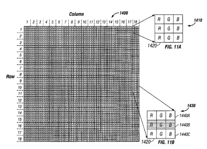
Figures 10, 11A, and 11B are diagrams illustrating an exemplary improved
configuration
of a pixel 1400. The term "total bit depth," as used herein refers to a bit
depth of an entire pixel,
such as pixel 1400, while the term "element bit depth" refers to the bit depth
of a single display
element, such as display elements 1420. The pixel 1400 comprises a plurality
of substantially
equally sized sub-regions having a first group of sub-regions 1410 and a
second group of sub-
regions 1430. Each of the sub-regions 1410 of the first group includes a first
number of display
elements 1420 per color. Each of the sub-regions 1430 of the second group
includes a second
number of display elements 1440 per color. The second number minus the first
number is
substantially equal to two raised to a power that is less than the total bit
depth per color.
More particularly, Figure 10 schematically illustrates a pixel 1400 comprising
an 18 x 18
array of sub-regions which include 18 x 17 = 306 sub-regions 1410
schematically illustrated in
Figure 11A, and 18 sub-regions 1430 schematically illustrated in Figure 11B.
Although the pixel
1400 has significantly fewer sub-regions than does the pixel 100 schematically
illustrated by
Figure 7, both the pixel 1100 of Figure 7 and the pixel 1400 of Figure 10
provide a total bit depth
per color of 13 (n = 13). However, the pixel 1400 includes a reduced number of
sub-regions
-15-
CA 02516915 2005-08-23
compared to the pixel 1100 and, thus, fewer leads are needed to drive the
pixel 1400.
Accordingly, the pixel 1400 provides the same total bit depth as the pixel
1100 with fewer leads
and, thus, reduced loss in aperture when compared to the pixel 1100.
In the exemplary pixel 1400, each sub-region 1410 comprises c display elements
1420
per color. For example, as shown in Figure 1 1A, the sub-region 1410 comprises
c = 3 red display
elements, c = 3 green display elements, and c = 3 blue display elements. The
sub-regions 1410
are arranged in 17 rows in Figure 10, but their configurations are also
compatible with other
embodiments described herein. In general, an array of 18 x 18 sub-regions 1410
would be able to
provide (18 x 18 x 3) + 1 = 973 shades per color, which corresponds to a total
bit depth per color
of 10 (2'°=1024 shades per color).
In order to achieve a total bit depth that is greater than 10 from the above-
introduced 18 x
18 array of sub-regions, additional shades must be made available. For
example, in order to
achieve a total bit depth of 13 in the pixel 1400, 2"/2'° = 8
additional color shades are needed. In
certain embodiments, these additional shades are provided by one or more sub-
regions 1430,
which replace corresponding sub-regions 1410. In Figure 10, for example, the
pixel 1400 is
divided into 18 rows and 18 columns (m=18) of sub-regions, where 17 rows
contain sub-regions
1410 and one row contains sub-regions 1430.
In the exemplary pixel 1400, the sub-regions 1430 are each divided into 11
display
elements. More particularly, the 18 sub-regions 1430 each include two rows of
display elements
1440a that are the same size as the display elements 1420, and 9 rows of
display elements 1440b
that are smaller than the display elements 1420. Thus, each of the sub-regions
1430 has 8 more
display elements per color than does each of the sub-regions 1410. In the
embodiment of Figure
11B, the display elements 1440b are 1/9 the size of the display elements
1440a, 1420.
Accordingly, the display elements 1440b each have an intensity that is
fractional that of the
display elements 1440a, 1420. These smaller display elements 1440b provide 8
additional shades
in between each of the shades that are available without the smaller display
elements 1440b.
Thus, by adding these additional smaller display elements 1440b, the number of
shades provided
by the pixel is increased by a factor of 8. Although the display elements
1440b illustrated in
Figure 10 are formed along a single row of the pixel 1400, in other
embodiments the display
elements 1440b may be dispersed throughout the pixel 1400.
In embodiments where the pixel 1100 and the pixel 1400 are substantially
equally sized,
the display elements 1420 of Figure 11A and 11B are larger than the display
elements 1120 of
Figures 8 and 9, and thus fewer in number. For example, in the embodiment of
Figure 10, the
sub-regions 1410 are approximately 8 times larger than the sub-regions 1110 of
Figure 7 (e.g.,
pixel 1110 includes 522 = 2,704 sub-regions while pixel 1410 includes 182 =
324 sub-regions, so
that sub-regions of the pixel 1410 are larger by a factor of 2,704 / 324 =
8.34). To display the
-16-
CA 02516915 2005-08-23
most significant bit of the display driver signal in pixel 1400 thus requires
activation of 162 (18z /
2) sub-regions 1410 while display of the most significant bit of the display
driver signal in pixel
1100 requires activation of 1352 (522 / 2) sub-regions 1110. This reduction in
the number of sub-
regions needed to produce the shades associated with the most significant bit
of the display driver
signal results in a corresponding reduction in the required number of leads.
Accordingly, the
pixel 1400 has fewer leads than pixel 1100, while providing substantially the
same bit depth per
color.
In certain embodiments, as schematically illustrated by Figure 10, the pixel
1400 is
subdivided into sub-regions configured in an equal number of rows and columns
m. In the
embodiment of Figure 10, pixel 1400 is sub-divided into sub-regions in
accordance with the
following equation:
m2 ~ c + 1 = 2P, (Eqn. 4)
where p is a total bit depth lower than the desired total bit depth, n, e.g.,
p < n. In one
embodiment, p represents a bit depth of a pixel having substantially m2
equally sized display
elements. Thus, in Figure 7, for example, p = n. As will be discussed
hereinafter, a total bit
depth of a pixel having substantially equally sized display elements may be
increased from p to n
by further subdividing one or more display elements into smaller additional
display elements.
These smaller display elements may increase the total bit depth of the pixel
by providing linear
and/or non-linear increments between shades available by the larger display
elements.
In one embodiment, the value of p may be selected such that each of the
individual red,
green, and blue display elements 1420 are distributed with a spatial frequency
that tends not to be
visible to the eye for a given set of viewing conditions and the dynamic range
of the display. In
another embodiment, p may be selected according to a number of leads that the
pixel is
configured to handle, which may be determined by factors of cost and/or the
size of the pixel, for
example. Thus, the value of p may vary from one application to another. In an
exemplary
embodiment discussed herein, p = 8. However, p may be any other value, such as
2, 3, 4, 5, 6, 7,
8, so long as p is less than n.
As noted above, the smaller display elements 1440b produce 2"-P increments
between
adjacent shades so that the total number of shades in the pixel 1400 is 2p ~
2"'P = 2", providing a
total bit depth of n.
Although exemplary pixel 1400 includes an entire row of sub-regions 1430, in
other
embodiments different amounts of sub-regions may be included in a pixel and
the sub-regions
1430 can be dispersed throughout the pixel. In addition, depending on the
values of p and n, the
number of additional divisions necessary to achieve the total bit depth n may
be adjusted.
-17-
CA 02516915 2005-08-23
In certain embodiments having one or more sub-regions 1430, including display
elements
1440b, and multiple sub-regions 1410, including display elements 1420, the
number of leads per
pixel 1400 can be expressed as:
[m ~ c ~ 2] + 2"-p (Eqn. 5)
In other words, the number of leads for the pixel 1400 is equal to the number
leads used
in a pixel having a bit depth of p, plus the 2"-p extra leads necessary to
drive the display elements
1440b. In the exemplary embodiment of Figure 10, the number of leads is [18 ~
3 ~ 2] + 2Os-~0> -
116. For comparison, the pixel 1100 depicted in Figure 7 included 312 leads to
achieve the same
13 bit color depth.
In other embodiments, sub-regions can be divided unequally to form display
elements
1440b that are non-linearly sized, thus providing different levels of color
change depending on
the size of the display elements 1440b that are activated. In such
embodiments, the display
elements 1440b may be used to approximate a certain display response profile,
such as is
typically referred to as gamma.
In other embodiments, the smaller display elements, such as display elements
1440b, may
be formed in other manners than discussed above with reference to Figures 10
and 11B. For
example, the aperture of one or more display elements may be decreased using a
black mask or
other suitable methods as would be apparent to one of skill in the art, to
form the smaller linear or
non-linear display elements. In one embodiment, the aperture of 2"-P display
elements may be
decreased in order to achieve a desired total bit depth. In this embodiment,
the number of display
elements with a decreased aperture is only a small fraction of the total
number of display
elements and, thus, the decrease in the total aperture of the pixel is
generally not significant.
Figure 12 is a diagram illustrating another exemplary sub-region architecture
that may be
implemented to achieve a desired total bit depth with a reduced number of
leads. In the
embodiment of Figure 12, a pixel 1600 is divided into an array of sub-regions
1610 that
correspond to the most significant bits of the drive signal, e.g., those that
cover a substantial
portion of the total aperture of the pixel 1600. In certain embodiments, the
array of sub-regions
1610 covers more than about 90% of the total aperture of the pixel 1600. In
certain other
embodiments, the array of sub-regions 1610 covers more than about 98% of the
total aperture of
the pixel 1600. In certain other embodiments, the fraction of the total
aperture of the pixel 1600
covered by the array of sub-regions 1610 is in a range between approximately
85% and
approximately 100%. As described below, these sub-regions 1610 are distributed
such that there
is generally very small loss of aperture corresponding to these significant
signal bits. The
remaining portion, or less significant bits, of the drive signal are used to
drive smaller display
elements 1636. Because of the reduced size of the display elements 1636, more
leads for a given
-18-
CA 02516915 2005-08-23
area of display elements 1636 are necessary than for an equally sized area of
the larger sub-
regions 1610. Accordingly, the display elements 1636 generally exhibit a
greater percentage loss
of aperture associated with these less significant portions of the signal. As
these less significant
bits of the display signal are associated with a much smaller portion of the
aperture of the pixel
1100 (less than 10%, for example), this loss is insignificant. In one
embodiment, the pixel 1600
is subdivided into sub-regions according to the formula:
N ~ M = 2K+i - 4 (Eqn. 6)
where integer N is the number of sub-regions 1610 in a row of the pixel 1600,
integer M is the
number of sub-regions 1610 in a column of the pixel 1600, and integer K is the
number of bits of
the signal that are designated as "significant bits." These K bits of the
drive signal drive the
display elements that are considered most significant in the pixel 1600, which
are typically the
larger display elements that generate the most frequently used shades or
colors. The remaining
bits of the drive signal drive display elements are fit into a remaining
portion of the pixel 1600.
The display elements in this remaining portion may be sized by reducing their
effective aperture.
In this way, these smaller aperture display elements can represent the proper
binary weights and,
because of their relatively small apertures, the area they consume is
relatively inconsequential. In
one embodiment, the display elements driven by the less significant bits are
disposed in a cross
shape area that divides the pixel into quadrants as schematically illustrated
by Figure 12.
In the pixel 100 of Figure 7, for example, the most significant bit of the
display driver
signal may correspond to switching half of the equal sized sub-regions 1110.
The switching of
half of the sub-regions 1110 of a simple binary grid requires a signal from a
corresponding half of
the leads in such a pixel architecture. Thus, reducing the number of sub-
regions associated with
the most significant bits of the display driver signal can allow the number of
leads to be reduced.
Some pixel architectures use sub-regions having a geometrically increasing
area to produce the
output from the least to most significant bit of the control signal. This
architecture can reduce
lead count substantially. However, as discussed above, the large sub-regions
in such displays
may create display artifacts in large area displays, e.g., where the large sub-
regions are visible
within the pixel to a viewer.
In the exemplary embodiment of Figure 12, the pixel 1600 provides a total bit
depth of
13, while reducing the number of leads for the display driver signal from that
discussed above
with respect to the 13-bit pixel 1100. To achieve a total bit depth of 13, the
driver signal
comprises 13 bits, including some significant bits and some less significant
bits. The exemplary
pixel 1600 is divided such that N = 18, M = 14, and K = 6, so that the pixel
includes 252 (18 ~ 14
= 252) sub-regions 1610 and the driver signal includes 6 significant bits and
7 less significant
bits. Those of skill in the art will recognize that this number of rows and
columns is exemplary
-19-
CA 02516915 2005-08-23
and that in other embodiments the number of rows and columns may vary as
discussed above. Of
the 252 sub-regions 1610 in this embodiment, 128 sub-regions (labeled "Bit 1")
are configured to
be activated by the most significant bit of the driver signal, 64 sub-regions
(labeled "Bit 2") are
configured to be activated by the second most significant bit, 32 sub-regions
(labeled "Bit 3") are
configured to be activated by the third most significant bit, 16 sub-regions
(labeled "Bit 4") are
configured to be activated by the fourth most significant bit, 8 sub-regions
(labeled "Bit 5") are
configured to be activated by the fifth most significant bit, and four sub-
regions (labeled "Bit 6")
are configured to be activated by the sixth most significant bit.
For a color display, each of the sub-regions 1610 may be further divided into
display
elements for each of the primary colors. For example, one embodiment may use
the staggered
arrangement depicted in Figure 8. In the exemplary embodiment of Figure 12,
the sub-regions
1610 are approximately 10 times larger than the sub-regions of the embodiment
of Figure 7. To
display the most significant bit of the display driver signal thus requires
activation of only 128
sub-regions 1610 rather than activation of 1352 sub-regions 1110 as in the
embodiment of
Figure 7.
In the embodiment depicted in Figure 12, the row and column layout of sub-
regions is
divided into four quadrants 1630 that are separated by a cross shaped area
1632. The cross
shaped area can be further divided into sub-regions 1634. The remaining seven
(in a 13 bit color
depth embodiment) "less significant bits" are used to drive the display
elements in sub-regions
1634. In one embodiment, the small central sub-region 1636 may be left unused
leaving 32 sub-
regions 1632. In one embodiment, the first less significant bit, e.g., bit
seven, can be used to
drive 11 of these small sub-regions 1634, bit eight can be used to drive 7 sub-
regions 1634, bit
nine can be used to drive 4 sub-regions 1634, and bit ten can be used to drive
2 sub-regions 1634.
In one embodiment, bits 11, 12, and 13 are each used to drive one sub-region
1634 each. Thus 27
of the 32 cross-hair sub-regions 1634 are driven by the less significant bits.
Since these "less
significant bits" do not fill all of the crosshair sub-regions 1634, their
exact size can be adjusted
to achieve precise binary weighting. The impact of these unused and partially
used sub-regions
1634 on the overall aperture is approximately 0.1% and is thus generally
insignificant. However,
the simplification in sub-region layout, e.g. grouping the sub-regions 1634
associated with the
less significant bits into a single row and/or column, allows for a further
reduction in lead count.
In other embodiments, the size of the sub-regions 1634 may be adjusted to
achieve various linear
and non-linear gradations. In addition, other embodiments may include more or
less sub-regions
1634 and the sub-regions 1634 may be dispersed in other manners throughout the
pixel.
The lead count for the pixel 1600 illustrated by Figure 12 can be
characterized as:
N + [M ~ c] + 1 + 3 (Eqn. 7)
-20-
CA 02516915 2005-08-23
where N represents the leads for each horizontal sub-pixel, M ~ c represents
the leads for each
color of each vertical sub-pixel, the additional 1 represents the horizontal
crosshair lead, and the
additional 3 represents the vertical crosshair leads. Thus, with specific
reference to the
embodiment described above, the total lead count is 14 + (18 ~ 3) +1 + 3 = 72.
This compares
very favorably to 312 leads used in the equivalent 13 bit-depth embodiment
depicted in Figure 7.
Since the pixels driven by the "most significant bits" can be kept relatively
large,
embodiments of this pixel architecture can have high aperture ratios when
working with crude
design rules. In addition, the artifacts associated with using large pixels,
as for example in a large
display such as a billboard, can be minimized by distributing one quarter of
the sub-regions 1610
assigned to each "most significant" bit across each of the four quadrants 1630
of the pixel 1600.
This causes the output energy perceived by the viewer to appear to be coming
from across the
entire surface of the pixel 1600 and limits the viewer's ability to pick out
isolated bright dots
from these sub-regions 1610, which may be perceived as artifacts or noise in
the displayed image.
Figures 13A and 13B are system block diagrams illustrating an embodiment of a
display
IS device 2040. The display device 2040 can be, for example, a cellular or
mobile telephone.
However, the same components of display device 2040 or slight variations
thereof are also
illustrative of various types of display devices such as televisions and
portable media players.
The display device 2040 includes a housing 2041, a display 2030, an antenna
2043, a
speaker 2045, an input device 2048, and a microphone 2046. The housing 2041 is
generally
formed from any of a variety of manufacturing processes as are well known to
those of skill in
the art, including injection molding, and vacuum forming. In addition, the
housing 2041 may be
made from any of a variety of materials, including but not limited to plastic,
metal, glass, rubber,
and ceramic, or a combination thereof. In one embodiment the housing 2041
includes removable
portions (not shown) that may be interchanged with other removable portions of
different color,
or containing different logos, pictures, or symbols.
The display 2030 of exemplary display device 2040 may be any of a variety of
displays,
including a bi-stable display, as described herein. In other embodiments, the
display 2030
includes a flat-panel display, such as plasma, EL, OLED, STN LCD, or TFT LCD
as described
above, or a non-flat-panel display, such as a CRT or other tube device, as is
well known to those
of skill in the art. However, for purposes of describing the present
embodiment, the display 2030
includes an interferometric modulator display, as described herein.
The components of one embodiment of exemplary display device 2040 are
schematically
illustrated in Figure 13B. The illustrated exemplary display device 2040
includes a housing 2041
and can include additional components at least partially enclosed therein. For
example, in one
embodiment, the exemplary display device 2040 includes a network interface
2027 that includes
an antenna 2043 which is coupled to a transceiver 2047. The transceiver 2047
is connected to the
-21-
CA 02516915 2005-08-23
processor 2021, which is connected to conditioning hardware 2052. The
conditioning hardware
2052 may be configured to condition a signal (e.g. filter a signal). The
conditioning hardware
2052 is connected to a speaker 2045 and a microphone 2046. The processor 2021
is also
connected to an input device 2048 and a driver controller 2029. The driver
controller 2029 is
coupled to a frame buffer 2028 and to the array driver 2022, which in turn is
coupled to a display
array 2030. A power supply 2050 provides power to all components as required
by the particular
exemplary display device 2040 design.
The network interface 2027 includes the antenna 2043 and the transceiver 2047
so that
the exemplary display device 2040 can communicate with one or more devices
over a network.
In one embodiment the network interface 2027 may also have some processing
capabilities to
relieve requirements of the processor 2021. The antenna 2043 is any antenna
known to those of
skill in the art for transmitting and receiving signals. In one embodiment,
the antenna transmits
and receives RF signals according to the IEEE 802.11 standard, including IEEE
802.11 (a), (b), or
(g). In another embodiment, the antenna transmits and receives RF signals
according to the
BLUETOOTH standard. In the case of a cellular telephone, the antenna is
designed to receive
CDMA, GSM, AMPS or other known signals that are used to communicate within a
wireless cell
phone network. The transceiver 2047 pre-processes the signals received from
the antenna 2043
so that they may be received by and further manipulated by the processor 2021.
The transceiver
2047 also processes signals received from the processor 2021 so that they may
be transmitted
from the exemplary display device 2040 via the antenna 2043.
In an alternative embodiment, the transceiver 2047 can be replaced by a
receiver. In yet
another alternative embodiment, network interface 2027 can be replaced by an
image source,
which can store or generate image data to be sent to the processor 2021. For
example, the image
source can be a digital video disc (DVD) or a hard-disc drive that contains
image data, or a
software module that generates image data.
Processor 2021 generally controls the overall operation of the exemplary
display device
2040. The processor 2021 receives data, such as compressed image data from the
network
interface 2027 or an image source, and processes the data into raw image data
or into a format
that is readily processed into raw image data. The processor 2021 then sends
the processed data
to the driver controller 2029 or to frame buffer 2028 for storage. Raw data
typically refers to the
information that identifies the image characteristics at each location within
an image. For
example, such image characteristics can include color, saturation, and gray-
scale level.
In one embodiment, the processor 2021 includes a microcontroller, CPU, or
logic unit to
control operation of the exemplary display device 2040. Conditioning hardware
2052 generally
includes amplifiers and filters for transmitting signals to the speaker 2045,
and for receiving
signals from the microphone 2046. Conditioning hardware 2052 may be discrete
components
-22-
CA 02516915 2005-08-23
within the exemplary display device 2040, or may be incorporated within the
processor 2021 or
other components.
The driver controller 2029 takes the raw image data generated by the processor
2021
either directly from the processor 2021 or from the frame buffer 2028 and
reformats the raw
image data appropriately for high speed transmission to the array driver 2022.
Specifically, the
driver controller 2029 reformats the raw image data into a data flow having a
raster-like format,
such that it has a time order suitable for scanning across the display array
2030. Then the driver
controller 2029 sends the formatted information to the array driver 2022.
Although a driver
controller 2029, such as a LCD controller, is often associated with the system
processor 2021 as a
stand-alone Integrated Circuit (IC), such controllers may be implemented in
many ways. They
may be embedded in the processor 2021 as hardware, embedded in the processor
2021 as
so8ware, or fully integrated in hardware with the array driver 2022.
Typically, the array driver 2022 receives the formatted information from the
driver
controller 2029 and reformats the video data into a parallel set of waveforms
that are applied
I S many times per second to the hundreds and sometimes thousands of leads
coming from the
display's x-y matrix of pixels.
In one embodiment, the driver controller 2029, array driver 2022, and display
array 2030
are appropriate for any of the types of displays described herein. For
example, in one
embodiment, driver controller 2029 is a conventional display controller or a
bi-stable display
controller (e.g., an interferometric modulator controller). In another
embodiment, array driver
2022 is a conventional driver or a bi-stable display driver (e.g., an
interferometric modulator
display). In one embodiment, a driver controller 2029 is integrated with the
array driver 2022.
Such an embodiment is common in highly integrated systems such as cellular
phones, watches,
and other small area displays. In yet another embodiment, display array 2030
is a typical display
array or a bi-stable display array (e.g., a display including an array of
interferometric
modulators).
The input device 2048 allows a user to control the operation of the exemplary
display
device 2040. In one embodiment, input device 2048 includes a keypad, such as a
QWERTY
keyboard or a telephone keypad, a button, a switch, a touch-sensitive screen,
a pressure- or heat-
sensitive membrane. In one embodiment, the microphone 2046 is an input device
for the
exemplary display device 2040. When the microphone 2046 is used to input data
to the device,
voice commands may be provided by a user for controlling operations of the
exemplary display
device 2040.
Power supply 2050 can include a variety of energy storage devices as are well
known in
the art. For example, in one embodiment, power supply 2050 is a rechargeable
battery, such as a
nickel-cadmium battery or a lithium ion battery. In another embodiment, power
supply 2050 is a
-23-
CA 02516915 2005-08-23
renewable energy source, a capacitor, or a solar cell, including a plastic
solar cell, and solar-cell
paint. In another embodiment, power supply 2050 is configured to receive power
from a wall
outlet.
In some implementations control programmability resides, as described above,
in a driver
controller which can be located in several places in the electronic display
system. In some cases
control programmability resides in the array driver 2022. Those of skill in
the art will recognize
that the above-described optimization may be implemented in any number of
hardware and/or
software components and in various configurations.
While the above detailed description has shown, described, and pointed out
novel
features of the invention as applied to various embodiments, it will be
understood that various
omissions, substitutions, and changes in the form and details of the device or
process illustrated
may be made by those skilled in the art without departing from the spirit of
the invention. As will
be recognized, the present invention may be embodied within a form that does
not provide all of
the features and benefits set forth herein, as some features may be used or
practiced separately
from others.
-24-