Note: Descriptions are shown in the official language in which they were submitted.
CA 02517009 2005-08-19
WO 2004/077580 PCT/US2004/005650
COMPOSITE WHITE LIGHT SOURCE AND METHOD FOR FABRICATING
[0001] This application claims the benefit of U.S.
Provisional Application Serial No. 60/451,067 filed
February 26, 2003.
BACKGROUND OF THE INVENTION
Field of the Invention
[0002] This invention relates to light emitters and, more
particularly, to light emitters where the wavelength of
at least some of the emitted light is converted to
another wavelength by a conversion material region.
Description of the Related Art
[0003] Light emitting diodes (LEDs) are an important
class of solid-state devices that convert electric energy
to light energy and generally comprise an active layer of
semiconductor material sandwiched between two appositely
doped layers. When a bias is applied across the doped
layers, holes and electrons are injected into the active
layer where they recombine to generate light. Light is
typically emitted omnidirectionally from the active layer
and from the surfaces of the LED.
[0004] One disadvantage of conventional LEDs used for
lighting applications is that they cannot generate white
light from their active layers. One way to cause a
single blue emitting LED to emit white light is to
surround it with a yellow phosphor, polymer or dye. [See
CA 02517009 2005-08-19
WO 2004/077580 PCT/US2004/005650
2
Nichia Corp. white LED, Part No. NSPW300BS, NSPW312BS,
etc.; See also U.S. Patent No. 5959316 to Hayden,
"Multiple Encapsulation of Phosphor-LED Devices"]. The
surrounding material "downconverts" the wavelength of at
least some of the light, changing its color, For
example, if a blue emitting LED is surrounded by a yellow
phosphor, then some of the blue light passes through the
phosphor without being changed while the remaining light
is downconverted to yellow. Hence, the LED emits both
blue and yellow light, which combines to form a white
light.
[0005] One conventional method for manufacturing an LED
surrounded by a conversion material region is to mount
the LED in a cup shaped submount with the necessary
electrical connections to apply a bias to the LED. A
syringe mechanism is filled with an optically clear and
curable material (e. g. epoxy, silicon, sol gel, etc.)
with the conversion material mixed in the material, where
the conversion material typically includes phosphor
particles. The syringe mixture is then injected into the
submount, covering the LED and partially filling the
submount. When the clear material is first injected into
the cup, the conversion particles are generally uniformly
mixed/suspended throughout the material. The clear
material is then cured to form the conversion material
region and the entire assembly is encased in a clear
epoxy.
[00062 One disadvantage of this manufacturing method is
that under certain circumstances the conversion particles
can be non-uniformly distributed in the cured state.
After the clear material mixture is inj ected into a cup,
CA 02517009 2005-08-19
WO 2004/077580 PCT/US2004/005650
3
there can be a time delay before it is cured. During
this delay, the conversion particles Can settle toward
the base of the cup and over the LED such that there are
different concentrations of particles throughout the
conversion material region. This settling problem can be
compounded in clear materials that dehydrate during the
curing process, which allows the conversion particles to
settle more quickly. The settled conversion material
region can result in light from the emitter appearing as
different colors and/or intensities when viewed from
different angles because the emitted light encounters
different amounts of conversion material.
[0007 Another disadvantage of this method is that the
injection of the optically clear material from a syringe
can introduce variations in the concentration of
conversion particles from emitter to emitter, which can
reduce the consistent reproducilaility of the emitters.
The conversion particles can settle in the sy~:inge such
that emitters injected with the clear material mixture
when the syringe is full can have a greater concentration
of con~be~:sion pazticles than emitters formed later . The
amount of clear material injected from the syringe into
the cup can also be difficult to control and different
amounts of clear material mixture can be deposited in
different emitters. This can also result in different
amounts of conversion particles in different emitters.
The end surface shape of the cured material can also vary
such that light from different LEDs pass through
different amounts of clear material and particles, These
problems reduce the ability to manufacture emitters with
consistent light emission characteristics.
CA 02517009 2005-08-19
WO 2004/077580 PCT/US2004/005650
4
[0008 .Another disadvantage of the conventional emitter
manufacturing method is the waste of material when the
emitter does not meet the necessary emission standards.
There is no practical method for separating the two so
the entire emitter must be discarded if the emitter or
the conversion material region is defective. Hence, if
the LED is good but the conversion material region is
defective, then both will be unusable. Discarding the
entire emitter results in the excessive wasting of
otherwise good LEDs, which can add to the overall cost of
manufacturing.
SUMMARY ~F THE INVENTI~N
(000~~ The present invention provides an improved LED
based emitter anal. method for fabricating an emitter that
addresses the disadvantages of conventional emitters and
methods. ~ne embodiment of an emitter according to the
present invention comprises a light source which emits a
first sgectrum o~ light. A conversion material region is
included that is formed separ~.tely from said light source
and includes conversion particles. The conversion
material regir~n is positioned in proximity to the light
source such that at least some of the light source light
passes through the conversion material region.. The
conversion particles absorb at least some of the light
source light passing through the conversion material
region and emitting a second spectrum of light.
(0010a Another embodiment of an emitter according to the
present invention comprises a light source which emits a
first spectrum of light and a conversion material region
CA 02517009 2005-08-19
WO 2004/077580 PCT/US2004/005650
formed separately from said light source. The conversion
material region is positioned proximate to the light
source and arranged to absorb at least some of the light
emitted by the light source and re-emit light at a second
spectrum of light. The emitter emits a combination of
the first and second spectrums of light in a uniform
third spectrum of light.
[0011] One embodiment of a method of fabricating an
emitter according to the present invention comprises
providing a light source and providing a separately
formed conversion. material region which includes
conversion particles. The conversion material region is
then bonded proximate to the light source. The
conversion material region is positioned so that at least
some of the light emitted fr~m the light source at
different angles flows thr~ugh said conversion material
region and throt~.gh the substantially the same amount of
conversion particles.
[0012] These and other further features and advantages of
the invention would be apparent to those skilled in the
art fr~m the foilowing detailed description, taping
together with the accompanying drawings, in which:
ERIEF DESCRIPTION OF THE DRAWINGS
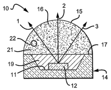
[0013] FIG. ~. is a sectional view of one embodiment of a
light emitter according to the present invention having a
hemispheric shaped phosphor-containing lens that is
manufactured separately from the LED and submount;
[0014] FIG. 2 is a sectional view of the emitter of FIG.
2, with the separate pieces banded together;
CA 02517009 2005-08-19
WO 2004/077580 PCT/US2004/005650
6
(0015] FIG. 3 is a sectional view of another embodiment
of an emitter according to the present invention having a
dome shaped phosphor-containing lens;
[0016] FIG. 4 is a sectional view of the emitter of FIG.
3, with the separate pieces bonded together;
[0017) FIG. 5 is a sectional view of another embodiment
of an emitter according to the present invention having a
dome shaped phosphor-containing lens;
[0018] FIG. 6 is a sectional view of the emitter of FIG.
with the separate pieces bonded together;
[0019] FIG. 7 is a sectional view of another embodiment
of an emitter according to the present invention having a
dome shaped phosphor-containing lens;
[0020) FIG. 8 is a sectional view of the emitter of FIG.
7 with the separate pieces bonded together;
[0021] FIG. 9 is a sectional view ~f another embodiment
of an emitter according to the present invention having a
hemispheric lens with a phosphor-containing layer and
scattering particles;
[0022] FIG. 1Q is a sectional view of the emitter of FIG.
9 with the separate pieces bonded together;
[002] FIG. 11 is a sectional view of another embodiment
of an emitter according to the present invention having a
generally hemispheric lens with a phosphor-containing
layer;
[0024] FIG. 12 is a sectional view of the emitter of FIG.
11 with the separate pieces bonded together;
[0025] FIG. 7.3 is a sectional view of another embodiment
of an emitter according to the present invention having a
phosphor-loaded cap;
CA 02517009 2005-08-19
WO 2004/077580 PCT/US2004/005650
7
L0026] FIG. 14 is a sectional view of the emitter of FIG.
13 with the separate pieces bonded together;
[00271 FIG. 15 is a sectional view of another embodiment
of an emitter according to the present invention having a
perforated phosphor loaded cap;
[0028] FIG. 16 is a sectional view of the emitter of FIG.
15 with the separate pieces bonded together; and
[0029] FIGS. 17 and 18 are flow diagrams illustrating
methods of fabricating an emitter according to the
present invention.
DETAILED DESCRIPTION ~F THE INVENTIQN
00030] FIGS. 1 and 2 illustrate one embodiment of a light
emitter 10 in accordance with the present invention.
Emitter 10 can be used in many different applications
such as being included in a. display s~rste~n where it is
desired to emit light at a uniform color and/or intensity
through a range of angles. The system can include a
single emitter or a.n array of emitters, but one emitter
is illustrated here foe simplicity and ease of
discussion.
[0031] Emitter 10 includes a light source Z2 positioned
on a surface 11 of a cup shaped submount 14. Light
source 12 can be mounted on surface 11 using known
bonding methods. A filler material 19 is positioned on
surface 11 and surrounds light source 12 so that filler
material 19 fills the volume within the cup. A
hemispheric lens 16, which includes phosphor, is
positioned adjacent to submount 14. Lens 16 includes
conversion particles 22 distributed throughout so that
CA 02517009 2005-08-19
WO 2004/077580 PCT/US2004/005650
8
lens 16 and particles 22 form a conversion material
region 21. Surface 11 can be reflective at the
wavelengths of interest so that light emitted by light
source 12 reflects from surface 11 and contributes to the
light emission of emitter 10. It should be noted that
conversion particles 22 are represented as dots in lens
16 as shown in FIGS. 1 and 2, and the rest of the figures
shown in this disclosure.
[0032] A surface 13 of lens 16 bonds to filler material
19 and is held in place relative to submount 14. Hence,
lens 16 is positioned so that a portion of the light
emitted lay' light source 12 flows through lens 16 from
surface 13 to a surface 15. However, filler material 19
is optional and lens 16 can be bonded directly to a
surface 17 of submount 14. Filler material 19 can
include an epoxy or another filler material capable of
bonding lens 16 to submount 14. Lens 16 and filler
material 19 can include a material transparent to the
wavelengths of interest. Conversion particles 22 can
include one or more fluorescent or phosphorescent
materials such as a phospl2or, a fluorescent dye, or a
photoluminescent semiconductor material.
[0033] As shown, light source 12 includes a single light
emitting diode (LED). However, light source 12 can
include other light emitters, such as a solid-state
laser, a laser diode, an organic light emitting diode,
among others. The desired wavelengths of interest
typically range from the infrared to the ultraviolet
regions, although other wavelengths could be used.
Further, light source 12 can include multiple light
CA 02517009 2005-08-19
WO 2004/077580 PCT/US2004/005650
9
sources which emit light at the same or different
wavelengths.
(0034] The operation and fabrication details of
conventional LEDs and other light emitters are known and
are only briefly discussed. Conventional LEDs can be
fabricated from a number of material systems by many
known methods, with a suitable method being fabrication
by Chemical Vapor Deposition (CVD). Other suitable
methods include Molecular Beam Epitaxy (MBE) and Metal
Organic Chemical Vapor Deposition (MOCVD).
(0035] LEDs typically include an active region sandwiched
between two oppositely doped layers that are either doped
p-type or n-type. The top layer of the LED is usually p-
type and the bottom layer is usually n-type, although
LEDs also work if the conductivities of the layers are
reversed. The p- and n-type layers have respective
contacts and an electrical signal can be applied across
the contests so that a current is injected into the
active region to produce light emission.
(0036] Submount 14 can include electrical circuitry (not
shown) coupled to light sou~:ce 12, such as electrical
circuitry to provide power for lic-~ht emission. Submount
14 can also include components and circuitry to protect
light source 12 from large electrical signals such as
electrostatic shock.
(0037] In operation, light source 12 emits light at a
desired wavelength where the emitted light flows through
lens 16 either directly from the light source or
indirectly by reflection from surface 11. A portion of
the light emitted by light source 12 flows through lens
16 and is absorbed by conversion particles 22
CA 02517009 2005-08-19
WO 2004/077580 PCT/US2004/005650
[0038] A portion of the absorbed radiation is re-emitted
at one or more wavelength spectrums which are generally
different from the absorbed wavelength, with the re-
emitted light typically having a longer wavelength than
the absorbed light. The combination of the transmitted
light and the retransmitted light allows the emitter 10
to emit different wavelengths of light than the original
emitted light. For example, light source 12 can emit
blue light and conversion particles 22 can absorb a
portion of the blue light and convert it to yellow light.
The emitter 10 then emits a white light combination of
The blue and yellow light . A full range of broad yellow
spectral emission is possible using conversion particles
which include phosphors based on the (Gd,Y~3(Al,Ga?s~ia:Ce
system. In another example, conversion particles 22 can
re-emit green light, with a suitable green emitting
material being a Sr:thiogallate phosphor. Other
conversion particles can be used that absorb blue light
and re-emit at different wavelengths of light. Different
conversion particles can. also be used that absorb
different wavelengths of light and re-emit light at
different wavelengths, such as particles the absorb
ultra-violet light and emit light at a different
wavelength.
[0039] In accordance with the invention, it is desired to
distribute conversion particles 22 uniformly throughout
lens 16 so that the color and the intensity of the
emitted light is uniform throughout a wide range of
viewing angles. Consequently, lens 16 is fabricated
separately from submount 14 and light source 12. Hence,
instead of injecting the clear material mixture which
CA 02517009 2005-08-19
WO 2004/077580 PCT/US2004/005650
11
forms lens 16 into submount 14, material can be used to
mass produce lenses using known methods such as injection
molding or the conventional syringe manufacturing
process. By fabricating lens 16 separately from submount
14 and light source 12, a number of advantages are
realized that overcome problems associated with emitters
manufactured using conventional methods.
L0040~ One advantage is that the manufacturing process
can provide lenses which are less expensive than
conventional techniques. One reason the process is less
expensive is because the formation of emitter 10 reduces
the waste generated since light source 12 can be tested
before lens 16 is bonded onto submount 14. If emitter 10
has substandard emission or is otherwise defective, then
a determination can be made as to whether light source l2
or lens 16 is defective. The defective component can
then be discarded and substituted with a new component.
The replacement process avoids the waste associated with
the conventional manufacturing processes where the entire
emitter is discarded if the emission is substandard.
L00~~~~ x'~noth.er advantage is that the emitters can be
formed with a more flexible manufacturing process. for
example, different lenses can be used to match the
geometry of submount 14 and light source 12. Also, the
color emitted by a particular emitter 10 can be changed
by using a lens which includes a different type of
conversion particles to produce different light
combinations . The changing of lenses can be done at the
assembly line by simply substituting a different supply
of lenses.
CA 02517009 2005-08-19
WO 2004/077580 PCT/US2004/005650
12
[0042 Flexibility in the manufacturing process is also
obtained because a wider selection of materials can be
used to form lens 16. For example, because the clear
material is injected directly on the LED in the
conventional syringe method, only material with a
relatively low melting/curing temperature can be used.
If higher temperature materials are used, then light
source 12 or submount 14 can be damaged when contacted by
the clear material mixture.
[0043 Lens 16 is manufactured separate from light source
12 and submount 14 and then bonded to submount 14 as
discussed above. As a result, materials that might
otherwise cause damage in the conventional syringe
process can now be used, one such material being glass.
By encasing conversion particles 22 in a rugged material
such as glass, conversion particles 22 are better
protected from contaminants in the ambient atc~osphere
that can undesirably react with particles 22 and reduce
the usable lifetime of emitter 10. It should be
understood that the lens 16 ce.n be made of many different
materials beyond glass, such as an epoxy or pl2atic, and
the invention is not limited to the particular lens
materials mentioned herein.
[0044) The manufacturing process also has the advantage
that the light is emitted with a more uniform color,
intensity, and temperature than provided by conventional
manu.f acturing techniques. One reason better uniformity
is achieved is because the light emitted from source 12
at different angles passes through similar thicknesses of
lens 16 and, accordingly, through substantially similar
amounts of conversion particles 22 since they are have
CA 02517009 2005-08-19
WO 2004/077580 PCT/US2004/005650
13
substantially uniform distribution throughout region 21.
For example, as shown in FTG. 2, light paths 1, 2, and 3
travels through substantially the same thickness of lens
16 and through substantially the same amount of
conversion particles.
[0045] The uniformity of conversion particles 22 is
better controlled since lens 16 is formed separately.
The settling of conversion particles 22 can be avoided by
quickly curing the material mixture after the mixture is
injected into the mold or by shaking the injection mold
during curing.
[0046] Another advantage is that conversion material
region 21 does not generally contact light source 12, so
variations in the surface or shape of light source 12
will not significantly impact the performance of emitter
10. Further, heat can damage conversion particles 22 if
conversion material region 21 is positioned too close to
light source 12.
[0047] FIGS. 3 and 4 illustrate an embodiment of an
emitter 30 in accordance with the present invention.. It
should be noted ths.t emitter 30 includes components
similar to the components illustrated in FIGS. 1 and 2.
Similar numbering is used on similar Components with the
understanding that the discussion above in conjunction
with. emitter 10 applies equally to emitter 30 and the
other embodiments discussed in the rest of the
disclosure.
[0048] Emitter 30 includes light source 12 mounted to
submount 14. Filler material 19 can be positioned on
surface 11 to surround light source 12, but is left out
here and in the rest of the figures for simplicity and
CA 02517009 2005-08-19
WO 2004/077580 PCT/US2004/005650
14
ease of discussion. Emitter 30 includes a lens 36
mounted to surface 17. Lens 36 includes an inside layer
38 with conversion particles 22 and an outside layer 40,
where layers 38 and 40 preferably have uniform
thicknesses throughout. Lens 36 is dome shaped and is
positioned on surface 17 so that a portion of the light
emitted from light source 12 flows through lens 36 from a
surface 33 to a surface 35.
[0049] Conversion particles 22 are distributed throughout
conversion material region 21. However, conversion
material region 21 includes only a portion of lens 36.
In particular, Conversion particles 22 are distributed
throughout inside layer 38 and preferably not within
outside layer 40. Hence, inside layer 38 can include
clear material mixed with. conversion particles 22 and
outside layer 40 can include clear material. In this
arrangement, light emitted at different angles from light
source 12 passes through nearly the same thickness of
lens 36 and the same amount of conversion particles 22.
(i.a. lfight paths 1, 2, and 3 a.re equal)
[~0~~~ Ey forming lens 36 in the shape of e. dome, an
inside distance 42 (See EIG. 4) can. be maintained between
light source 12 and inside layer 38 and conversion
particles 22, with distance 42 being optimised for the
particular light source 12 and submount 14. The optimum
value for distances 42 and thickness 44 depends on the
type and dimensions of light source 12 and submount 14.
Distance 42 is chosen to allow for light source 12 to
provide a higher intensity of light without generating
excessive heat which can damage conversion particles 22.
Heat can damage conversion particles 22 if conversion
CA 02517009 2005-08-19
WO 2004/077580 PCT/US2004/005650
material region 21 is positioned too close to light
source 12.
[0051 Distance 42 can also affect the light efficiency
of emitter 30. When directional light from light source
12 passes into inner layer 38 and is redirected back
towards light source 12, a portion of the directional
light can be absorbed by conversion particles 22 and re-
emitted omnidirectionally. If distance 42 is too small
or if conversion particles 22 are positioned directly on
light source 12, then some of the re-emitted light can be
directed back into and absorbed by light source 12. The
absorption of this light can reduce the overall light
emitting efficiency of emitter 30 because it can increase
the temperature of light source 12. If distance 42 is
too large, then thiclsness 44 can be reduced to a point
that light from conversion particles 22 can be trapped in
lens 36 by total internal reflection, whieh also reduces
the overall efficiency of emitter 30.
[0052 FIGS. 5 and 6 illustrate an emitter 50 in
accordance with the present invention, where emitter 50
includes a flat submount 5~~. In this embodiment, a dome
shaped lens 56 is positioned over light source 12 and
mounted to a surface 51 of submount 54, with light source
12 arranged in the space provided between an inside
surface 53 of lens 56 and submount 54 (See FIG. 6).
Light source 12 and inside surface 53 can be spaced apart
such that the absorption by light source 12 of re-emitted
light from conversion material regions 22 is minimized.
Lens 56 includes conversion particles 22 distributed
throughout lens 56 such that when light emitted from
light source 12 passes through lens 56, a portion of it
CA 02517009 2005-08-19
WO 2004/077580 PCT/US2004/005650
16
is absorbed by conversion particles 22 and re-emitted at
a different wavelength.
[0053) FIGS. 7 and 8 illustrate an embodiment of an
emitter 70 in accordance with the present invention. In
this embodiment, emitter 70 includes a dome shaped lens
76 mounted to surface 5l of submount 54. Lens 76
includes an inside layer 78 which has clear material
mixed with conversion particles 22 arid an outside layer
80 which has clear material, preferably without any
conversion particles. Light flow is from light source 12
through lens 76 from a surface 73 to a surface 75.
[0054 As discussed above in conjunction with FIGS. 3 and
4, an inside distance 82 is chosen between light source
12 and inside layer 78 to minimize the absorption of re-
emitted light from conversion particles 22 into light
source 12. Distance 82 and thickness 84 can be chosen to
optimize the light efficiency of emitter 50 where the
light efficiency is optimized by minimizing the
absorption of the re-emitted light and by reducing the
total internal reflection as discussed. above.
[0055 FIGS. 9 and 10 illustrate an embodiment of an
emitter 90 in. accordance with the present invention where
emitter 90 includes light source 12 mounted to surface 11
of submount 14. In this embodiment, a hemispheric shaped
lens 96 is mounted to surface 17 where lens 96 includes a
bottom layer 98 with conversion particles 22. However,
in addition to conversion particles 22 being distributed
throughout layer 98, layer 98 also includes scattering
particles 100 for redirecting some of the light.
[0056 A portion of the light absorbed and re-emitted by
conversion particles 22 in layer 98 is directed along
CA 02517009 2005-08-19
WO 2004/077580 PCT/US2004/005650
17
layer 98, as shown by arrow 99 (See FIG. 10). This re-
emitted light can be directed away from surface 95.
Hence, one reason scattering particles 100 are included
in layer 98 is to redirect the light towards surface 95
so that the light emitting efficiency of emitter 90 is
increased.
[0057 The conversion and scattering efficiency of
conversion particles 22 can depend on the wavelength of
the light arid the size of the conversion particles.
Conversion material region 21 typically does not scatter
light effectively because the conversion efficiency of
particles 22 decreases as their size decreases. As a
result, it is difficult to obtain high conversion
efficiency particles that are smaller than approximately
one micron in diameter. To effectively scatter light,
the diameter of scatte~:ing particles 100 should be
approximately one half of the wavelength of the light
being scattered. In air, this would result in particles
100 being approximately 0.2 to 0.25 microns in diameter.
This range of diameters would be smaller for particles in
a different medium, such as epoxy or another material
with. an index of refraction greater than free space. As
a result, phosphor particles are generally too large to
effectively scatter light.
[0058, FIGS. 11 and 12 illustrate an embodiment of an
emitter 110 in accordance with the present invention,
where emitter 110 includes light source 12 mounted to a
surface 111 of a submount 114. In this embodiment, a
lens 116 is positioned on a surf ace 117 of submount 114
where lens 17,6 has a bottom layer 118 which includes
CA 02517009 2005-08-19
WO 2004/077580 PCT/US2004/005650
18
conversion particles 22. Light flow is from light source
12 through lens 116 from a surface 103 to a surface 105.
L0059~ Submount 114 includes a surface 101 and a surface
115 which are oriented to redirect light emitted from
conversion particles 22 towards surface 105. Hence,
bottom layer 118 does not have to include scattering
particles similar to scattering particles 100 discussed
above to scatter the re-emitted light from conversion
particles 22. However, it should be noted that
scattering particles 100 can still be included in layer
118, but are left out for simplicity and ease of
discussion.
L0060, Surfaces 101 and 115 are shaped so light directed
along layer 118 reflects off surfaces 101 and/or 117 and
is combined with the light emitted from light source 12
that flows through layer 118 to surface 105. The light
reflected from surfaces 101 and 115 can contribute to the
light emitted by emitter 110. Hence, the light emission
efficiency of emitter 110 is increased by including
surfaces 101 and 115 in submount 114.
L006~.~ FIGS. 13 and 14 illustrate an embodiment of an
emitter 130 in accordance with the present invention,
where emitter 130 includes an LED 152 which can be
shaped. In this embodiment, emitter 130 does not include
a submount as in the embodiments discussed previously.
Instead, emitter 130 includes contacts l34 and 135
arranged on the bottom of LED 152. Hence, LED 152 can be
mounted in a metal cup with contacts 134 and 135
electrically connected to a bias source at the cup to
provide power for the illumination of LED 152.
CA 02517009 2005-08-19
WO 2004/077580 PCT/US2004/005650
19
[0062] Instead of having a lens, emitter 130 includes a
phosphor loaded cap 136 having the same basic shape as
LED 152 and, preferably, having a generally consistent
thickness. Cap 136 can be made of a similar material as
the lenses described above and can include conversion
particles distributed thoughout. Cap 136 can be
manufactured separately from LED 152 by the same methods
as the lenses described above, one method being injection
molding. Cap 136 can be mounted in place over LED 152
with an epoxy or another similar material.
[0063] In. operation, light emitting from LED 152 at
different angles will pass through similar thicknesses of
cap 136 and, accordingly, the light will encounter
similar amounts of conversion particles 22 which allows
emitter 130 to provide essentially the same color and
intensity of light when viewed at different angles.
[0064] FIGS. 15 and 16 illustrate an embodiment of an
emitter 150 in accordance to the present invention where
emitter 150 includes LED 152 and a phosphor-loaded cap
154. In this embodiment, however, instead of including
two b~ttom contacts, LED 1.52 has a. bottom contact 156 and
a top contact 158. Cap 154. has a top perforation 160
slightly larger that top contact 158 so that when cap 154
is bonded to LED 152, top contact 158 is arranged within,
and accessible though, top perforation 160. Perforation
160 can be positioned anywhere along the phosphor cap,
but is shown centered on the top for simplicity and ease
of discussion.
[0065] The arrangement of top contact 158 allows an
electrical signal to be provided to LED 152 through
bottom and top contacts 156 and 158, respectively. For
CA 02517009 2005-08-19
WO 2004/077580 PCT/US2004/005650
LED 150 as shown in FIG. 16, the electrical signal is
provided to top contact 158 through conductor 162 which
is wire bonded to contact 158. The electrical signal can
also be provided to bottom contact 156 through a
conductor (not shown) or through a metal cup.
Methods of Fabrication
(0066] FIG. 17 is a flow diagram of one embodiment of an
emitter fabrication method 170 according to the present
invention, where the components of the emitter are
fabricated separately and then bonded together. In a
step 172, an LED is fabricated using any know method such.
as fabrication in a MOCVD reactor. In a step 174 the
submount is fabricated and in step 176 the LED is bonded
to the base of the submount using Isn~wn bonding methods .
In a step 178 the lens with conversion material region is
fabricated using known fabrication methods such as
injection molding. In a final step 180, the lens is
bonded to the submount over the LED, with a preferred
method being filling the space between the lens and
submount/LED with an epoxy or another filler material,
and contacting the inside surface of the lens to hold it
in place.
[0067] In alternative intermediate steps (not shown), the
emitter can be tested with the lens in place on the
submount, but before it is bonded to the submount. If
the emission of the emitter is substandard a
determination can be made as to whether the LED or the
lens is defective. The defective part can then be
discarded and replaced with a new part. Bonding step 180
CA 02517009 2005-08-19
WO 2004/077580 PCT/US2004/005650
21
can occur after the testing process is repeated until the
emitter operates efficiently.
[0068 FIG. 18 is a flow diagram of another embodiment of
an emitter fabrication method 190 in accordance with the
present invention. In a step 192, an LED is fabricated
using any known method such as fabrication in a MOCVD
reactor, where the LED can be arbitrarily shaped. In a
step 194 contacts are formed on the LED using known
methods such as sputtering. In a step 196 a phosphor-
loaded cap is fabricated using known methods, such as
injection molding. In a step 198, the cap is mounted to
the LED so that a portion of the LED light passes through
the cap. The cap can be mounted to the LED using epoxy
or another bonding material. In one method, the contacts
are deposited on the bottom surface of the LED and the
cap cover's the LED's top and side surfaces. In another
method, a contact is deposited. on. the LED's bottom
surface and another contact is deposited on the LED's top
surface. The cap is perforated on its top surface and
when it is bonded to the LED the top conte.ct is housed
in, and accessible through, the perforation.
[0069 The method can also include intermediate steps of
testing the emitter before it the cap is bonded to the
LED. If either the cap or the LED are found to be
defective, then the defective part can be discarded and
replaced with a different part. The testing can be
repeated until the emitter emits light at a sufficient
color and intensity over a range of viewing angles before
the cap is bonded to the LED.
[0070 Although the present invention has been described
in considerable detail with reference to certain
CA 02517009 2005-08-19
WO 2004/077580 PCT/US2004/005650
22
preferred configurations thereof, other versions are
possible. The sequence of the steps in the methods
described above can be different. Other methods
according to the invention can use more or less steps and
can use different steps. The lenses and caps described
above can take many different shapes and layers and can
include many different types of conversion particles.
The lens and caps can be shaped to adapt to the
particular application and can be shaped to focus the
emitted light. Each of the lenses and caps described can
also include scattering particles throughout or in
different locations.
[0071] Therefore, the embodiments of the invention
described herein are exemplary and numerous
modifications, variations and rearrangements can be
readily envisioned to achieve substantially equivalent
results , all of ~rrhich are intended to be embraced vaithin
the spirit and scope of the invention as defined in the
appended Claims.