Note: Descriptions are shown in the official language in which they were submitted.
CA 02517109 2005-08-25
Internnl reference: IRDM.058 NON-EP / IDC-040021
SYSTEM AND METHOD OF PROVIDING A REGENERATING
PROTECTIVE COATING IN A MEMS DEVICE
Background
Field of the Invention
The field of the invention relates to microelectromechanical systems (MEMS).
In
particular, the invention relates to devices and methods for regenerating
protective coatings in an
interferometric modulator.
Description of the Related Technology
Microelectromechanical systems (MEMS) include micro mechanical elements,
actuators,
and electronics. Micromechanical elements may be created using deposition,
etching, and or
other micromachining processes that etch away parts of substrates and/or
deposited material
layers or that add layers to form electrical and electromechanical devices.
One type of MEMS
device is called an interferometric modulator. As used herein, the term
interferometric modulator
or interferometric light modulator refers to a device that selectively absorbs
and/or reflects light
using the principles of optical interference. In certain embodiments, an
interferometric modulator
may comprise a pair of conductive plates, one or both of which may be
transparent and/or
reflective in whole or part and capable of relative motion upon application of
an appropriate
electrical signal. In a particular embodiment, one plate may comprise a
stationary layer deposited
on a substrate and the other plate may comprise a metallic membrane separated
from the
stationary layer by an air gap. As described herein in more detail, the
position of one plate in
relation to another can change the optical interference of light incident on
the interferometric
modulator. Such devices have a wide range of applications, and it would be
beneficial in the art
to utilize and/or modify the characteristics of these types of devices so that
their features can be
exploited in improving existing products and creating new products that have
not yet been
developed.
Interferometric modulators can work by changing the distance between the two
elements
or layers, which can be achieved by moving one layer closer to the other.
Movement of the two
layers, as well as contact between the two layers, may result in deterioration
of the surface of the
two layers, leading to possibly undesirable operational characteristics.
Summary
The system, method, and devices of the invention each have several aspects, no
single one
of which is solely responsible for its desirable attributes. Without limiting
the scope of this
-1-
CA 02517109 2005-08-25
invention, its more prominent features will now be discussed briefly. After
considering this
discussion, and particularly after reading the section entitled "Detailed
Description of Certain
Embodiments" one will understand how the features of this invention provide
advantages over
other display devices.
One aspect of the invention is a system and method of regenerating a
protective coating
on a MEMS device. The method comprises periodically elevating the temperature
of a protection
layer, such as a self aligned monolayer, on the MEMS device such that the
protection layer is
redistributed substantially uniformly over the desired surface of the MEMS
device.
In some aspects, the invention is an interferometric light modulating device
that
comprises a transparent substrate; an interferometric modulator array disposed
on the transparent
substrate, the array comprises a transmissive layer and a reflective layer; a
protective coating
disposed between at least a portion of the transmissive layer and the
reflective layer; and a heater
configured to increase the temperature of the protective coating.
In some embodiments, the transparent substrate is sealed to a backplate to
form a package
so that the interferometric modulator array is located within the package. In
some embodiments,
the protective coating comprises a self aligning monolayer. In some
embodiments, the self
aligning monolayer comprises one of the following: polytetrafluoroethylene
(PTFE),
perfluorodecanoic carboxylic acid, octadecyltrichlorosilane (OTS), or
dichlorodimethylsilane. In
some embodiments, there is at least at least one hole in the package. In some
embodiments, there
is also a reservoir of a protective coating material that is not on the
transmissive layer or the
reflective layer; the reservoir of the protective coating material can serve
as a source for additional
protective coating in the package during a regeneration procedure. In some
embodiments, the
protective coating is provided on at least a portion of the transmissive
layer. In some
embodiments, the protective coating is provided on at least a portion of the
reflective layer. In
some embodiments, the heater is contained within the package. In some
embodiments, the heater
comprises a metal layer on a surface within the package. In some embodiments,
the metal layer is
part of a circuit that is dedicated to create heat. In some embodiments, the
metal in the metal
layer comprises chrome or nickel. In some embodiments, the heater comprises a
looped lead
involving the transmissive layer, and the looped lead is shorted to ground
potential. In such an
embodiment, the looped lead can be configured to be switchably shorted to
ground potential. In
some embodiments, a micro-electro-mechanical-system (MEMS) is used to make the
looped lead
switchable. In some -embodiments, the heater comprises a looped lead involving
a mechanical
layer that is associated with the reflective layer; the looped lead can be
shorted to ground
potential. In some embodiments, a current limiting resistor is included
between a lead and a
ground. In some embodiments, the heating element is positioned on a post in
the package. In
some embodiments, the heater is in about a same plane as that of the
reflective layer in an
undriven state. In some embodiments, the heater on the post is positioned
above the reflective
-2-
CA 02517109 2005-08-25
layer and above the substrate. In some embodiments, the heater is a bus
structure that is
positioned on top of a support and above a reflective layer.
In some aspects, the invention is a system for regenerating a self aligned
monolayer
formed on one or more layers of a micro-electronic-mechanical-system (MEMS)
device. The
system comprises a MEMS device that comprises a transmissive layer, a
reflective layer, and a
self aligned monolayer, and a heater positioned proximal to the MEMS device.
The heat emitted
from the heater is sufficient to elevate the temperature of a self aligned
monolayer.
In some aspects, the invention is an electronic device, comprising means for
supporting a
MEMS device, wherein the MEMS device comprises a transmissive layer and a
reflective layer.
The device advantageously includes means for providing a protective coating
disposed between at
least a portion of the transmissive layer and the reflective layer, as well as
means for regenerating
the protective coating.
In some aspects, the invention is a method of regenerating a monolayer in a
MEMS
device. The method comprises providing a MEMS device that comprises an
interferometric
modulator and a heater. The interferometric modulator comprises a monolayer.
The method
further comprises activating the heater in order to increase the temperature
of the monolayer,
thereby regenerating the monolayer.
In some aspects, the invention is a system for regenerating a protective
coating on an
interferometric modulator device. The system comprises an interferometric
modulator device that
comprises a means for selectively allowing certain wavelengths of light to
pass through a first
layer, a means for selectively reflecting certain wavelengths of light, and a
protective coating; and
a means for heating the protective coating.
In some aspects, the invention is an interferometric modulator device with a
protective
coating that has been regenerated on either a transmissive layer or a
reflective layer of the
interferometric modulator device at least once.
In some aspects, the invention is a method of making a system for regenerating
a self
aligned monolayer formed on one or more layers of a micro-electronic-
mechanical-system
(MEMS) device. The method comprises providing a MEMS device that comprises a
transmissive
layer, a reflective layer, and a self aligned monolayer, and positioning a
heater proximal to the
MEMS device so that heat emitted from said heater is sufficient to elevate the
temperature of a
self aligned monolayer.
Brief Description of the Drawing-s
Figure 1 is an isometric view depicting a portion of one embodiment of an
interferometric
modulator display in which a movable reflective layer of a first
interferometric modulator is in a
released position and a movable reflective layer of a second interferometric
modulator is in an
actuated position.
-3-
CA 02517109 2005-08-25
Figure 2 is a system block diagram illustrating one embodiment of an
electronic device
incorporating a 3x3 interferometric modulator display.
Figure 3 is a diagram of movable mirror position versus applied voltage for
one
exemplary embodiment of an interferometric modulator of Figure 1.
Figure 4 is an illustration of a set of row and column voltages that may be
used to drive an
interferometric modulator display.
Figures SA and SB illustrate one exemplary timing diagram for row and column
signals
that may be used to write a frame of display data to the 3x3 interferometric
modulator display of
Figure 2.
Figure 6A is a system block diagram illustrating an embodiment of a display
device.
Figure 6B is a system block diagram illustrating some components of an
embodiment of a
display device.
Figure 7A is a cross section of the device of Figure 1.
Figure 7B is a cross section of an alternative embodiment of an
interferometric
modulator.
Figure 7C is a cross section of another alternative embodiment of an
interferometric
modulator.
Figures 8A-8C are schematic views of a basic package structure for an
interferometric
modulator.
Figure 9 is a detailed side view of an interferometric light modulator.
Figure 10 illustrates an interferometric modulator coated with protective
material
according to one embodiment of the invention.
Figure 11 illustrates an interferometric modulator coated with protective
material
according to another embodiment of the invention.
Figures 12A, 12B, and 12C illustrate an interferometric modulator coated with
protective
material according to another embodiment of the invention.
Figures 13A and 13B illustrate an interferometric modulator coated with
protective
material according to still another embodiment of the invention.
Figure 14 illustrates a protective coating system for an interferometric
modulator
according to one embodiment of the invention.
Figure 15 is a flow chart of a method of providing a protective coating to a
MEMS device
according to one embodiment of the invention.
Figure 16 is a flow chart of a method of providing a protective coating to an
interferometric light modulating device according to one embodiment of the
invention.
Figure 17 is a side-view illustrating another embodiment of a conductor
configuration for
an individual cavity of an interferometric modulator element comprising a
protective coating.
-4-
CA 02517109 2005-08-25
Figure 18A is a side-view illustrating one embodiment of a package structure
for an
interferometric modulator array.
Figure 18B is a plan-view illustrating the package structure of Figure 4A.
Figure 18C is a plan-view illustrating an embodiment in which the driver
circuit is located
on the substrate.
Figure 18D is a flow chart of one embodiment of a method for regenerating a
protective
coating.
Figure 19 is a plan-view illustrating one embodiment of a packaged
interferometric
modulator array including a monolayer regeneration heater element.
Figure 20A is a plan-view illustrating one embodiment of a system for
regenerating a
monolayer formed on a conductor surface of an interferometric modulator array.
Figure 20B is a perspective-view illustrating one embodiment of a MEMS switch
for use
in the system of Figure 20A.
Figure 21A is a side-view illustrating another embodiment of a system for
regenerating a
monolayer formed on a conductor surface of an interferometric modulator array.
Figure 21B is a plan-view illustrating the heater grid system of Figure 21A.
In another
embodiment, Figure 21B is a plan-view illustrating a heater grid where the
heating elements are
located in the same plane as the secondary conductor.
Figure 22 is a side-view illustrating a bus structure on an interferometric
modulator
device that can be repurposed as a heater.
Figures 23A and 23B are system block diagrams illustrating an embodiment of a
visual
display device comprising a plurality of interferometric modulators.
Detailed Description of Certain Embodiments
The following detailed description is directed to certain specific embodiments
of the
invention. However, the invention can be embodied in a multitude of different
ways. In this
description, reference is made to the drawings wherein like parts are
designated with like
numerals throughout. As will be apparent from the following description, the
embodiments may
be implemented in any device that is configured to display an image, whether
in motion (e.g.,
video) or stationary (e.g., still image), and whether textual or pictorial.
More particularly, it is
contemplated that the embodiments may be implemented in or associated with a
variety of
electronic devices such as, but not limited to, mobile telephones, wireless
devices, personal data
assistants (PDAs), hand-held or portable computers, GPS receivers/navigators,
cameras, MP3
players, camcorders, game consoles, wrist watches, clocks, calculators,
television monitors, flat
panel displays, computer monitors, auto displays (e.g., odometer display,
etc.), cockpit controls
and/or displays, display of camera views (e.g., display of a rear view camera
in a vehicle),
electronic photographs, electronic billboards or signs, projectors,
architectural structures,
-5-
CA 02517109 2005-08-25
packaging, and aesthetic structures (e.g., display of images on a piece of
jewelry). MEMS
devices of similar structure to those described herein can also be used in non-
display applications
such as in electronic switching devices.
One embodiment of the invention relates to a method and device for
regenerating a
S protective coating that has been deposited on elements or layers of an
interferometric modulator
device. In some embodiments, the protective coating is heated in order to
regenerate the
protective coating. Heat can be applied to an area of the device that
comprises the protective
coating in order to regenerate the protective coating across a surface of the
elements or layers.
Thus, in one embodiment, heat is used to redistribute the material that makes
up the protective
coating over a surface of an interferometric modulator element or layer. This
process allows for
gaps in the protective coating to be repaired as the heated protective coating
fills in such gaps and
then cools and becomes a solid layer. As will be appreciated by one of skill
in the art, the heat
source, heating device, or heater can be external or internal to a package
that can contain the
interferometric modulator.
As mentioned above, repeated use of an interferometric device can lead to
damage of the
various layers of the reflective and transmissive elements or layers. This can
be due to flexure of
the elements or repeated contact between the elements. In order to reduce
damage that may occur
through this break down, a protective coating can be deposited over the
transmissive or reflective
elements in order to reduce wear and tear. The protective coating can be, for
example, on a
conductor layer or an insulating layer of the device. Additionally, this
protective coating can have
other functions, such as being an anti-suction coating which prevents elements
from sticking
together. While the protective coatings can protect what they are covering,
they too can
experience damage during use. As such, methods and compositions for
regenerating the
protective coatings are provided.
In some embodiments, the heater that increases the temperature of the
protective coating
is a resistive heater that can be contained within a sealed interferometric
modulator device. In
some embodiments the heater is a heating element or filament that is placed
within a display
device, for example on a substrate. In other embodiments, other circuits or
wiring elements of the
interferometric modulator device are used to generate heat, for example by
shorting a looped lead
of one of the reflective or transmissive elements, thereby turning the element
into a heater. For
example, the looped lead can include materials with sufficient resistive
properties that are used in
a transmissive layer, or a mechanical layer.
In other embodiments, the heater is placed on one or more posts in the
interferometric
modulator device so that the heater is elevated above the substrate and
positioned closer to the
reflective element. In some embodiments, the heater is in the same plane as
the reflective
element. In other embodiments, the heater is placed above the reflective
element and the
-6-
CA 02517109 2005-08-25
substrate. In some embodiments, the heater substantially covers or overlaps a
surface of the
reflective element.
In some embodiments, there is a reservoir of the protective coating material
stored within
the device. In this embodiment, when the regenerative process begins, the
reservoir of material
can be used to more efficiently lay down a reconstituted protective coating.
In one embodiment,
the protective coating is a monolayer.
In other aspects, a method for regenerating a protective coating in an
interferometric
modulator device is provided. The method involves using a protective coating
with a component
whose state is temperature sensitive and elevating the temperature of the
interferometric
modulator device to allow the component to redistribute itself across the
desired surface.
One interferometric modulator display embodiment comprising an interferometric
MEMS
display element is illustrated in Figure 1. In these devices, the pixels are
in either a bright or dark
state. In the bright ("on" or "open") state, the display element reflects a
large portion of incident
visible light to a user. When in the dark ("off' or "closed") state, the
display element reflects
little incident visible light to the user. Depending on the embodiment, the
light reflectance
properties of the "on" and "off ' states may be reversed. MEMS pixels can be
configured to
reflect predominantly at selected colors, allowing for a color display in
addition to black and
white.
Figure 1 is an isometric view depicting two adjacent pixels in a series of
pixels of a visual
display, wherein each pixel comprises a MEMS interferometric modulator. In
some
embodiments, an interferometric modulator display comprises a row/column array
of these
interferometric modulators. Each interferometric modulator includes a pair of
reflective layers
(also referred to as a reflective and transmissive layer) positioned at a
variable and controllable
distance from each other to form a resonant optical cavity with at least one
variable dimension. In
one embodiment, one of the reflective layers may be moved between two
positions. In the first
position, referred to herein as the relaxed, the movable layer is positioned
at a relatively large
distance from a fixed transmissive layer. In the second position, the movable
layer is positioned
more closely adjacent to the transmissive layer. Incident light that reflects
from the two layers
interferes constructively or destructively depending on the position of the
movable reflective
layer, producing either an overall reflective or non-reflective state for each
pixel.
The depicted portion of the pixel array in Figure 1 includes two adjacent
interferometric
modulators 12a and 12b. In the interferometric modulator 12a on the left, a
movable and
reflective layer 14a is illustrated in a relaxed position at a predetermined
distance from a fixed
transmissive layer 16a. In the interferometric modulator 12b on the right, the
movable reflective
(or "highly reflective") layer 14b is illustrated in an actuated position
adjacent to the fixed
transmissive (or "partially reflective") layer 16b.
CA 02517109 2005-08-25
The fixed layers 16a, 16b are electrically conductive, partially transparent
and partially
reflective, and may be fabricated, for example, by depositing one or more
layers each of
chromium and indium-tin-oxide onto a transparent substrate 20. The layers are
patterned into
parallel strips, and may form row electrodes in a display device as described
further below. The
movable layers 14a, 14b may be formed as a series of parallel strips of a
deposited metal layer or
layers (orthogonal to the row electrodes 16a, 16b) deposited on top of posts
18 and an intervening
sacrificial material deposited between the posts 18. When the sacrificial
material is etched away,
the deformable metal layers 14a, 14b are separated from the fixed metal layers
by a defined gap
19. A highly conductive and reflective material such as aluminum may be used
for the
deformable layers, and these strips may form column electrodes in a display
device.
With no applied voltage, the cavity 19 remains between the layers 14a, 16a and
the
deformable layer is in a mechanically relaxed state as illustrated by the
pixel 12a in Figure 1.
However, when a potential difference is applied to a selected row and column,
the capacitor
formed at the intersection of the row and column electrodes at the
corresponding pixel becomes
charged, and electrostatic forces pull the electrodes together. If the voltage
is high enough, the
movable layer is deformed and is forced against the fixed layer (a dielectric
material which is not
illustrated in this Figure may be deposited on the fixed layer to prevent
shorting and control the
separation distance) as illustrated by the pixel 12b on the right in Figure 1.
The behavior is the
same regardless of the polarity of the applied potential difference. In this
way, row/column
actuation that can control the reflective vs. non-reflective pixel states is
analogous in many ways
to that used in conventional LCD and other display technologies.
Figures 2 through 5 illustrate one exemplary process and system for using an
array of
interferometric modulators in a display application.
Figure 2 is a system block diagram illustrating one embodiment of an
electronic device
that may incorporate aspects of the invention. In the exemplary embodiment,
the electronic
device includes a processor 21 which may be any general purpose single- or
mufti-chip
microprocessor such as an ARM, Pentium~, Pentium II~, Pentium III~, Pentium
IVY, Pentium
Pro, an 8051, a MIPS~, a Power PC~, an ALPHA~, or any special purpose
microprocessor such as
a digital signal processor, microcontroller, or a programmable gate array. As
is conventional in
the art, the processor 21 may be configured to execute one or more software
modules. In addition
to executing an operating system, the processor may be configured to execute
one or more
software applications, including a web browser, a telephone application, an
email program, or any
other software application.
In one embodiment, the processor 21 is also configured to communicate with an
array
controller 22. In one embodiment, the array controller 22 includes a row
driver circuit 24 and a
column driver circuit 26 that provide signals to a display array or panel 30.
The cross section of
the array illustrated in Figure 1 is shown by the lines 1-1 in Figure 2. For
MEMS interferometric
_g-
CA 02517109 2005-08-25
modulators, the row/column actuation protocol may take advantage of a
hysteresis property of
these devices illustrated in Figure 3. It may require, for example, a 10 volt
potential difference to
cause a movable layer to deform from the relaxed state to the actuated state.
However, when the
voltage is reduced from that value, the movable layer maintains its state as
the voltage drops back
S below 10 volts. In the exemplary embodiment of Figure 3, the movable layer
does not relax
completely until the voltage drops below 2 volts. There is thus a range of
voltage, about 3 to 7 V
in the example illustrated in Figure 3, where there exists a window of applied
voltage within
which the device is stable in either the relaxed or actuated state. This is
referred to herein as the
"hysteresis window" or "stability window." For a display array having the
hysteresis
characteristics of Figure 3, the row/column actuation protocol can be designed
such that during
row strobing, pixels in the strobed row that are to be actuated are exposed to
a voltage difference
of about 10 volts, and pixels that are to be relaxed are exposed to a voltage
difference of close to
zero volts. After the strobe, the pixels are exposed to a steady state voltage
difference of about 5
volts such that they remain in whatever state the row strobe put them in.
After being written, each
pixel sees a potential difference within the "stability window" of 3-7 volts
in this example. This
feature makes the pixel design illustrated in Figure 1 stable under the same
applied voltage
conditions in either an actuated or relaxed pre-existing state. Since each
pixel of the
interferometric modulator, whether in the actuated or relaxed state, is
essentially a capacitor
formed by the fixed and moving reflective layers, this stable state can be
held at a voltage within
the hysteresis window with almost no power dissipation. Essentially no current
flows into the
pixel if the applied potential is fixed.
In typical applications, a display frame may be created by asserting the set
of column
electrodes in accordance with the desired set of actuated pixels in the first
row. A row pulse is
then applied to the row 1 electrode, actuating the pixels corresponding to the
asserted column
lines. The asserted set of column electrodes is then changed to correspond to
the desired set of
actuated pixels in the second row. A pulse is then applied to the row 2
electrode, actuating the
appropriate pixels in row 2 in accordance with the asserted column electrodes.
The row 1 pixels
are unaffected by the row 2 pulse, and remain in the state they were set to
during the row 1 pulse.
This may be repeated for the entire series of rows in a sequential fashion to
produce the frame.
Generally, the frames are refreshed and/or updated with new display data by
continually repeating
this process at some desired number of frames per second. A wide variety of
protocols for driving
row and column electrodes of pixel arrays to produce display frames are also
well known and may
be used in conjunction with the present invention.
Figures 4 and S illustrate one possible actuation protocol for creating a
display frame on
the 3x3 array of Figure 2. Figure 4 illustrates a possible set of column and
row voltage levels that
may be used for pixels exhibiting the hysteresis curves of Figure 3. In the
Figure 4 embodiment,
actuating a pixel involves setting the appropriate column to -Vbias~ and the
appropriate row to
-9-
CA 02517109 2005-08-25
+0V, which may correspond to -5 volts and +5 volts respectively Relaxing the
pixel is
accomplished by setting the appropriate column to +Vb;dS, and the appropriate
row to the same
+pV, producing a zero volt potential difference across the pixel. In those
rows where the row
voltage is held at zero volts, the pixels are stable in whatever state they
were originally in,
regardless of whether the column is at +Vb;as, or -Vb;as. As is also
illustrated in Figure 4, it will be
appreciated that voltages of opposite polarity than those described above can
be used, e.g.,
actuating a pixel can involve setting the appropriate column to +Vb;~s, and
the appropriate row to -
OV. In this embodiment, releasing the pixel is accomplished by setting the
appropriate column to
-Vb;dS, and the appropriate row to the same -OV, producing a zero volt
potential difference across
the pixel.
Figure SB is a timing diagram showing a series of row and column signals
applied to the
3x3 array of Figure 2 which will result in the display arrangement illustrated
in Figure SA, where
actuated pixels are non-reflective. Prior to writing the frame illustrated in
Figure SA, the pixels
can be in any state, and in this example, all the rows are at 0 volts, and all
the columns are at +5
volts. With these applied voltages, all pixels are stable in their existing
actuated or relaxed states.
In the Figure SA frame, pixels (1,1), (1,2), (2,2), (3,2) and (3,3) are
actuated. To
accomplish this, during a "line time" for row 1, columns 1 and 2 are set to -5
volts, and column 3
is set to +5 volts. This does not change the state of any pixels, because all
the pixels remain in the
3-7 volt stability window. Row 1 is then strobed with a pulse that goes from
0, up to 5 volts, and
back to zero. This actuates the (1,l) and (1,2) pixels and relaxes the (1,3)
pixel. No other pixels
in the array are affected. To set row 2 as desired, column 2 is set to -5
volts, and columns 1 and 3
are set to +5 volts. The same strobe applied to row 2 will then actuate pixel
(2,2) and relax pixels
(2,1) and (2,3). Again, no other pixels of the array are affected. Row 3 is
similarly set by setting
columns 2 and 3 to -5 volts, and column 1 to +5 volts. The row 3 strobe sets
the row 3 pixels as
shown in Figure SA. After writing the frame, the row potentials are zero, and
the column
potentials can remain at either +5 or -5 volts, and the display is then stable
in the arrangement of
Figure SA. It will be appreciated that the same procedure can be employed for
arrays of dozens or
hundreds of rows and columns. It will also be appreciated that the timing,
sequence, and levels of
voltages used to perform row and column actuation can be varied widely within
the general
principles outlined above, and the above example is exemplary only, and any
actuation voltage
method can be used with the systems and methods described herein.
Figures 6A and 6B are system block diagrams illustrating an embodiment of a
display
device 40. The display device 40 can be, for example, a cellular or mobile
telephone. However,
the same components of display device 40 or slight variations thereof are also
illustrative of
various types of display devices such as televisions and portable media
players.
The display device 40 includes a housing 41, a display 30, an antenna 43, a
speaker 44, an
input device 48, and a microphone 46. The housing 41 is generally formed from
any of a variety
-10-
CA 02517109 2005-08-25
of manufacturing processes as are well known to those of skill in the art,
including injection
molding, and vacuum forming. In addition, the housing 41 may be made from any
of a variety of
materials, including but not limited to plastic, metal, glass, rubber, and
ceramic, or a combination
thereof. In one embodiment the housing 41 includes removable portions (not
shown) that may be
interchanged with other removable portions of different color, or containing
different logos,
pictures, or symbols.
The display 30 of exemplary display device 40 may be any of a variety of
displays,
including a bi-stable display, as described herein. In other embodiments, the
display 30 includes a
flat-panel display, such as plasma, EL, OLED, STN LCD, or TFT LCD as described
above, or a
non-flat-panel display, such as a CRT or other tube device, as is well known
to those of skill in
the art. However, for purposes of describing the present embodiment, the
display 30 includes an
interferometric modulator display, as described herein.
The components of one embodiment of exemplary display device 40 are
schematically
illustrated in Figure 6B. The illustrated exemplary display device 40 includes
a housing 41 and
can include additional components at least partially enclosed therein. For
example, in one
embodiment, the exemplary display device 40 includes a network interface 27
that includes an
antenna 43 which is coupled to a transceiver 47. The transceiver 47 is
connected to a processor
21, which is connected to conditioning hardware 52. The conditioning hardware
52 may be
configured to condition a signal (e.g. filter a signal). The conditioning
hardware 52 is connected
to a speaker 44 and a microphone 46. The processor 21 is also connected to an
input device 48
and a driver controller 29. The driver controller 29 is coupled to a frame
buffer 28, and to an
array driver 22, which in turn is coupled to a display array 30. A power
supply 50 provides power
to all components as required by the particular exemplary display device 40
design.
The network interface 27 includes the antenna 43 and the transceiver 47 so
that the
exemplary display device 40 can communicate with one ore more devices over a
network. In one
embodiment the network interface 27 may also have some processing capabilities
to relieve
requirements of the processor 21. The antenna 43 is any antenna known to those
of skill in the art
for transmitting and receiving signals. In one embodiment, the antenna
transmits and receives RF
signals according to the IEEE 802.11 standard, including IEEE 802.11 (a), (b),
or (g). In another
embodiment, the antenna transmits and receives RF signals according to the
BLUETOOTH
standard. In the case of a cellular telephone, the antenna is designed to
receive CDMA, GSM,
AMPS or other known signals that are used to communicate within a wireless
cell phone network.
The transceiver 47 pre-processes the signals received from the antenna 43 so
that they may be
received by and further manipulated by the processor 21. The transceiver 47
also processes
signals received from the processor 21 so that they may be transmitted from
the exemplary
display device 40 via the antenna 43.
-11-
CA 02517109 2005-08-25
In an alternative embodiment, the transceiver 47 can be replaced by a
receiver. In yet
another alternative embodiment, network interface 27 can be replaced by an
image source, which
can store or generate image data to be sent to the processor 21. For example,
the image source
can be a digital video disc (DVD) or a hard-disc drive that contains image
data, or a software
module that generates image data.
Processor 21 generally controls the overall operation of the exemplary display
device 40.
The processor 21 receives data, such as compressed image data from the network
interface 27 or
an image source, and processes the data into raw image data or into a format
that is readily
processed into raw image data. The processor 21 then sends the processed data
to the driver
controller 29 or to frame buffer 28 for storage. Raw data typically refers to
the information that
identifies the image characteristics at each location within an image. For
example, such image
characteristics can include color, saturation, and gray-scale level.
In one embodiment, the processor 21 includes a microcontroller, CPU, or logic
unit to
control operation of the exemplary display device 40. Conditioning hardware 52
generally
includes amplifiers and filters for transmitting signals to the speaker 44,
and for receiving signals
from the microphone 46. Conditioning hardware 52 may be discrete components
within the
exemplary display device 40, or may be incorporated within the processor 21 or
other
components.
The driver controller 29 takes the raw image data generated by the processor
21 either
directly from the processor 21 or from the frame buffer 28 and reformats the
raw image data
appropriately for high speed transmission to the array driver 22.
Specifically, the driver controller
29 reformats the raw image data into a data flow having a raster-like format,
such that it has a
time order suitable for scanning across the display array 30. Then the driver
controller 29 sends
the formatted information to the array driver 22. Although a driver controller
29, such as a LCD
controller, is often associated with the system processor 21 as a stand-alone
Integrated Circuit
(IC), such controllers may be implemented in many ways. They may be embedded
in the
processor 21 as hardware, embedded in the processor 21 as software, or fully
integrated in
hardware with the array driver 22.
Typically, the array driver 22 receives the formatted information from the
driver
controller 29 and reformats the video data into a parallel set of waveforms
that are applied many
times per second to the hundreds and sometimes thousands of leads coming from
the display's x-y
matrix of pixels.
In one embodiment, the driver controller 29, array driver 22, and display
array 30 are
appropriate for any of the types of displays described herein. For example, in
one embodiment,
driver controller 29 is a conventional display controller or a bi-stable
display controller (e.g., an
interferometric modulator controller). In another embodiment, array driver 22
is a conventional
driver or a bi-stable display driver (e.g., an interferometric modulator
display). In one
-12-
CA 02517109 2005-08-25
embodiment, a driver controller 29 is integrated with the array driver 22.
Such an embodiment is
common in highly integrated systems such as cellular phones, watches, and
other small area
displays. In yet another embodiment, display array 30 is a typical display
array or a bi-stable
display array (e.g., a display including an array of interferometric
modulators).
The input device 48 allows a user to control the operation of the exemplary
display device
40. In one embodiment, input device 48 includes a keypad, such as a QWERTY
keyboard or a
telephone keypad, a button, a switch, a touch-sensitive screen, a pressure- or
heat-sensitive
membrane. In one embodiment, the microphone 46 is an input device for the
exemplary display
device 40. When the microphone 46 is used to input data to the device, voice
commands may be
provided by a user for controlling operations of the exemplary display device
40.
Power supply 50 can include a variety of energy storage devices as are well
known in the
art. For example, in one embodiment, power supply 50 is a rechargeable
battery, such as a nickel-
cadmium battery or a lithium ion battery. In another embodiment, power supply
50 is a
renewable energy source, a capacitor, or a solar cell, including a plastic
solar cell, and solar-cell
paint. In another embodiment, power supply 50 is configured to receive power
from a wall outlet.
In some implementations control programmability resides, as described above,
in a driver
controller which can be located in several places in the electronic display
system. In some cases
control programmability resides in the array driver 22. Those of skill in the
art will recognize that
the above-described optimization may be implemented in any number of hardware
and/or
software components and in various configurations.
The details of the structure of interferometric modulators that operate in
accordance with
the principles set forth above may vary widely. For example, Figures 7A-7C
illustrate three
different embodiments of the moving mirror structure. Figure 7A is a cross
section of the
embodiment of Figure 1, where a strip of metal material 14 is deposited on
orthogonally
extending supports 18. In Figure 7B, the moveable reflective material 14 is
attached to supports
at the corners only, on tethers 32. In Figure 7C, the moveable reflective
material 14 is suspended
from a deformable layer 34. This embodiment has benefits because the
structural design and
materials used for the reflective material 14 can be optimized with respect to
the optical
properties, and the structural design and materials used for the deformable
layer 34 can be
optimized with respect to desired mechanical properties. The production of
various types of
interferometric devices is described in a variety of published documents,
including, for example,
U.S. Published Application 2004/0051929. A wide variety of known techniques
may be used to
produce the above described structures involving a series of material
deposition, patterning, and
etching steps.
The above described interferometric modulator devices can be enclosed together
in
package. Various packages are contemplated and one of skill in the art will
recognize that the
-13-
CA 02517109 2005-08-25
particular characteristics of the package can depend upon the particular use
for the interferometric
modulator device.
Figures 8A-8C are schematic views of a basic package structure for an
interferometric
modulator. As shown in Figure 8A, the basic package structure 40 includes a
transparent
substrate 41 (e.g., glass) and a backplate or "cap" 42. As illustrated in
Figures 8A-8C, an
interferometric light modulator array 43 is encapsulated within the package
structure 40. The
backplate 42 can be formed of any suitable material, such as glass, metal,
foil, polymer, plastic,
ceramic, or semiconductor materials (e.g., silicon).
A seal 44 is typically provided to join the transparent substrate 41 and
backplate 42 to
form the package structure 40. Depending on the embodiment, the seal 44 can be
a non-hermetic,
semi-hermetic, or hermetic seal. An example of a hermetic sealing process is
disclosed in U.S.
Patent No. 6,589,625.
In one embodiment, a desiccant 46 is provided within the package structure 40
to reduce
humidity within the package structure 40. In one embodiment, the desiccant 46
is positioned
between the array 43 and the backplate 42. Desiccants can be used for packages
that have either
hermetic or semi-hermetic seals. Suitable desiccant materials include, but are
not limited to,
zeolites, molecular sieves, surface adsorbents, bulk adsorbents, and chemical
reactants. The
desiccant 46 can also be referred to as a Better material or can be used in
addition to a Better
material where the Better material is removing other materials such as oxygen
or particles. In one
embodiment, the amount of a desiccant used in the interior of the package 40
is chosen to absorb
the water vapor that permeates through the seal 44 during the lifetime of the
device 40.
Generally, the packaging process can be accomplished in a vacuum, pressure
between a
vacuum up to and including ambient pressure, or pressure higher than ambient
pressure. The
packaging process may also be accomplished in an environment of varied and
controlled high or
low pressure during the sealing process.
Figure 8B illustrates flux of water vapor into the package 40 and absorption
of the
permeated water vapor by the desiccant 46. Refernng to Figure 8B, the
desiccant 46 absorbs
water or water vapor existing in the interior of the package 40 at the time
the package was sealed.
The desiccant 46 also absorbs water or water vapor 47 which has been permeated
into the interior
of the package 40 after the package was sealed as shown in Figure 8B.
In one embodiment, the package structure 50 can eliminate the need for a
desiccant as
shown in Figure 8C. In this embodiment, the seal 44 is preferably a hermetic
seal so that moisture
traveling from the atmosphere into the interior of the package 50 is prevented
or minimized. In
another embodiment, instead of sealing a separate backplate 42 to the
transparent substrate 41, a
thin film (not shown) can be deposited on the transparent substrate 41 to
encapsulate the array 43
within the package structure S0. Thus, the function of a backplate would be
accomplished by the
encapsulating layer.
-14-
CA 02517109 2005-08-25
As will be appreciated by one of skill in the art, the presence of a desiccant
can be
beneficial in reducing the amount of water vapor in the package, which in turn
results in less
water between the transmissive and reflective layers. A reduction in water can
be advantageous
because it helps reduce suction forces that can build up between the
transmissive and reflective
layers. However, there are alternative approaches to reducing stictional
forces as well. For
example, the use of a protective coating, described in more detail below, can
act not only as an
anti-suction coating, but also provide structural integrity to other layers
associated with the
reflective and transmissive layers. The protective coating is discussed in
more detail below.
Figure 9 is a detailed side view of interferometric light modulating device 80
comprising
a light modulating cavity 108 where optical resonance occurs between a fixed
transmissive layer
102 and a moveable reflective layer 106. A transmissive layer 102 transmits
light and can be
partially reflective. A moveable reflective layer 106 reflects light and can
be partially
transmissive. As will be appreciated by one of skill in the art, a variety of
terms can be used to
describe these two layers. The primary factor to consider is that the device
should function as an
interferometric modulator and that the description of "reflective" or
"transmissive" between the
two layers is relative. Alternative terms that can indicate the transmissive
layer can include f xed
layer, partially reflective layer, transmissive element, and primary
conductor. Alternative terms
that can indicate the reflective layer can include movable or deformable,
highly reflective layer,
reflective element, and secondary conductor.
The transmissive layer 102 is layered upon a transparent substrate 100, which
can be any
transparent substrate capable of having thin film MEMS devices built upon it.
Such transparent
substances include, but are not limited to, glass, plastic, and transparent
polymers. The reflective
layer 102, depicted here as a thin film stack of multiple sublayers, typically
comprises an
electrode sublayer 110 and a primary mirror sublayer (or transmissive
sublayer) 120. The primary
mirror sublayer 120 can be made of a metallic film. In some embodiments an
insulating sublayer
130 is disposed above the primary mirror sublayer 120 and functions as an
insulator and also
enhances reflection from the transmissive layer 102. The moveable reflective
layer 106, depicted
here as a membrane of multiple sublayers, typically includes a secondary
mirror sublayer 140 and
an electrode sublayer 150. The secondary mirror sublayer 140 can be made of a
metallic film.
Supports 104 are formed to support the moveable reflective layer 106. In one
embodiment, the
supports 104 are insulators. The electrode layers 110 and 150 are connected to
the voltage source
(V) shown in Figure 1 so that the voltage (V) can be applied across the two
layers 102 and 106.
Other interferometric modulator configurations and operating modes are
disclosed in U.S. Patent
No. 5,835,255.
As used herein, the terms reflective layer and transmissive layer are to be
given their
broadest ordinary meaning. A reflective layer is at least one layer that
reflects light and may be
partially transmissive to light. The term reflective layer can refer to, but
is not limited by, the
-15-
CA 02517109 2005-08-25
layers described herein as the reflective layer 106 or the secondary mirror
sublayer 140. A
transmissive layer is at least one layer that transmits light and can
partially reflect light. The term
transmissive layer can refer to, but is not limited by, the layers described
herein as the
transmissive layer 102 or the primary mirror sublayer 120. When the term
"element" is
employed, it is generally meant to denote the larger, or part of the larger,
section of the device that
is involved with one of the layers. Thus, as shown in Figure 9, 106 can be
referred to as the
reflective element. The term "layer," as in, the "reflective layer" in Figure
9, can be used to
describe either the entire reflective layer 106, or the particular layer
(secondary mirror or
sublayer) 140 that is reflective. The term "sublayer" or "subelement"
generally refers to the
particular layer with the particular properties (e.g., item 140).
Referring to Figure 9, in the driven state of an interferometric light
modulating device 80,
the reflective layer 106, depicted here as a membrane, may make contact with
the transmissive
layer 102, depicted here as a thin film stack. When a potential difference is
applied to layers 102
and 106, a capacitor is formed between these two layers, which creates
electrostatic forces that
pull the reflective layer 106 towards the transmissive layer 102. This results
in the cavity 108
collapsing. If the voltage is high enough, the reflective layer 106 can be
deformed and forced
against the transmissive layer 102 completely collapsing the cavity 108. When
no potential
difference is applied, however, the mechanical restoration forces of the
reflective layer 106 and its
surrounding structure can return layer 106 to its original position, thereby
restoring the cavity 108.
But even in the undriven state, both of the layers 106 and 102 are closely
located to each other,
e.g., about 0.2 Vim. Thus, the mechanical restoration forces of the moveable
highly reflective
layer 106 should be carefully balanced with the electrostatic forces created
between the layer 106
and the transmissive layer 102 in order to ensure proper operation and
responsiveness of the
interferometrie light modulating device 80.
Protective Coatings
Over time, the various layers can begin to experience imperfections due to
wear and tear
and general usage. In order to reduce the risk that a layer (e.g., the
insulating layer) will
experience a failure, a protective coating can be applied to the surface of
the insulating layer on
the transmissive layer or on the surface of the reflective layer.
In addition to physical protection of the layers, there are other uses and
benefits
associated with a protective coating. For example, there are additional
attractive forces that may
disturb the balance of forces described above. These additional attractive
forces can be due to
water condensation on each device or van der Waals forces which hold two
layers together.
During the lifetime of an interferometric light modulating device, water vapor
(or water) can
continuously permeate into the interior of the device (as depicted in Figure
8B) and the permeated
water vapor can exist on the surfaces of each of the layers 102 and 106. The
water vapor can
-16-
CA 02517109 2005-08-25
cause the two layers 102 and 106 to have an additional attractive capillary
force between them
due to water condensation. Furthermore, the van der Waals forces, which are
short range forces
causing adjacent materials to become attracted at the molecular level, can
cause the layers 102
and 106 to have an additional attractive force between them. In an
interferometric light
modulating device 80, the moveable reflective layer 106, including the
secondary mirror sublayer
140, moves toward and from the fixed transmissive layer 102, which includes
the primary mirror
sublayer 120, depending on the operation state. If there are additional
amactive forces between
layers 102 and 106, the device 80 may fail to operate properly, even to the
point to where the
layers may stick together. Thus, in embodiments of the invention, means for
reducing attractive
forces between layers 102 and 106 include a protective coating applied on one
or more of the
layer surfaces (or sublayer surfaces) of an interferometric light modulating
device 80 so that the
additional attractive forces between adjacent surfaces due to events such as
capillary water
condensation or van der Waals forces may be minimized or eliminated.
As used herein, the term "protective" coating is to be given its broadest
ordinary meaning,
including but not limited to, a material that reduces attractive forces
between surfaces and/or a
material that reduces the breakdown of layers it is covering. The term
protective coating can refer
to, but is not limited to, a self aligned monolayer ("SAM" also referred to as
a self assembled
monolayer). In some embodiments, an example of a protective coating includes,
but is not limited
to, a self aligning monolayer such as one or more of the following: fluoro
silane, chloro-fluoro
silane, methoxy silane, trichlorosilane, perfluorodecanoic carboxylic acid,
octadecyltrichlorosilane (OTS), or dichlorodimethylsilane. In some
embodiments, examples of
protective coating include, but are not limited to, polymeric materials such
as one or more of the
following: teflon, silicone, polystyrene, polyurethane (both standard and
ultraviolet curable), a
block copolymer containing a hydrophobic component (for example poly-methyl-
methacrylate),
or polysilazane (especially with polisiloxane). 1n some embodiments, an
example of a protective
coating includes, but is not limited to, inorganic materials such as one or
more of the following:
graphite, diamond-like carbon (DLC), silicon carbide (SiC), a hydrogenated
diamond coating, or
fluorinated DLC.
In some embodiments, the protective coating does not significantly adversely
affect the
optical responses or characteristics of the optical cavity 108, such as the
optical responses and/or
characteristics of layers 102 or 106. At any rate, changes in the
characteristics of the optical
cavity due to the presence of the protective coating can be compensated by
adjusting the
parameters of the layers and sublayers. As will be appreciated by one of skill
in the art, not all of
these protective coatings will be as readily regenerated as others. Exemplary
materials for the
regenerating protective coatings include, for example, self aligning
monolayers, such as
polytetrafluoroethylene (PTFE), octadecyltrichlorosilane (OTS), and
perfluorodecanoic
carboxylic acid, although, in light of the present disclosure, one of skill in
the art will be able to
-17-
CA 02517109 2005-08-25
determine alternatives as well. In some embodiments, materials that can serve
as regenerable
protective coatings are those that are self limiting and self aligning in
their deposition so that a
single monolayer of material is deposited over an exposed area to be covered.
Additionally, as
the regeneration process can be temperature dependent, those materials that
change state from
solid to liquid or gas at sufficiently low temperatures can also be ideal.
Figure 10 illustrates an interferometric light modulating device 80 with
portions of layers
102 and 106 within the light modulating cavity 108 coated with protective
coating 160 and 170,
respectively, according to one embodiment of the invention. In other
embodiments, at least a
portion of all surfaces within the light modulating cavity 108 are coated with
a protective
material, including the supports 104. In another embodiment, only one surface
of the device is
coated with the protective coating. As will be appreciated by one of skill in
the art, often, much
of the benefit can be achieved by covering just one surface.
As noted above, an insulator layer can be formed on the conductor layer, and
the
protective coating (e.g., self aligned monolayer) can be formed on the
insulator layer. However,
since the insulator layer can be photographically patterned during normal
fabrication of the
interferometric modulator, the insulator layer can be selectively removed from
any desired layer.
Therefore, in the following description, when it is most convenient and
effective for the protective
coating to reside on the conductor layer one can assume that is the case.
Where it is most
convenient and effective for the protective coating to reside on the insulator
layer one can assume
that is the case. However, one of skill in the art will also realize that
other variations are also
possible. When the protective coating is on either an "element" or a "layer,"
the coating can be
on any of the layers associated with the layer or element (e.g., insulator,
conductor, primary
protective coating, etc.). When the protective coating is on a sublayer or is
"directly" on a layer,
the coating is then placed immediately against the particular layer named.
Figure 11 illustrates an alternative embodiment of interferometric light
modulating device
80 with layers 102 and 106 coated with a protective material according to
another embodiment of
the invention. In this embodiment, protective coating 160 and 170 are formed
on surfaces of the
layers 106 and 102 that are interior to the cavity 108. In this embodiment,
the moveable reflective
layer 106 includes its own vertical support mechanism via a domed shape,
unlike the Figure 10
embodiment where there are separate posts 104 formed between the two layers
106 and 102.
Although Figures 10 and 11 depict protective coatings 160 and 170 as covering
the entire surface
of layers 102 and 106 within light modulating cavity 108, only coating a
portion of layer 102
and/or layer 106 is contemplated by the present invention. For example, in one
embodiment, only
a portion of layer 102 comprises a protective coating. In another embodiment,
only a portion of
layer 106 comprises a protective coating. As will be appreciated by one of
skill in the art, the
reflective layer can take on other shapes (e.g., other than a dome). For
example, a mufti-radius
-18-
CA 02517109 2005-08-25
shape, or a shape with curved corners can also be used. The claimed device
need not be limited
by the shape of the reflective layer.
Figures 12A, 12B, and 12C illustrate an interferometric light modulating
device 80 with
selective coating of one or more layers according to embodiments of the
invention. In Figure
12A, the protective coating 160 is provided on the surface of the moveable
reflective layer 106
and not on the fixed transmissive layer 102. Conversely, in Figure I2B, the
protective coating
170 is provided on the surface of layer 102 and not on layer 106. In some
embodiments, the
protective layer is provided selectively on a specific material. In other
embodiments, the
protective layer is provided on all materials proximally co-planar with a
particular layer. In other
embodiments, the protective layer is applied throughout the entire package of
the device, In some
embodiments, multiple layers of a protective coating are on a single
reflective or transmissive
layer. For example, there can be two protective coatings on a single
reflective layer. In some
embodiments, it may be difficult to get just the desired species to stick to a
desired surface. In
this case, one can put down a monolayer "adhesion promoter" to modify the
surface and then put
down the anti-suction or protective coating.
As depicted in Figure 12C, one way to accomplish the selective coating
illustrated in
Figures 12A and 12C is to use a covering element 175. During the coating
process, the surfaces
which are not intended to be coated, depicted here as the fixed transmissive
layer 102, can be
covered with the covering element 175, such as a sacrificial material, so that
the protective
coating is not formed on the surfaces covered by the covering element 175. In
other
embodiments, the covering element 175 can be provided on any surfaces) within
the cavity 108
where a protective coating is not desired, such as the surface of posts 104
that are within the
cavity 108.
Figures 13A and 13B illustrate an interferometric light modulating device
package 85
with layers 102 and layer 106 coated with protective material according to
another embodiment of
the invention. In these embodiments, layers 102 and 106 are encapsulated
within the package 85
and the application of the protective coating is performed after the package
85 is fabricated. In
one embodiment, the backplate 42 is a recessed structure or a formed
structure, but not necessarily
so if the amount of a desiccant (not shown in Figures 13A and 13B) in the
package 85 is reduced
or removed. In this embodiment, the requirements on the recessed depth can be
lessened or
eliminated. In one embodiment, the use of protective coatings 160 and 170
(e.g., self aligning
monolayers) can allow for altered cap (backplate) designs to reduce the
required recess compared
to the recess needed if using a desiccant.
In the embodiments depicted in Figures 13A and 13B, an orifice 176 is defined
in the
package, e.g., in the seal 44 as shown in Figure 13A or 13B. In these
embodiments, the protective
coating material can be supplied into the interior of the package 85 via the
orifice 176. 1n another
embodiment, two orifices 176 and 177 are created in the package 85, e.g., in
the seals 44 and 45
-19-
CA 02517109 2005-08-25
for the delivery of the protective material, as shown in Figure 13B. In still
another embodiment,
more than two orifices (not shown) can be defined in the package 85 and the
protective coating
material is supplied into the interior of the package 20 via the orifices. In
other embodiments,
orifices) can be formed in the substrate 100 or the backplate 42. Thus, having
orifices) within
the seal 44, substrate 100, and/or backplate 42 for the delivery of the
protective coating is within
the scope of the present invention.
In these embodiments, the orifices) formed in the package 85 can also be used
to remove
water vapor from the interior of the package 85. After the orifices) are no
longer needed, they
may be plugged, welded or sealed, depending on the nature of the orifice(s).
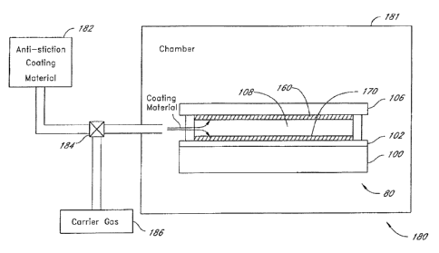
Figure 14 illustrates a protective coating system for an interferometric light
modulating
device 80 according to one embodiment of the invention. Referring to Figure
14, the system 180
comprises a chamber 181, a coating material container 182, a valve 184, and a
carrier gas
reservoir 186. A person skilled in the art will appreciate that the system 180
is only exemplary
and other coating systems, which can exclude some of the elements or layers of
the system 180
and/or include additional elements, can be used. In one embodiment, the system
180 can perform
a protective coating for the fabricated package as shown in Figures 12A, 12B
and 12C.
The valve 184 controls feeding the coating material into the chamber 181. In
one
embodiment, the valve 184 is controlled by a computing device. In one
embodiment, the valve
184 can be any suitable valve for this protective coating process. In another
embodiment, the
valve 184 can be used to properly mix and time the Garner gas with the an
etchant gas, such as
XeFz.
The container 182 contains protective coating material. In various
embodiments, as
discussed above, an example of a protective coating can include, but is not
limited to, the
following: a self aligning (or self assembling) monolayer such as OTS,
dichlorodimethylsilane,
etc.; other polymeric materials such as teflon, polystyrene, etc.; or other
inorganic materials such
as graphite, DLC, etc. In another embodiment, the coating material includes
any protective
material which does not significantly adversely affect the optical responses
or characteristics of
the optical cavity 108, such as the optical responses and/or characteristics
of layers 102 or 106. In
a preferred embodiment, the protective coating material comprises a self
assembling monolayer
with a relatively low melting or vaporization point. This can allow the
protective coating to be
regenerated after a device containing the interferometric modulator device has
been assembled at
relatively low temperatures.
In one embodiment, the carrier gas reservoir 186 contains a carrier gas such
as nitrogen
(N2) or argon, which is used to transport the protective material to the
chamber 181 by a known
pumping mechanism. In another embodiment, the carrier gas can incorporate
other types of getter
material or chemistries as long as the performance of the interferometric
light modulating device
-20-
CA 02517109 2005-08-25
80 is not significantly adversely affected. In another embodiment, the carrier
gas can be
integrated into the chemistry of the release etchant gas of XeFz.
Figure I S is an exemplary flowchart describing a protective coating process
according to
one embodiment of the invention. One of skill in the art will appreciate that
depending on the
embodiments, additional steps can be added, others removed, or the order of
the steps changed.
Figure 15, demonstrates the protective coating procedure according to
embodiments of invention
and as shown in Figures 8-13.
Protective coating material is provided in step 90. The interferometric light
modulating
device 80, whose surface(s), such as layers 102 and/or 106, will be coated, is
placed in the
chamber 181 at step 92. A protective coating is applied on the surfaces to be
coated in step 94. In
one embodiment, the surface of layers 102 and/or 106, such as a minor surface
or an insulator
surface, can be heated so that water vapor existing on the surfaces to be
coated is removed before
the protective coating is performed. In one embodiment, the insulating
sublayer 130 is not
provided and the protective coating is formed on the surface of the primary
mirror sublayer 120
(depicted in Figure 9). In another embodiment, the protective coating is
formed on the surface of
the secondary mirror sublayer 140 (depicted in Figure 9). In another
embodiment, the protective
coating is formed on the surfaces of the insulating sublayer I30 and secondary
mirror sublayer
140 (depicted in Figure 9).
In one embodiment of the protective coating process, the protective coating is
formed
during an interferometric light modulating device fabrication process. For
example, the protective
coating can be incorporated into a "release" process. In the release process,
a sacrificial layer 175
(depicted in Figure 12C) of the interferometric light modulating device 80 is
etched away with the
use of a gas, for example, XeF2. In one embodiment, a mixture of the
protective coating material
and XeF2 can be pumped into the chamber 181. In another embodiment, the
protective coating
can be applied after the XeF2 etching is complete. Typically, the release
process is performed by
a MEMS etching system, for example, X3 Series Xetch available from XACIX, USA,
and MEMS
ETCHER available from Penta Vacuum, Singapore.
In another embodiment of the protective coating process, the protective
coating is uniform
in its thickness. In another embodiment, the thickness of the protective
coating is not uniform.
Generally, a protective coating such as a self aligned monolayer is a thin
film coating and thus it
does not significantly affect the optical characteristics (or responses) of
the layers 102 or 106,
including mirrors 120 and 140 (depicted in Figure 9), even if the protective
coating is not
uniform.
In one embodiment, the protective coating is performed using a process
disclosed in, for
example, "Dichlorodimethylsilane as an Anti-Stiction Monolayer for MEMS,"
Journal of
Microelectromechanical Systems, Vol. 10, No. 1, March 2001 and U.S. Patent No.
6,335,224. In
another embodiment, the protective coating is performed using a deposition
process, such as
-21-
CA 02517109 2005-08-25
chemical vapor deposition or a physical vapor deposition. In still another
embodiment, any
suitable protective coating method on mirror or insulator surfaces, either
known or developed in
the future, can be used. The protective coating process is then completed in
step 96 and the
interferometric light modulating device 80 is removed from the chamber 181 in
step 98.
Figure 16 is a flowchart describing a method for applying a protective coating
for an
interferometric light modulating device according to one embodiment of the
invention. This
Figure illustrates another method for reducing attractive forces between
layers within a light
modulating device. In accordance with this method, the interferometric light
modulating devices
described in the instant application can be fabricated, including the devices
described with
reference to Figures 8-13. In this method, a transmissive element is provided
in step 200. The
transmissive element can be provided by layering a transmissive layer upon a
substrate. This
transmissive element can be, for example, the entire fixed transmissive
element 102 or any of its
sublayers, such as the primary mirror sublayer (transmissive sublayer) 120,
the insulating sublayer
130, or electrode sublayer 110 depicted in Figure 9. A reflective element is
provided in step 210.
The reflective element can be provided by forming a thin film stack over the
transmissive
element. This reflective element can be, for example, the moveable reflective
layer 106 or any of
its sublayers, such as the secondary mirror sublayer 140 or the electrode
sublayer 150 depicted in
Figure 9. A protective coating is then provided in step 220, wherein the
protective coating is
located between at least a portion of the reflective layer and the
transmissive layer. The protective
coating can be provided as described herein with reference to Figures 12-15. A
person skilled in
the art will appreciate that the method depicted in Figure 16 is only
exemplary and other coating
methods, which can exclude some of the elements or steps in the depicted
method and/or include
additional elements, layers, or steps, can be used.
For example, in another embodiment, the reflective element can be provided
before the
transmissive element is provided. Also, in other embodiments, the protective
coating is provided
after either the reflective element or the transmissive element is provided.
Also, in other
embodiments, covering elements, such as a sacrificial layer, can be applied to
portions of the
interferometric light modulating device where a protective coating is not
desired. Then, if
desired, after the protective coating is provided, other elements may make
contact with the coated
covering element(s), thereby providing a protective coating by transfer
contact. The covering
elements and/or sacrificial layers can then be etched. In other embodiments, a
sacrificial layer is
provided between the reflective element and the transmissive element and the
sacrificial layer is
then etched prior to providing the protective coating. In other embodiments,
the transmissive
element and reflective element are packaged into an interferometric light
modulating device
package, such as one depicted in Figures 13A and 13B, prior to providing the
protective coating.
In other embodiments the protective coating is provided prior to the
packaging.
-22-
CA 02517109 2005-08-25
Regeneration of~the Protective Coating
Figure 17 shows a simplified and enlarged side-view of another embodiment of a
transmissive element or layer 102 that can be used in a MEMS configuration.
The transmissive
element has a protective coating, e.g., monolayer, 908 deposited over an
insulator layer 904. The
S insulator layer 904 is on a transmissive layer 902 which is on the substrate
900. There can be an
electrode layer, e.g., as shown in Figure 9, between layer 902 and the
substrate 900. The
insulating layer 904, can be formed, for example, by oxidizing, if aluminum is
being used, in an
oxygen plasma; thus, forming a thin Iayer of aluminum oxide.
Figure 18A is a side-view illustrating an embodiment of a package structure
340 for an
interferometric modulator array that can contain the transmissive element 102
depicted in Figure
17. Similar to the structures described above, the package structure 340
comprises an
interferometric modulator array 342 formed on a substantially transparent
substrate 344, such as
glass, and a backplate cover or "cap" 346 that encloses the array. The package
structure 340 can
further have a seal 348 formed or applied between facing surfaces of the
backplate 346 and the
substrate 344. In one embodiment, the primary seal 348 is a non-hermetic seal,
such as a
conventional epoxy-based adhesive. The various packaging systems described
above, as well as
other systems, can also be employed. Unlike the packaging systems described
above, the device
in Figure 18A further contains an optional heater 350, which can be used, as
described in more
detail below, to regenerate the protective coating.
Figure 18B is a plan-view illustrating the package structure 340 of Figure
18A. As
illustrated in Figure 18B, a plurality of conductive leads 352 (partially
shown) can be located on
the substrate 344 and configured to provide an electrical connection of a
driver circuit (not shown)
to the elements of the interferometric modulator array 342. The package
structure 340 can
include conductive leads 352 formed on more than one side of the substrate
344, and the
conductive leads are only illustrated on one side of the substrate and in the
configuration shown
for convenience.
The driver circuit is configured to control operation of the elements of the
interferometric
modulator array 342. As will be appreciated by one of skill in the art, the
conductive leads 352
can be positioned on the substrate 344 in a plurality of configurations and
the configuration
illustrated is exemplary in nature. In some embodiments the driver circuit is
used to control the
heater. In other embodiments, a separate device or element is used to control
the heater.
As will be appreciated by one of skill in the art, the driver circuit can be
located in various
areas of the package. In some embodiments, the driver circuit 353 is located
on the substrate, as
shown in Figure 18C. In this embodiment, the driver circuit can readily be
used to control the
heater, especially if the heater is on the substrate. As will be appreciated
by one of skill in the art,
in some embodiments, the heater is controlled through a device other than the
driver circuit. For
example, in embodiments in which the heater or heater leads are off of the
substrate, other
-23-
CA 02517109 2005-08-25
discrete components can be used to control the heater. For example, a power
transistor can be
used to control the heater. Given the present disclosure, one of skill in the
art will readily be able
to identify alternative means for powering or controlling the heater.
While the protective coatings discussed above have many possible advantages,
it has been
realized that during the operation of the interferometric modulator elements,
the protective coating
160, 170, or 908 may be rubbed or chipped off due to repeated contact from the
transmissive
element and the reflective element. The rubbing or chipping may or may not be
uniform over the
surface of the coating. The protective coating may flake away from the
insulator layer over a
period of time. Thus, it can be advantageous to repair this protective coating
at various times
throughout the life of the device. The following discloses various methods for
how the protective
coatings can be regenerated.
One embodiment of a method of regenerating or redistributing a protective
coating (e.g.,
self aligned monolayer) such as the shown protective coatings 908, 170, or 160
comprises
elevating the temperature of the protective coating 908, 170, or 160 to a
temperature at which the
protective coating material changes from a solid to a fluid, a vapor, or has
dramatically increased
vapor pressure such that the protective coating material is redistributed over
the layer it was
initially coating in a substantially uniform configuration. This allows the
protective coating to be
repaired and regenerated, even if it is still contained within a package
(e.g., Figures 13A, 13B,
18A, or 18B). This can be achieved through various devices. For example, an
optional heater
350 can be included in the package, as shown in Figure 18A.
Figure 18D depicts one embodiment of the method. First 300, one provides an
interferometric modulator device with a protective coating, preferably a
coating that has been
damaged or is suspected of having been damaged. Next, 310, one raises the
temperature of the
material of the protective coating so that the protective coating can
redistribute itself across a
surface. The protective coating material that is heated can either be the
material of the protective
coating itself (i.e., the coating on the reflective or transmissive elements)
or it can be from a
reservoir of protective coating material. Once the temperature has been
elevated for a period of
time to allow for redistribution of the material of the protective coating,
the device is allowed to
cool 320, which allows the protective coating to be solidified; thus,
regenerating the protective
coating. As will be appreciated by one of skill in the art, the method
depicted in Figure 18D can
be performed after the method depicted in Figures 15 and 16 or even during the
earlier procedure,
if it is helpful in initially establishing a monolayer.
As will be appreciated by one of skill in the art, elevating a temperature in
a device can be
measured in various ways, for example, at the temperature of the heating
element, or the
temperature at some point of the device to be heated. When an upper limit of
temperature is
discussed, it is generally in regard to the temperature of the item to be
heated, rather than the
heating element itself. One of skill in the art will recognize that the
heating element itself can be
-24-
CA 02517109 2005-08-25
heated to substantially higher temperatures in some embodiments than can the
device generally.
In a preferred embodiment, one obtains the desired amount of heat by running a
known current for
a known time through a particular heater. Given the present disclosure, the
current and time can
be determined through routine experimentation.
In some aspects, the invention is the use of a material as a protective
coating that can
allow the regeneration of the protective coating after the device is
assembled. Thus, in one
embodiment, protective coatings that are solid primarily at relatively low
temperatures and exhibit
relatively high volatility at elevated temperatures, and thus can be
redistributed in a system upon
heating, are contemplated. For example, protective coating materials that can
redistribute
themselves when heated above 22-50, 50-85, 85-100, 100-250, 100-110, 110-120,
120-150, 150-
200, 200-225, 225-250 °C, or more, can be used to make a device with a
protective coating with
regenerarive capabilities. As will be appreciated by one of skill in the art,
protective coatings with
higher stability at the lower temperatures can be advantageous for typical
working conditions, as
the protective coating should maintain a relatively solid form during typical
use of the device.
Various protective coatings have been discussed above. In a preferred
embodiment, the
material for the protective coatings can form a self assembled monolayer
(SAMs). Preferably, the
material, while solid under standard operation conditions, is readily melted
or vaporized upon the
addition of energy, such as heat. Thus, especially preferred are materials
that form SAMs, that
can be dissociated and regenerated at temperatures, and that will not damage
the elements of the
interferometric modulator device, the package, and/or the device containing
these items.
Exemplary materials for the regenerating protective coatings include, for
example, self aligning
monolayers, such as polytetrafluoroethylene (PTFE) and
octadecyltrichlorosilane (OTS).
Materials further include, for example, a long-chain aliphatic halogenated
polar
compound, such as a perfluoroalkanoic acid of the general formula
F3C(CFz)xCOOH, where X is
preferably 10 or more (e.g., perfluorodecanoic carboxylic acid), for example
10, 12, 14, 16 or 18.
The COOH moiety provides a good "anchor" to the surface of the transmissive or
reflective
element, while the free end or remainder of each molecule provides low surface
energy which
discourages sticking of the two elements. The attachment of the COOH moiety
can be enhanced
by appropriate pretreatment of the surfaces of the reflective or transmissive
layers. As discussed
herein, these molecules are selected on being able to form a stable protective
coating under typical
operating conditions, but by being sufficiently volatile when heated so as to
allow movement and
regeneration of the protective coating. One of skill in the art, given the
present disclosure will
recognize how to select or modify such a monolayer. For example, the number of
carbons in the
long chain or the number of double bonds in the long chain can alter the
stability of the protective
coating created. Additionally, additive can be added to further adjust the
melting point of the
protective coating.
-25-
CA 02517109 2005-08-25
In some embodiments, multiple types of protective coating materials can be
used at once.
In some embodiments, an initial protective coating is established that is
difficult to regenerate
(e.g., TeflonTM) and a second type of protective coating material is also
added to the device that is
readily regenerated. In some embodiments, the second type of protective
coating material is
selected so that it will preferably bind to any gaps in the TeflonTM coating,
thus reestablishing a
complete protective coating. In some embodiments, the "underneath" coating can
be chosen to
adjust other parameters, such as adhesion and temperature dependence.
While the embodiments discussed herein concentrate on methods and compositions
that
use sources of heat that are internal to a package, in some embodiments the
heat or energy source
can be located externally to the package 85. Thus, in some embodiments, an
external heat source
can heat either the entire package or a part of the device (e.g., just the
reflective and/or
transmissive elements). This can be done in a variety of ways, for example,
using radiation, such
as a laser, or heating the atmosphere around the device. The heat can be
administered through the
substrate 344 or e.g., through the backplate 346. The heat can be administered
via radiation,
conduction, or convection.
Figure 19 is a plan-view illustrating another embodiment of a system 354 for
regenerating
a protective coating formed on the surfaces of an interferometric modulator
array 342. The
system illustrated in Figure 19 comprises a heater, e.g., a heater element 355
positioned proximal
to the interferometric modulator array 342. The heater element 355 can be
fabricated by
photolithographic patterning of one or more metallic layers deposited during
the fabrication of the
interferometric modulator structure. The heater element 355 is configured to
emit heat in
response to current generated by the application of a predefined current at
conductive leads 356A
and 356B, wherein the amount of heat emitted by the heater element 355 is
sufficient to raise the
temperature of the protective coating (e.g., self aligned monolayer) such that
the coating is
redistributed over the conductor layer.
Application of a current to the conductive leads 356A and 356B can be
controlled, for
example, by the driver circuit (not shown) which is also configured to control
operation of the
elements of the interferometric modulator array 342 via conductive leads 352.
The driver circuit
can be configured to apply a predefined current to the heater element 355 on a
fixed periodic basis
during the lifetime of the interferometric modulator array 342 when
implemented in an electronic
device. In other embodiments, application of a predefined voltage is used. As
will be appreciated
by one of skill in the art, the driver circuit itself can be located on the
glass. However, in some
embodiments, such as when the heater is not on the glass, the driver circuit
does not have to be on
the glass. In some embodiments, the driver circuit is not used to control the
heater and another
source of current/voltage is used.
In one embodiment, the heater element 355 is positioned on the substrate 344.
In other
embodiments, multiple heater elements can be implemented, for example,
proximal to each edge
-26-
CA 02517109 2005-08-25
of the interferometric modulator array 342. As will be appreciated by those
skilled in the
technology, the configuration of the heater element 355 is not limited to that
shown or described,
and additional configurations are contemplated. The actual configuration and
placement of the
heaters will vary depending upon the desired application, and one of skill in
the art, in light of the
present disclosure, will be able to determine the appropriate placement and
configuration. For
example, the amount of space available, the proximity of the heating element
to other heat
sensitive devices, the level of heat required to substantially vaporize or
regenerate the protective
coating, the volatility of the protective coating material to heat, the
composition and resistance of
the heating element, and the composition of the substrate, to name a few
factors.
The term "heater," "heater device", "heater element," and other similar terms
are
interchangeable, where appropriate. Generally, "heater element" denotes the
actual substance that
is heated by electrical current or other means, while the heater can denote a
more general concept
of either an entire heating device or the element itself.
In another embodiment, the heater is not located on the substrate but
elsewhere in the
package. For example, the heater can be located on the backplate or cap 346.
For example, in
one embodiment, item 350 in Figure 18A is a heater; thus, the heater can be
attached to the
backplate in some embodiments.
As will be appreciated by one of skill in the art, the amount of heat required
and duration
of the application of the heat can be determined in a variety of ways. For
example, in a given
package, containing a damaged protective coating (which can be damaged on
purpose for the
purpose of testing) an amount of heat is applied to the device and the device
allowed to cool.
Following this, the surface and conformity of the protective coating can be
examined, either
functionally, or directly, e.g., via a microscope. This process can be
repeated, either in the same
or different devices, to determine the duration and amount of current required
to generate enough
heat for a particular heater in a particular package to sufficiently
regenerate a protective coating.
Various amounts of regeneration are contemplated, for example 1-10, 10-20, 20-
30, 30-40, 40-50,
50-60, 60-70, 70-80, 80-90, 90-99, and 99-100 percent regeneration of the
surface returned to its
original covered state. In some embodiments, a maximal current for a maximal
duration is used.
In a preferred embodiment, data from the above can be used to create a heating
protocol where a
predetermined current is run through the heating device for a predetermined
time to regenerate the
layer. In a preferred embodiment, no verification of the integrity of the
layer is required.
In some embodiments, it can be useful to have an additional reservoir of the
material of
the protective coating available in the package. This can be particularly
useful in situations where
the protective coating is a monolayer. In some embodiments, both the exposed
surface of the
reflective layer and the exposed surface of the transmissive layer are coated
with the protective
coating. In some embodiments, there is a reservoir of the protective coating
material in the
package, which is in addition to the amount that is already on either or both
of the transmissive
-27-
CA 02517109 2005-08-25
and reflective layers. In some embodiments the reservoir is more than a
monolayer thick. The
reservoir can be distributed throughout the package so that excess protective
coating material is
available throughout the package and surrounding the interferometric modulator
device array.
The reservoir can be positioned on top of or near the heating element. Thus,
in some
embodiments, a very low level of heat is all that needs to be applied in order
to have the
protective coating material of the reservoir capable of redistributing itself.
In some embodiments,
the reservoir is simply the presence of more protective coating material than
is required to coat
one surface of either the transmissive or reflective layers.
As will be appreciated by one of skill in the art, in embodiments that use a
reservoir, any
structure in the package or interferometric modulator device can be used as a
surface for adding a
reservoir of the packaging material, including various posts, supports, and
packaging surfaces. As
will be appreciated by one of skill in the art, the addition of the protective
coating by wafting it
into the package or across an interferometric modulator device can naturally
result in excess
protective coating material in the package or on the interferometric modulator
device, thus
establishing a reservoir. In embodiments in which the protective coating has
been added through
wafting of the protective coating material though a hole in the package, the
protective coating
material can be located throughout the various surfaces of the package. In
embodiments in which
the protective coating is wafted onto the interferometric modulator device
before the device is
enclosed within the package, only the interferometric modulator device can be
coated with the
protective coating. As will be appreciated by one of skill in the art, not
every type of protective
coating may adhere to every surface available. The type of protective coating
material can be
selected based on the previously mentioned characteristics, as well as where
and how much of the
protective coating is desired in the final device. In some embodiments,
additional protective
material is added to the device after it has been used. In some embodiments,
the establishment of
the protective coating is done before the first use of the device for its
intended purpose. In other
embodiments, the heating or heaters described herein is employed when the
protective coating is
first established, to help establish a uniform coating of the protective
coating.
In some embodiments, the regenerative components and methods are used with an
interferometric modulator device with a getter or desiccant. As will be
appreciated by one of skill
in the art, the temperature of the getter generally should not be raised to
the point that water that
has been absorbed is lost. This can be achieved by thermally isolating the
getter from the heater
system, or maintaining the temperature of the heater beneath a certain
temperature. In some
embodiments, a desiccant or getter is not employed when a heater is employed.
In some embodiments, only one protective coating is required between the
transmissive
and reflective layers. Thus, when more than one surface area is covered, the
additional material
can be considered a reservoir. As will be appreciated by one of skill in the
art, where the reservoir
is the complementary layer, heating of the device may result in movement of
protective coating
-28-
CA 02517109 2005-08-25
from one layer to the other layer. It is permissible that one layer loose
protective coating so that
the other layer is able to regenerate its protective coating.
As will be appreciated by one of skill in the art, in some embodiments, the
protective
coating is not "completely" regenerated. Rather, in some embodiments, the
section of the coating
that has been damaged is regenerated while another section of the coating is
exposed. This can
occur without detrimental impact to the operation of the device when the
section from which the
protective coating material is taken is from a part of the layer that does not
contact the other layer.
This could include, for example, the section of the portion of the reflective
layer 14b that is
located between the supports 18 and where the reflective layer 14b contacts
the transmissive layer
16b. One of skill in the art will appreciate that, to some extent, such a
repositioning of the
material of the protective coating will occur due to the fact that the
location of the damage to the
protective coating will be, for example, where contact occurs between the two
layers, thus
creating a relatively low concentration of the material there, and
redistribution of the protective
coating, while random, will result in an increase in protective coating
material at the damaged site
and a reduced concentration at the undamaged site. This can be readily
achieved by using self
assembled monolayers, the molecules of which will redistribute themselves
across a layer. Thus,
in some embodiments, only the contact zone (the area of one element that
contacts the other
element) of the protective coating is regenerated or partially regenerated.
Another embodiment of the system 362 for regenerating the protective coating
of the
interferometric modulator array 342 is shown in Figure 20A. In this
embodiment, there are
conductive leads 352 that can be repurposed so as to emit heat sufficient to
redistribute the
protective coating in response to application of a predefined voltage. In one
embodiment, an
element or layer already in the interferometric modulator device is repurposed
as a heater.
Typically, the conductive leads extend from the driver circuit, through the
interferometric
modulator array, and terminate open-ended at the far-side of the array. In
some embodiments, a
plurality of these conductive leads can be routed back, or "looped" to the
driver circuit around the
periphery of the array. During normal operation, the looped leads are isolated
from ground
potential by transistor switches (for example) inside the driver circuit. When
redistribution of the
protective coating is desired, the transistor switches are activated to short
the looped leads to
ground potential, and the application of a predefined current or voltage will
cause one or more of
the looped leads to emit sufficient heat to redistribute the protective
coating of the interferometric
modulator array 342. In some embodiments, a current limiting resistor is in
the loop between the
lead and ground.
In one embodiment, the heat generating current is looped through the
transmissive layer.
In a preferred embodiment, the heat generating current is looped through a
circuit that has a
relatively high resistance so that a desired amount of heat can be generated.
As mentioned above,
the transmissive layer can comprise a relatively high resistance material,
such as chrome. In
-29-
CA 02517109 2005-08-25
embodiments in which the protective coating is attached to the transmissive
layer, either directly
or indirectly, this can be advantageous, as heat will be generated on the
surface that requires
additional or redistribution of the protective material of the coating. In
another embodiment, the
heat generating current is looped through another conductive layer that has a
relatively high
S resistance (such as a layer having chrome or nickel in it), such as a
mechanical layer (or moveable
layer) 34 in the device.
As will be appreciated by one of skill in the art, in some embodiments, any
substance or
part of the interferometric modulator device or package that will emit heat
when a current is run
through it can be used. As will be appreciated by one of skill in the art, the
interferometric
modulator device need not be operational during the regeneration step,
therefore even devices or
elements that might normally be required for the operation of the
interferometric modulator
device can be used as heaters. As will be appreciated by one of skill in the
art, it can be desirable
for there to be a relatively large amount of space above the surface that is
to be repaired, as it can
allow a more efficient regenerative process to occur. Thus, in some
embodiments, the reflective
1 S and transmissive elements are positioned relatively far away from one
another during the
regenerative process.
In some embodiments, the isolation switches for the above embodiment can be
implemented on the substrate as MEMS switches 365 as illustrated in Figure
20A, wherein the
MEMS switches are coupled to a common ground connection in the driver or else-
where. Figure
20B is a perspective-view illustrating an exemplary MEMS switch 366. The MEMS
switch 366
comprises a substrate 370 having a primary conductor layer 372 formed thereon.
An insulator
layer can be formed on the primary conductor layer 372. However, the insulator
layer is not
illustrated in Figure 20B for convenience, and reference to the primary
conductor layer 372
should be understood to comprising the combination of the conductor layer 372
and an insulator
layer formed thereon.
The MEMS switch 366 further comprises a secondary conductor layer 374 which is
configured to deform toward the primary conductor layer 372 in response to
application of a
voltage, similar to the reflective layer (or conductor layer) 14b illustrated
in Figure 1. The MEMS
switch 366 can be fabricated, for example, as described in detail in U.S.
Patent No. 5,835,255 in
reference to Figures 26A-K. The MEMS switch 366 also includes one or more
switch conductors
376 formed on the primary conductor layer 372. During operation, the secondary
conductor layer
374 deforms toward primary conductor layer 372 in response to application of a
voltage V (see
Figure 1, for example). When the secondary conductor layer 374 contacts the
switch conductors
376, the MEMS switch 366 allows current to flow between conductors 376. Thus,
the MEMS
switch 366 can be actuated in response application of a predefined voltage to
the primary and
secondary conductors 372 and 374.
-30-
CA 02517109 2005-08-25
In some embodiments, the heater or heater element is positioned relatively
close to the
reflective layer. This can be achieved in a variety of ways. For example, as
discussed above, a
heater can be located on the backplate of a package.
Figure 21A is another embodiment in which the heater is placed relatively
close to the
reflective layer. Figure 21A is a side-view illustration of another embodiment
of a system 380 for
regenerating a self aligning monolayer for an interferometric modulator array.
Similar to the
interferometric modulator elements illustrated in Figure 1, the system 80
comprises a transmissive
layer 502 formed on the substrate 500, and a reflective layer 506 supported by
the insulating
supports 504. An insulator layer 382, similar to insulator layer 904 (Figure
17), is formed on the
transmissive layer 502, and a protective coating, such as a self aligning
monolayer, 384 is also
present (similar to the protective coating 908 in Figure 17), having been
formed on the insulator
layer 382. In certain embodiments, the protective coating is distributed over
a plurality of
surfaces and is not limited to formation on top of the insulation layer 382.
As illustrated in Figure 21A, the system 380 can further comprise one or more
posts 386
formed on the insulator layer 384 between adjacent reflective layers 506 (see
Figure 21B). The
posts 386 extend away from the insulator layer 384 and can extend beyond the
height of the
reflective layer 506. The posts 386 are configured to support a heater grid
388 or individual
heating elements. The heater grid 388 is configured to emit heat in response
to a predefined
voltage or current. The emitted heat is sufficient to raise the temperature of
the protective coating
such that the protective coating or additional protective coating is
redistributed substantially
uniformly over the insulator layer 382 or whichever layer the protective
coating is covering. In
one embodiment, the protective coating is redistributed without heating the
layer 384 to any great
extent. For example, an additional amount of protective coating material can
be located on the
heater grid; and thus, only the heater grid need be heated to any significant
degree.
Figure 21B is a plan-view illustration of the system 380 of Figure 21A. The
tops of the
posts 386 are shown for illustration purposes only. The substrate 500 can
include conductive
leads (not shown) for connection between the heater grid 388 and a driver
circuit (not shown) for
the interferometric modulator array. The driver circuit is configured to
control application of a
current or voltage to the heater grid 388, thereby controlling the
regeneration of the protective
coating 384. As will be appreciated by one of skill in the art, the current
need not be provided by
the driver IC, and other sources of voltage/current can be used for these
heaters. When the heater
leads are off of the glass, one can readily supply voltage/current through
alternative
voltage/current sources.
As will be appreciated by one of skill in the art, in light of the present
disclosure, the
heater or heater grid 388, can be positioned at various levels. For example,
while the heater grid
388 is shown above the reflective layer or element 506, it can also be
positioned in the same plane
as the reflective layer or element, beneath, or partially beneath the
reflective layer or element 506.
-31-
CA 02517109 2005-08-25
Additionally, the position of the protective coating can be varied or a
protective coating can be
applied throughout the entire interferometric modulator device or the entire
package. As will be
appreciated by one of skill in the art, positioning the protective coating on
the reflective layer 506,
which is closer to the heater grid 388 in this embodiment, can allow for a
lower amount of heat
from the heater grid to be sufficient to redistribute the protective coating
across the layer.
In some embodiments, the various embodiments described above are combined. For
example, in some embodiments, multiple types of heaters are combined, or
multiple methods of
heating and regenerating the device are performed simultaneously. For example,
an external
source of heat can be applied at the same time an internal heater is being
used, which may allow
for a higher efficiency of regeneration to occur.
In some embodiments, a bus system, which is positioned above the reflective
element,
similar to what is shown in Figure 22, can be repurposed for heating of the
protective coating. In
this embodiment, the interferometric modulator device 600 is similar to other
interferometric
modulator devices (it has a cavity 660 and reflective and transmissive
layers), but it further has a
bus structure 671 that is located on top of the supports. The bus structure
can be repurposed as
described above (e.g., particular MEMS switches or transistors). One advantage
of this structure
is that the heater or heating element takes up no additional space from the
interferometric
modulator device; thus, there is no loss in resolution of the device.
Additionally, as the bus
structure 671 is located on top of the supports for the reflective layer,
additional supports do not
need to be added to the device to support the heater. A detailed description
of a bus structure and
how to make it is disclosed in U.S. Patent Application No: 10/644,312, filed
August 19, 2003.
The foregoing description details certain embodiments of the invention. It
will be
appreciated, however, that no matter how detailed the foregoing appears in
text, the invention can
be practiced in many ways. It should also be noted that the use of particular
terminology when
describing certain features or aspects of the invention should not be taken to
imply that the
terminology is being redefined herein to be restricted to including any
specific characteristics of
the features or aspects of the invention with which that terminology is
associated.
Figures 23A and 23B are system block diagrams illustrating an embodiment of a
display
device 2040. The display device 2040 can be, for example, a cellular or mobile
telephone.
However, the same components of display device 2040 or slight variations
thereof are also
illustrative of various types of display de vices such as televisions and
portable media players.
The display device 2040 includes a housing 2041, a display 2030, an antenna
2043, a
speaker 2045, an input device 2048, and a microphone 2046. The housing 2041 is
generally
formed from any of a variety of manufacturing processes as are well known to
those of skill in the
art, including injection molding, and vacuum forming. In addition, the housing
2041 may be
made from any of a variety of materials, including but not limited to plastic,
metal, glass, rubber,
and ceramic, or a combination thereof. In one embodiment the housing 2041
includes removable
-32-
CA 02517109 2005-08-25
portions (not shown) that may be interchanged with other removable portions of
different color,
or containing different logos, pictures, or symbols.
The display 2030 of exemplary display device 2040 may be any of a variety of
displays,
including a bi-stable display, as described herein. In other embodiments, the
display 2030
includes a flat-panel display, such as plasma, EL, OLED, STN LCD, or TFT LCD
as d escribed
above, or a non-flat-panel display, such as a CRT or other tube device, as is
well known to those
of skill in the art. However, for purposes of describing the present
embodiment, the display 2030
includes an interferometric modulator display, as described herein.
The components of one embodiment of exemplary display device 2040 are
schematically
illustrated in Figure 23B. The illustrated exemplary display device 2040
includes a housing 2041
and can include additional components at least partially enclosed therein. For
example, in one
embodiment, the exemplary display device 2040 includes a network interface
2027 that includes
an antenna 2043 which is coupled to a transceiver 2047. The transceiver 2047
is connected to the
processor 2021, which is connected to conditioning hardware 2052. The
conditioning hardware
2052 may be configured to condition a signal (e.g. filter a signal). The
conditioning hardware
2052 is connected to a speaker 2045 and a microphone 2046. The processor 2021
is also
connected to an input device 2048 and a driver controller 2029. The driver
controller 2029 is
coupled to a frame buffer 2028 and to the array driver 2022, which in turn is
coupled to a display
array 2030. A power supply 2050 provides power to all components as required
by the particular
exemplary display device 2040 design.
The network interface 2027 includes the antenna 2043 and the transceiver 2047
so that
the exemplary display device 2040 can communicate with one or more devices
over a network. In
one embodiment the network interface 2027 may also have some processing
capabilities to relieve
requirements of the processor 2021. The antenna 2043 is any antenna known to
those of skill in
the art for transmitting and receiving signals. In one embodiment, the antenna
transmits and
receives RF signals according to the IEEE 802.11 standard, including IEEE
802.11(a), (b), or (g).
In another embodiment, the antenna transmits and receives RF signals according
to the
BLUETOOTH standard. In the case of a cellular telephone, the antenna is
designed to receive
CDMA, GSM, AMPS or other known signals that are used to communicate within a
wireless cell
phone network. The transceiver 2047 pre-processes the signals received from
the antenna 2043
so that they may be received by and further manipulated by the processor 2021.
The transceiver
2047 also processes signals received from the processor 2021 so that they may
be transmitted
from the exemplary display device 2040 via the antenna 2043.
In an alternative embodiment, the transceiver 2047 can be replaced by a
receiver. In yet
another alternative embodiment, network interface 2027 can be replaced by an
image source,
which can store or generate image data to be sent to the processor 2021. For
example, the image
-33-
CA 02517109 2005-08-25
source can be a digital video disc (DVD) or a hard-disc drive that contains
image data, or a
software module that generates image data.
Processor 2021 generally controls the overall operation of the exemplary
display device
2040. The processor 2021 receives data, such as compressed image data from the
network
interface 2027 or an image source, and processes the data into raw image data
or into a format that
is readily processed into raw image data. The processor 2021 then sends the
processed data to the
driver controller 2029 or to frame buffer 2028 for storage. Raw data typically
refers to the
information that identifies the image characteristics at each location within
an image. For
example, such image characteristics can include color, saturation, and gray-
scale level.
In one embodiment, the processor 2021 includes a microcontroller, CPU, or
logic unit to
control operation of the exemplary display device 2040. Conditioning hardware
2052 generally
includes amplifiers and filters for transmitting signals to the speaker 2045,
and for receiving
signals from the microphone 2046. Conditioning hardware 2052 may be discrete
components
within the exemplary display device 2040, or may be incorporated within the
processor 2021 or
other components.
The driver controller 2029 takes the raw image data generated by the processor
2021
either directly from the processor 2021 or from the frame buffer 2028 and
reformats the raw
image data appropriately for high speed transmission to the array driver 2022.
Specifically, the
driver controller 2029 reformats the raw image data into a data flow having a
raster-like format,
such that it has a time order suitable for scanning across the display array
2030. Then the driver
controller 2029 sends the formatted information to the array driver 2022.
Although a driver
controller 2029, such as a LCD controller, is often associated with the system
processor 2021 as a
stand-alone Integrated Circuit (IC), such controllers may be implemented in
many ways. They
may be embedded in the processor 2021 as hardware, embedded in the processor
2021 as
software, or fully integrated in hardware with the array driver 2022.
Typically, the array driver 2022 receives the formatted information from the
driver
controller 2029 and reformats the video data into a parallel set of waveforrns
that are applied
many times per second to the hundreds and sometimes thousands of leads coming
from the
display's x-y matrix of pixels.
In one embodiment, the driver controller 2029, array driver 2022, and display
array 2030
are appropriate for any of the types of displays described herein. For
example, in one
embodiment, driver controller 2029 is a conventional display controller or a
bi-stable display
controller (e.g., an interferometric modulator controller). In another
embodiment, array driver
2022 is a conventional driver or a bi-stable display driver (e.g., an
interferometric modulator
display). In one embodiment, a driver controller 2029 is integrated with the
array driver 2022.
Such an embodiment is common in highly integrated systems such as cellular
phones, watches,
-34-
CA 02517109 2005-08-25
and other small area displays. In yet another embodiment, display array 2030
is a typical display
array or a bi-stable display array (e.g., a display including an array of
interferometric modulators).
The input device 2048 allows a user to control the operation of the exemplary
display
device 2040. In one embodiment, input device 2048 includes a keypad, such as a
QWERTY
S keyboard or a telephone keypad, a button, a switch, a touch-sensitive
screen, a pressure- or heat
sensitive membrane. In one embodiment, the microphone 2046 is an input device
for the
exemplary display device 2040. When the microphone 2046 is used to input data
to the device,
voice commands may be provided by a user for controlling operations of the
exemplary display
device 2040.
Power supply 2050 can include a variety of energy storage devices as are well
known in
the art. For example, in one embodiment, power supply 2050 is a rechargeable
battery, such as a
nickel-cadmium battery or a lithium ion battery. In another embodiment, power
supply 2050 is a
renewable energy source, a capacitor, or a solar cell, including a plastic
solar cell, and solar-cell
paint. In another embodiment, power supply 2050 is configured to receive power
from a wall
outlet.
In some implementations control programmability resides, as described above,
in a driver
controller which can be located in several places in the electronic display
system. In some cases
control programmability resides in the array driver 2022. Those of skill in
the art will recognize
that the above-described optimization may be implemented in any number of
hardware and/or
software components and in various configurations.
While the above detailed description has shown, described, and pointed out
novel features
of the invention as applied to various embodiments, it will be understood that
various omissions,
substitutions, and changes in the form and details of the device or process
illustrated may be made
by those skilled in the art without departing from the spirit of the
invention. As will be
recognized, the present invention may be embodied within a form that does not
provide all of the
features and benefits set forth herein, as some features may be used or
practiced separately from
others.
-35-