Note: Descriptions are shown in the official language in which they were submitted.
CA 02517579 2005-08-26
WO 03/073185 PCT/CA03/00245
Title: PREDICTIVE CONTROL SYSTEM AND METHOD
FIELD OF THE INVENTION
This invention relates to a control system and method and more
particularly to a control system and method that incorporates predictive
techniques for application to a digital switching system.
BACKGROUND OF THE INVENTION
Traditional power electronic control systems using switch-mode
principles are typically structured to accommodate the needs of an overall
system that include a power circuit (actuator), a power load (plant), and a
controller that controls the operation of the power circuit. Many of the
overall
system elements are non-linear, and possess numerous energy storage
elements. Conventional simulation software allows. designers to simulate the
operation of the overall system so hat a particular control system can be
verified for proper function prior to construction.. However, commercially
available simulation software does not take into account all real life effects
(e.g. switching delays, and/or interlock delays). Ignoring these effects can
substantially affect simulation results.
Further, controllers that are verified using such software cannot
be easily modified to take proper account of real life effects. For this
reason,
standardization of power electronic designs has been difficult to achieve.
Systems controller design has evolved to include pre-design capture and
simulation which validates the quality of the design before it is built.
However,
post production revisions to a controller designed using these kinds of pre-
design simulation techniques, is generally costly, time consuming and
unmanageable, leading to early design obsolescence.
SUMMARY OF THE INVENTION
The present inverition in one aspect provides a control system
for controlling the operation of a power circuit, the power circuit having N
binary switches for one of.providing power to and receiving power from a load
circuit, the various configurations of the N switches being represented by a
CA 02517579 2005-08-26
WO 03/073185 PCT/CA03/00245
_2_
finite state machine having up to 2N switch states, the present configuration
of
the N binary switches being associated with a present switch state and having
a plurality of next switch states according to state transition constraints of
the
finite state machine, the control system comprising:
(a) an acquisition module for .acquiring a set of operational
signals related. to the load circuit associated with the present
switch state;
(b) an embedded simulator coupled to the acquisition module
for estimating a set of estimated operational characteristics of
the load circuit based on the set of operational signals and the
present switch state;
(c) a next state contemplator coupled to the embedded
simulator for estimating a set of estimated operational
characteristics of the load circuit for each .of the plurality of next
switch states, for comparing and selecting the next switch state
having estimated operational characteristics that best meet a
first set of criteria, and for actuating the power circuit to change
the switch configuration of the N binary switches therein to the
switch configuration associated with the next selected switch
state of the plurality of next states.
The present invention in another aspect provides a method for
controlling the operation of a power circuit, ttie power circuit having N
binary
switches for one of providing power to and receiving power from a load
circuit,
the various configurations of the N switches being represented by a finite
state machine having up to 2N switch states, the present configuration of the
N binary switches being associated with a presenfi switch state and having a
plurality of next switch states according to state transition constraints of
the
finite state machine, the method comprising the steps:
(a) acquiring a set of operational signals related to the load
circuit;
CA 02517579 2005-08-26
WO 03/073185 PCT/CA03/00245
-3-
(b) estimating a set of estimated operational characteristics
based on the set of operational signals and on the present
switch state;
(c) comparing and selecting the next switch state having
estimated operational characteristics that best meet a first set of
criteria,
(d) changing the configuration of the N binary switches to. the
switch configuration associated with the selected next switch
state of the plurality of next switch states.
The present invention in another aspect provides a method for
determining the voltage provided by a power circuit having N switches in a
circuit configuration, where each switch includes a unidirectional current
element having a connected node that is coupled to a voltage source and an
opposite node, each switch having a present current direction, the method
comprising:
(a) for each switch that opens:
(i) determining the direction of the present current
direction with respect to a free-wheeling current path of
the unidirectional current element;
(ii) if the present current direction is positive with respect
to the free-wheeling current path, then the voltage at the
opposite node is a determined voltage and is equal to the
voltage at the connected node;
(iii) if the present current direction is negative with respect
to the free-wheeling current path, then the voltage at the
opposite node is an undetermined voltage; and
(b) combining the values of all determined voltages present at the
opposite nodes of each switch in accordance with the circuit
CA 02517579 2005-08-26
WO 03/073185 PCT/CA03/00245
., _t~_
configuration of the power circuit to form a vector representing the
voltage provided by the power circuit.
BRIEF DESCRIPTION OF THE DRAWINGS
In the accompanying drawings:
FIG. 1 is a block diagram of a control system according to the
present invention;
FIG. 2 is an example of a finite state transition diagram that can
be utilized by the control system of FIG. 1;
FIG. 3 is a time event diagram illustrating the steps executed by
the sequential processing event manager of the control system of FIG. 1;
FIG. 4 is a flowchart illustrating the steps taken by the control
system when controlling the load circuit of FIG. 1;
FIGS. 5A and 5A-1 show a block diagram of the control system
of FIG. 1 adapted for application to an induction motor;
FIG. 5B is a block diagram of the hardware platform that is used
to implement the control system of FIG. 1;
FIGS. 6A and 6B are schematic diagrams of the d and ~q axis
equivalent circuit representation of the induction motor of FIG. 5A-1;
FIG. 7A is a schematic diagram of a standard three-phase
voltage source inverter power circuit utilized within the control system of
FIG.
5;
FIG. 7B is a d-q space plane representation and associated
equation relations of the voltage of the power circuit of FIG. 7A;
FIG. 8 is a block diagram of the A/D system of the control
system of FIG. 5A;
FIG. 9 is a block diagram of the embedded simulator of FIG. 5A
showing a number of individual functional blocks;
FIG. 10 is a schematic diagram of a 3:2 current converter that is
used by the embedded simulator of FIG. 9;
CA 02517579 2005-08-26
WO 03/073185 PCT/CA03/00245
_5_
FIG. 11A is a schematic diagram of an equivalent circuit
representation of the induction motor of FIG. 5A-1 that illustrates the
magnetic
and other losses that occur during operation;
FIG. 11 B is a schematic diagram of the loss compensator of
FIG.9;
FIG. 12A is a schematic diagram of an equivalent circuit
representation of the induction motor of FIG. 5A-1 that illustrates . the
relationships between motor model components;
FIG. 12B is a schematic diagram showing the relationship of the
main voltage, current and inductance of the induction motor of FIG. 5A-1 as
well as illustrating the principle of the integration calculation that is
traditionally
required to obtain a value for the main flux linkage;
FIGS. 13A and 13B are schematic diagrams showing the
switching state transitions adopted by a single totem-pole configuration
having
a variable direction of current i;
FIG. 13C is a schematic diagram showing the power circuit
switches of FIG. 5A-1 in various configurations to illustrate how interlock
voltage rules can be. derived based on various transitions between switch
states;
FIG. 13D is a listing of interlock voltage rules for the power
circuit switches of FIG. 5A-1 that are derived in the manner illustrated in
FIG.
13C;
FIG. 13E is a schematic diagram of a switch having a free-
wheeling unidirectional current element connected in a first configuration;
FIG. 13F is a schematic diagram of a switch having a free-
wheeling unidirectional current element connected in a second configuration;
FIG. 13G is a schematic diagram of a combination of the switch
elements of FIGS. 13E and 13F;
FIG. 14A is a schematic diagram of the main flux
predictor/corrector of FIG. 9;
CA 02517579 2005-08-26
WO 03/073185 PCT/CA03/00245
-6-
FIG. 14B is a listing of calculation statements that illustrate how
the main flux predictor/corrector of FIG. 14A utilizes the interlock voltages
which are determined by the rules of FIG. 13D along with the voltages
determined by the rules of FIG. 7B to compensate for interlock delay;
FIGS. 15 and 15-1 show a schematic diagram of the motor
characteristic calculator of FIG. 9;
FIG. 16 is a schematic diagram of the Present State
Contemplator of FIG. 5A;
FIGS. 17A, 17B and 17C illustrate a first and second method of
deriving an ideal stator flux vector;
FIG. 18 is a schematic diagram of the ideal stator flux reference
calculator block of Next State Contemplator of FIG. 5A;
FIG. 19 is a schematic diagram of the next state choice predictor
block of Next State Contemplator of FIG. 5A;
FIGS. 20 and 20-1 show a schematic diagram of four next state
choice predictor blocks of the Next State Contemplator of FIG. 5A that
correspond to four Next States for a particular Present State as defined by
the
finite state machine of FIG. 2;
FIG. 21 is a schematic diagram illustrating the processes
executed by State Transition Constraints Module, Next State Choice Criteria
Module, and Next State Contemplator of FIG. 5A;
FIG. 22 is a schematic diagram'of logic circuitry associated with
Embedded Simulator and Sequential Processing Event Manager of FIG..SA;
FIG. 23 is an example of a severed finite state transition
diagram that can be utilized by the control system of FIG. 5A in the case of a
particular detected failure mode;
FIG. 24 is a schematic of a modified motor model for a
synchronous machine having field magnets, or wound field excitation coils;
CA 02517579 2005-08-26
WO 03/073185 PCT/CA03/00245
_7_
FIG. 25 is a schematic diagram of an arrangement of two (or
more) control systems of FIG. 5A configured to control torque or flux within a
multi-stator winding machine while providing current regulation;
FIG. 26 is a schematic of a modified motor model for a
synchronous reluctance motor having a salient magnetic reluctance
characteristic;
FIG. 27 is a schematic diagram illustrating the use of the control
system of the present invention to generate and manage DC bus power for a
DC link provided by a rotating system; and,
FIG. 25 is a schematic diagram illustrating the use of the control
system of the present invention to adjust the power delivered by a three-
phase grid source.
DETAILED DESCRIPTION OF THE INVENTION
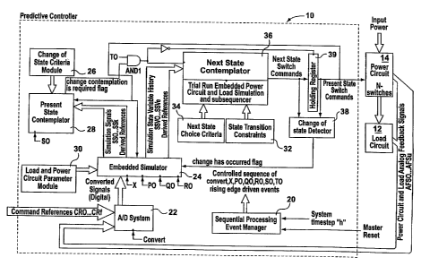
FIG. 1 is a block diagram illustrating a predictive control system
10, made in accordance with the invention. Control system 10 is designed to
control the operation of a switchable power circuit 14 associated with a load
circuit 12 using certain analog feedback variables from load circuit 12 as
well
as the switch configuration of power circuit 14 to achieve real time control
on
the basis of specified performance criterion. Control system 10 utilizes a
finite
state machine representation of the various switch states to model and predict
the behaviour of load circuit 12 based on various possible switch states of
power circuit 14 as switch state transitions are considered. Accordingly,
control system 10 simulates real time operation of load circuit 12 in order to
predictively select optimal switching states for power circuit 14.
Load circuit 12 can be any device or power process that
involves switch-mode power control, such as motor drives, uninterruptible
power supplies, corrosion protection systems, DC-DC converters, residential
AC inverters, fuel cell power conditioning systems, and plasma controllers.
Power circuit 14 is utilized to affect the operation of load circuit
12 using N binary switches (not shown). These discrete power switches are
connected into a power circuit configuration with a unique set of switch
states
CA 02517579 2005-08-26
WO 03/073185 PCT/CA03/00245
-$-
and characteristics (e.g. full bridge inverters; half-bridge inverters, open
collector, push-pull topologies etc.) The switches switch between on and off
states due to the requirement to control power efficiently (i.e. to minimize
losses) while simultaneously achieving some other control function (e.g.
torque control, temperature control, etc.) For each switch, two stable states
can be determined (i.e. "on" or "off'). In circuits with multiple (e.g. N)
switches,
up to 2N states can be defined. Accordingly, the switches of power circuit 14
are switched (i.e. modulated) by control system 10 through a binary data
instruction that can consist of up to N-bits, or up to 2N states.
Referring to FIGS. 1 and 2, an example finite state machine 50
and an associated set of transition constraints that is utilized by control
system 10 to model the configuration of the switches of power circuit 14 is
shown in FIG. 2. Finite state machine 50 represents an exemplary
hypothetical power circuit 14 with three binary switches and accordingly with
eight possible stable switch states (i.e. states VO to V7). States in which
two
complementary switches are closed are not allowed because they constitute a
short circuit of the DC bus in this particular example. The states where two
complementary switches are open, are allowed but only briefly during the
"interlock time". These states are not stable states and are handled and
accounted for by the interlock delay compensation technique to be described.
Each state of finite state machine 50 represents a "switch state" that can be
adopted by power circuit 14 and has a series of associated state variables
(i.e. operational characteristics of load circuit 12). The specific set of
transition
constraints embodied within the exemplary finite state machine 50 ensures
that each state has four possible transitions (including the transition of
remaining in the same state).
' At any time during the course of operation, power circuit 14 (i.e.
it's switches) will be in one specific switch state called "Present State":
Finite
state machine 50 defines a number of states into which power circuit 14 could
'transition to with one switch transition (i.e. a change of a single binary
switch),
or possible "Next States". Control system 10 determines the optimal Next
State for power circuit 14 on the basis of a number of constraints and sends
CA 02517579 2005-08-26
WO 03/073185 PCT/CA03/00245
- 9.-
power circuit 14 a binary instruction to cause power circuit 14 to enter into
that
optimal Next State.
It should be understood that control system 10 could utilize any
type of finite state machine and transition constraints to model a particular
set
of switch states for a particular power circuit 14. For example, one approach
would be to allow any change to occur in which case every state would have a
transition to every other state. However, such a rule would involve added
complexity and computational expense. Also, such a complex model may
result in potentially higher EMI due to an increase in switching events (i.e.
since the average switching frequency would have to be increased to achieve
similar performance levels as a more discriminating model). However, in
certain applications where the criterion for determining a change of state is
specialized, these additional switch choices may be advantageous. For
example, if complex magnetic saturation characteristics are prevalent in a
particular machine design and they are modeled accurately, one possible
criterion could be to minimize the di/dt in an efFort to minimize magnetic and
attendant audible noise and/or hysteresis/eddy current losses. In such a case,
in limiting the transitions to one-of-four choices it may still be possible to
satisfy this new criterion, but may result in the need for a "higher"
effective
20. switching frequency (i.e. average frequency at which the switch state S(x)
changes) to accomplish the same taste as compared to a rule which allowed
"all-of-eight" states to be chosen. The decision to allow all of eight or only
one
of four is contingent on the specific application requirements for control
system 10.
Referring back to FIG. 1, control system 10 includes a
Sequential Processing Event Manager 20, an optional A/D System 22
(explained further below), an Embedded Simulator 24, a Change of State
Criteria Module 26, a Present State Contemplator 28, a Parameter Module 30,
a State Transition Constraint Module 32, a Next State Choice Criteria Module
34, a Next State Contemplator 36, and a Change of State Detector 38.
Sequential Processing Event Manager 20 is coupled to all of the
functional blocks of control system 10 and coordinates the operation of each
block using a set of triggers (i.e. with convert, X, P0, Q0,_ R0, S0, and TO
CA 02517579 2005-08-26
WO 03/073185 PCT/CA03/00245
-10-
triggers as will be described). Control system 10 sequentially executes a
number of distinct processes over the course of a system time step "h". Each
distinct process involves the operation of one or more of the functional
blocks
of control system 10. Specifically, each system time step h, Sequential
Processing Event Manager 20 instructs: (1 ) A/D system 22 to acquire real
data from load circuit 12, (2) Embedded Simulator 24 to determine operational
characteristics of load circuit 12 based on measured characteristics of load
circuit 12 and the switch state of power circuit 14, (3) Present State
Contemplator 23 to consider whether switch state should be changed
(according to predefined change of state criteria) and if sothen (4) Next
State
Contemplator 36 to consider which Next State (i.e. of those switch states
reachable from the Present State) would be the optimal one (according to
predefined next state choice criteria stored in Next State Choice Criteria
Module 34).
A/D system 22 is a conventional A/D sampling converter that
samples and simultaneously converts analog real-world variables from the
load circuit 12 to discrete-time, representation. Conversion of analog real-
world variables associated with load circuit 12 'into discrete-time form is
achieved at a sample rate of 1/h. AID system 22 is provided with a convert
trigger that causes A/D system 22 to perform conversion of incoming
variables related to the load circuit 12. It should be understood that any
number of analog power circuit and load feedback variables may be acquired
and utilized within control system 10 for sampling and conversion by A/D
system 22 at sampling interval h.
In an alternative embodiment, the acquisition module or A/D
system 22 does not contain an A/D converter but rather comprises an
estimation module with a similar purpose to the A/D converter. In this case,
the real-world variables related to the load circuit 12 are estimated
accurately
enough to preclude the need for physical interface of real-world signals from
the load circuit as shown in Figures 1, 5A and 5B. With an estimation module,
the A/D system 22 no longer requires an external connection to the load
circuit 12, but can produce the necessary estimated operational signals
related. to the load circuit by accurately modeling the load circuit 12 and
CA 02517579 2005-08-26
WO 03/073185 PCT/CA03/00245
-11-
utilizing mathematical signal processing with appropriate initial conditions.
This capability offers significant advantage compared to other prior art
closed
loop control systems in that it allows the elimination of the AID converter
hardware typically required and produces the benefit of reduced cost and
circuit complexity.
Embedded Simulator 24 receives discrete-time representations
of analog "real-world" variables associated with load circuit 12 from A/D
System 22 as well as load and power circuit parameters and structural details
(e.g. component values and interconnections) from Parameter Module 30.
Embedded Simulator 24 also maintains a record of the switch configuration of
power circuit 14 (i.e. the present switch state). Using all of this
information,
Embedded Simulator 24 estimates essential operational characteristics of
load circuit 12 using discrete time simulation techniques. Embedded Simulator
24 is triggered by Sequential Processing Event Manager 20 (i.e, with X, P0,
Q0, and RO triggers as will be described) to execute various processing steps
within every h-cycle. Embedded Simulator 24 provides simulation signals and
other derived references to Present State Contemplator 28 and simulation
signals and other derived references to Next State Contemplator 36.
Change of State Criteria Module 26 stores and provides a set of
rules thafi determine the conditions under which a change of state is
contemplated (i.e. a change in switch configuration of power circuit 14 to
transition from Present State to a particular Next State which in the case of
the example shown in FIG. 2 is one switch transition away from the Present
State but which is generally, not necessarily, one switch transition away from
the Present State). It is important to note that Change of State Criteria
Module
26 only determines if a switch change should be considered, not that it will
actually occur.
Present State Contemplator 28 receives simulated and derived
motor model values from Embedded Simulator 24 and generates a binary
change of contemplation is required flag (i.e. "YES" or "NO") which is
forwarded back to Embedded Simulator 24 and to Next State Contemplator
36 every h-cycle. When suitably triggered by Sequential Processing Event
Manager 20 (i.e. by SO trigger as will be described), Present State
CA 02517579 2005-08-26
WO 03/073185 PCT/CA03/00245
-12-
Contemplator 28 uses the rules as stored i,n Change of State Criteria Module
26 along with the real-time and/or derived information from Embedded
Simulator 24 to determine whether a change of switch state should be
contemplated for a particular Present State. If so then Present State
Contemplator 28 provides a positive (i.e. "YES") change of contemplation is
required flag to Next State Contemplator 36.
Parameter Module 30 is utilized to provide Embedded Simulator
24 with the specific load circuit 12 and power circuit 14 parameters and
structural details that define the specific components of load circuit 12 and
power circuit 14 (e.g. inductor, capacitors, resistors and their values, as
well
as details on their interconnections and performance functionality). This
information is necessary for Embedded Simulator 24 to properly model load
circuit 12 and power circuit 14.
State Transition Constraints Module 32 contains data that
specifies the available transition vectors between the .various switch states
(e.g. the structure of finite state machine 50 of FIG. 2) adopted by the
switches of power circuit 14.
Next State Choice Criterion Module 34 contains Next State
Choice Criteria that constitutes a set of acceptance criteria and analysis
methods that are used to select an optimal Next State for transition from a
particular Present State. This information allows Next State Contemplator 36
to evaluate the expected performance of power circuit 14 and load circuit 12,
for each of the proposed Next States from a particular Present State.
Next State Contemplator 36 receives .motor model simulation
and derived results from Embedded Simulator 24 and the c h a n g a
contemplation is required flag from Present State Contemplator 28 and
provides a next state switch command to a holding register 39 which in turn
forwards the next state switch commands to power circuit 14. Next State
Contemplator 36 also provides the next state switch command to Change of
State Detector 38 which will then forward Next State information to Embedded
Simulator 24. When suitably triggered by Sequential Processing Event
Manager 20 (i.e. by TO trigger as will be described); Next State Contemplator
CA 02517579 2005-08-26
WO 03/073185 PCT/CA03/00245
-13-
36 determines the Next State that best meets the Next State' Choice Criteria
as stored in the Next State Choice Criteria Module 34. This is achieved by,
based on the Present State, determining the available Next State as defined
by State Transition Constraints Module 32 (e.g. the finite state machine 50),
simulating the result of adopting each possible Next State, and calculating
which result is the best result in view of the Next State Choice Criteria.
For each possible Next State, Next State Contemplator 36
conducts a number of "trial run" simulations with system time step "h" for
each possible Next State to produce a prediction of the conditions associated
with each. As previously mentioned, it is possible that one possible state
transition action is to simply remain in the same state. Accordingly, a "trial
run"
simulation with system time step "h" is also conducted for the Present State.
Using the Next State Choice Criteria contained in Next State Criteria Module
34, the results of each "trial run" is compared to determine the "best" choice
transition, which is then actuated in real time as the new Present State
switch
commands provided to power circuit 14 through holding register 39.
As mentioned, Change of State Detector 38 is utilized to detect
when a change of state has occurred (i.e. when the Next State is ,determined
to be different from the Present State) and to send a positive (i.e. "YES")
change has occurred flag to Embedded Simulator 24 when it has. This
allows Embedded Simulator 24 to execute subsequent internal process steps
to maintain proper simulation of the operational characteristics of load
circuit
12 (e.g. compensation of switch interlock delays etc.)
Accordingly, control system 10 utilizes a simulation model (i.e.
constructed by Embedded Simulator 24) of power circuit 14 and load circuit
12 to select an optimal Next State for the discrete switches of power circuit
14
based on the Present State and on certain Change of State criterion (i.e.
maintained in Change of State Criteria Module 26) used in conjunction with
Next State Choice criterion (i.e. maintained in Next State Choice Criteria
Module 34). The finite state machine 50 stored within State Transition
Constraints Module 32 defines a series of Next States for each Present State
that are evaluated by control system 10 to ensure optimal switch changes are
selected.
CA 02517579 2005-08-26
WO 03/073185 PCT/CA03/00245
- 14 --
Specifically, Present State Contemplator 28 determines based
on the Present State and the Change of State Criteria Module 26 whether
Next State Contemplator 36 should consider a change of state. If so, then the
change contemplation is required flag is. provided to Next State
Contemplator 36 that then in turn runs a series of "trial-runs" for the
various
potential Next States: Based on the Present State, Next State Choice Criteria
34 and real time analog feedback of variables in the power circuit 14 and load
circuit 12, Next State Contemplator 36 determines an optimal Next State.
Finally, control system 10 provides power circuit 14 with a binary present
state switch command that can consist of up to N-bits, or 2N states. The
minimum time for a Present State to enter a Next State (i.e. a change of
state)
is a system time step "h", which depends on the performance of the
implementation technology (i.e. the processing speed of the implanted
hardware). It should be understood that since control system 10 is based on
the above-noted "h-step" implementation,, control system 10 is scalable and
transportable between various implementation platforms. For example, in a
first implementation environment, h may be limited to 60 microseconds.
However, in a second implementation environment which is able to support 30
microsecond processing, control system 10 could operate at a higher level of
performance, or alternately two simultaneous implementations of control
system 10 could be supported, each with acceptable performance (i.e.
equivalent to that of the control system 10 operating within the first
implementation environment). It should be understood that the second
implementation may have attendant cost savings as a result of combining two
systems on one hardware platform.
FIG. 3 is a timing diagram which illustrates the specific
sequence of events that are driven by Sequential Processing Event Manager
20 and executed by A/D system 22, Embedded Simulator 24, Present State
Contemplator 28 and Next State Contemplator 36 during each time interval h.
Specifically, the events are convert, X, P0, Q0, R0, S0, and TO and are each
triggered upon the rising edge of the corresponding trigger. When an event is
triggered, a set of sequences within the various functional blocks of control
system 10 is executed. The time TOH (FIG. 3) represents the processing time
CA 02517579 2005-08-26
WO 03/073185 PCT/CA03/00245
_15_
overhead of the event sequence and is preferably small relative to the time
step h.
FIG. 4 is a flowchart illustrating the steps 98 taken by control
system 10 when controlling the load circuit 12 of FIG. 1, according to the
present invention.
At step 101, A/D System .22 is initiated by the rising edge of
convert trigger (see FIG. 3) to sample and convert the input analog feedback
signals received from load circuit,12. The converted discrete-time variables
are then provided to Embedded Simulator 24. At step 102, the X trigger (see
FIG. 3) causes Embedded Simulator 24 to calculate all related variables that
depend on the converted discrete-time variables so that various state
variables (i.e. variables associated with the various switch states) are
estimated for the Present State switch configuration of power circuit 14.
At step 104; the PO trigger causes Embedded Simulator 24 to
time shift all state variables in preparation for the next time step h-cycle.
The
convert, X, and PO triggers repeated at the beginning of every system time
step "h", effectively produces an internal free-running simulation of power
circuit 14 and load circuit 12 so that their real world operation can be
tracked.
Judicious choice of analog feedback variables and the simulation engine
structure ensure that the internal model remains in step with the external
"actual" system.
At step 106, the QO trigger causes Embedded Simulator 24 to
generate a history of the state variables for use by Next State Contemplator
36. This history is effectively a pre-load of registers whose history is
utilized
by the main flux predictor/corrector module of Next State Contemplator 36 to
estimate the main flux of load circuit 12 as will be described in more detail.
At
step 108, the RO trigger causes Embedded Simulator 24 to compute system
variables that are dependent on output variables for general use by Present
State Contemplator 28 and Next State Contemplator 36.
At step 110, the SO trigger causes Present State Contemplator
28 to evaluate the embedded simulation and actual variable conditions
according to a specific set of criterion stored in Change of State Criteria
CA 02517579 2005-08-26
WO 03/073185 PCT/CA03/00245
-16-
Module 26. At step 112, Present State Contemplator 28 decides whether or
not a change of switch state should be contemplated. If a change is not to be
contemplated then at step 116, Next State is simply equated to the Present
State.
However, if a change of switch state is to be contemplated then
at step 114, Present State Contemplator 28 outputs a change of state
contemplation required flag. Once~the TO trigger occurs, the presence of an
active change of state contemplation required flag and the TO flag causes
AND gate AND1 to trigger Next State Contemplator 36. Once triggered, Next
State Contemplator Module 36 utilizes the Next State choice criterion stored
in Next State Choice Criteria Module 34 o select an optimal Next State. It
should be understood that Next State Contemplator 36 may also elect to stay
in the same switch state (which is considered one of the Next States for
evaluation purposes). This approach is especially important to efficient
operation of load circuit 12 since it is entirely possible that the best
choice
among other available choices is to make no change at all.
At step 118 the present state switch command is sent to
power circuit 14 to activate power circuit 14 to. cause the power circuit
switches to switch as necessary to assume the necessary switch
configuration for the selected 'Next State.
The Next State choice criterion is designed to minimize or
optimize some aspect of operation. Next State Choice Criterion Module 34
and Change of State Criterion Module 26 are often related, but do not have to
be the same. Also, the Next State choice criterion can be the same or
difFerent for every switch state. Typically, Next State choice criterion is
the
same for every state as most power circuits are intended to operate
symmetrically with all switches being utilized .equally, but this is not
necessarily the case. While in the most general case, when any Present State
is active, the Next State could be any one of the various states, Next State
Contemplator 36 preferably accepts a set of State Transition Constraints 32-.
In this situation, the set of state transition constraints is defined as a
finite
state machine (i.e. 50 in FIG. 2) where all states can be reached from any
Present State within several h-cycles.
CA 02517579 2005-08-26
WO 03/073185 PCT/CA03/00245
-17-
A properly chosen set of state transition constraints can be
advantageous, especially if several sequences are more desirable than others
(for example to minimize EMI), or if there is statistical knowledge that
suggests that certain state transitions are less probable than others. State
transition constraints also provide a way to use probability to favor certain
sequences of operation in the presence of noise or other uncertainty. When
Next State Contemplator 36 makes a decision to "change" from the Present .
State to a Next State, Change of State Detector 38 communicates this
information back to the Embedded Simulator 24 using the change has
occurred flag. The change has occurred flag includes an indication of the
Next State and Embedded Simulator 24 uses this to update its motor model
and associated state variables.
FIG. 5A is a block diagram of a predictive control system 100
based on the control system 10 of FIG. 1, applied to control an induction
motor 112 through a conventional power circuit 114. Control system 100
provides torque control over a wide range including zero shaft speed by
directly controlling the stator flux and torque of induction motor 112. Finite
state machine 50 of FIG. 2 is utilized within control system 100 as will be
described. Common elements between control system 100 and control
system 10 will be denoted by the same numerals but with one hundred added
thereto.
Induction motor 112 is implemented using a Marathon Black
Max 10HP, 575 Volt Model number 6E215THTL7736BBL unit (Marathon
Electric Corporation of Wisconsin) with National Electrical Manufacturers
Association (NEMA) standard industry parameters as follows:
Xm = 54.6 ohms, Xls = Xm = 54.6 ohm, Xlr = 3.56 ohm, based
on rated frequency
Rr= 0.528 ohm, Rs = 0.577 ohm; rated rpm = 1774 rpm a~ rated
frequency=60Hz, rated voltage =575Vrms and
Full load Amps =10.8
A torque cell, namely a Model T36-1000 inch-pound torque sensor
SensorData Model T360 (manufactured by SensorData Technologies Inc. of
CA 02517579 2005-08-26
WO 03/073185 PCT/CA03/00245
-18-
Michigan) was mounted . on the shaft of induction, motor 112 to measure
motoring and regenerative torques. A Daytronic Model 3170 strain gauge
amplifier (manufactured by Daytronic Corporation of Ohio) was used to
produce actual torque signals. It should be understood that any type of motor
could be controlled within control system 100 (e.g. permanent magnet type).
Power circuit 114 is a conventional three-phase inverter, namely
Part No. SkiiP83AC12i (manufactured by Semikron Corporation of Germany)
based on the standard six-switch inverter configuration (also known as three-
phase H bridge configuration). The particular types of power switches used
were mini-SkiiPT"" insulated gate bipolar transistors (IGBT) (manufactured by
Semikron Corporation of Germany). However, it should be understood that
any kind of switch type could be used within power circuit 114 as long as the
switch operational characteristics are suitable to allow appropriate interface
and control of induction motor 112. Each switch transistor is driven with the
HP 316J integrated driver chip and associated circuitry (manufactured by
Hewlett Packard of California).
FIG. 5B is a block diagram of the hardware configuration utilized
to implement control system 100. As shown control system 100 is
implemented using a combination of conventionally known hardware and
software components including a Digital Signal Processing and Expansion
(DSX) 115 board, a Control interface Unit (CIU) 125 board, a Driver
Acquisition (DRACQ) 135 board, and a Power Interface Unit (PIU) 145 board.
Alternatively, a board.or integrated circuit can be used which provides all of
the functionality that is provided . by the DSX board 115, the CIIJ 125, the
DRACQ 135 and the. PIU 145.
Referring to FIGS. 5A and 5B, Digital Signal Processing and
Expansion (DSX) 115 board contains the main computing platform for control
system 100. DSX board 115 contains a SHARC ADSP-210611CS133 digital
signal processor (DSP) integrated circuit (manufactured by Analog Devices of
Boston, MAj that is used to process all software code associated with control
system 100. The software is written in the C++ computer language and was
compiled using the GNU compiler for the SHARC (Super Harvard
Architecture) processor series. Referring to FIG. 5A, Change of State Criteria
CA 02517579 2005-08-26
WO 03/073185 PCT/CA03/00245
_19_
Module 126, Present State Contemplator 128, Next State Contemplator 136,
Change of State Detector 138, State Transition Constraints 132, Sequential
Processing Event Manager 120, Next State Choice Criteria 134, and
Embedded Simulator 124 are all implemented in software to execute every 60
ps (i.e. system time step h - 60ps), using a programmed interrupt method.
The DSP has a benchmark processing rating of 150 Million Floating Point
Operations per second (MFLOPs). DSX 115 also includes A/D System 122
implementation hardware.
Control . interface Unit (CIU) 125 board contains an Intel
80C1961CC micro-controller that is used as a host processor to allow for
housekeeping and protective functions and to facilitate communication with
the DSP of DSX 115. This host processor also manages p~wer supplies and
other functions required for power circuit 114. CIU 125 also provides a low
level fixed parameter interface capability such as is required to implement
Parameter Module 130, through which the floating point parameter variables
can be specified. Other system variables (e.g. torque and stator flux
reference
signals) are also inputted into various system blocks through the host
processor.
The Driver Acquisition (DRACQ) 135 board includes current
sensors circuitry and a DC bus voltage sensing circuit assembled on it, and
the signals are scaled and sent through to.the DSX board for analog-to digital
conversion. Each on/off switch .logic command a, b, c, a, b,c (see FIG 5B) for
switches of power circuit 114 (Swa,SWb,SWc,Swa',SWb',SWc') is produced
by the DSP of DSX 115. Phase A is comprised of switches SWa, and SWa'
respectively. Phase B is comprised of switches SWb, and SWb' respectively.
Phase C is comprised of switches SWc, and SWc' respectively. The switch
command signals are fed through a digital field programmable gate array
(FPGA) state machine and interlock logic circuitry is used to generate a
hardware based 4p,s interlock delay for each gate command for phases A, B,
C in the gating train. Accordingly, six actual gating commands represented by
a, b, c, a, b,c are produced and fed to the six switches SWa, SWb, SWc,
SWa', SWb', SWc'. These six commands are passed on to the DRACQ driver
board that houses the HP 316J driver chips. This separation .is necessary for
CA 02517579 2005-08-26
WO 03/073185 PCT/CA03/00245
- 20 _ .
noise and high voltage management. The 4p,s interlock delay is the time that
is incorporated within the operational steps to compensate for the actual
physical effect of the hardware interlock delay, as will be further described.
The Power Interface Unit (PIU) 145 board includes an industry
standard six-diode bridge front-end using a SkiiP83AHB15 component
(manufactured by Semikron Corporation of Germany). The PIU 145 also
contains the insulated gate bipolar transistors (IGBT) power switches and DC
bus components namely an LC circuit with 1200uF capacitor and 2 mH
inductors and provides all interconnections necessary to produce a working
three-phase six-switch H-bridge voltage source inverter. Current sensors for
detection of each phase current are implemented using two (or optionally
three) Hall-effect sensors LA-100P (manufactured by LEM Corporation of
Switzerland). Accurate current sensors are important (especially at low speed)
because all system signal computation is solely derived from these signals
and the DC bus voltage (VDC).
It is also important to note that compared to typical prior art
systems which need to directly measure the inverter output voltage, control
system 100 does not need to measure the actual high voltage, high frequency
excursions that exist in the output phases of power circuit 114 to acquire the
information necessary to produce the main flux information. In contrast, the
real world pulse-width modulation signals are effectively re-constructed by
control system 100 using the switch state commands, VDC, and the h-step
process. In this way,. control system 100 does not require expensive high
performance, high bandwidth, and high DC precision voltage measurement
devices for proper operation. This benefit is particularly important at very
low
speed where the number of switching excursions per second is high and the
average voltage produced by the switching is very low, and .where the low
speed flux must be determined with maximum precision. Finally, it should be
noted that since the DC bus voltage VDC is a relatively stable signal, the .
accuracy of the voltage VDC is not as important as the accuracy of
measurements for the phase currents. Communication between the host
processor and the DSP communication is achieved through a memory
CA 02517579 2005-08-26
WO 03/073185 PCT/CA03/00245
-21 -
mapped Direct Memory Access (DMA) bus structure which is a typical and
common implementation for systems such as this.
It should be noted that the above-discussed implementation of
AID System 122 in this first implementation is relatively slow (20Ns) and has
low resolution (10-bit). In spite of these technical limitations, the
inventors
have determined that control system 100 performs favourably in spite of the
shortcomings (e.g. low speed and low resolution) of A/D System 122.
Technological developments in digital signal processing (DSP) currently
provide for 600 Million Floating Point Operations per second (MFLOP)
capability (vs. the 150 MFLOP used by the above implementation of control
system 100). Additional internal computational improvements increase
computational throughput eight times over the current 60p.s system. This can
result in an overall reduction from 40p.s to 5p,s, allowing next generation
implementation of control system 100 to operate at an overall processing rate
of 20p.s. Recent developments in AID technology also suggest that 10p,s
conversion rates can also be achieved with 14-bit resolution. Conventional
state-of-the art motor drives using DSP and AID systems currently require 12-
bit resolution, and 20p,s processing time. Finally, it should be understood
that
despite the extensive use of Digital Signal Processing (DSP) techniques,
control system 100 does not have to be implemented using DSP style
processing. Analog techniques using multipliers, adders, integrators and
switched capacitor structures could be utilized with a dedicated state-driven
sequencer used to perform the step-by-step computation of control system
100.
FIGS. 6A and 6B illustrate the conventionally accepted direct
and quadrature axis representation of a per-phase equivalent circuit induction
motor model for induction motor 112, respectively. As is conventionally
known, the direct and quadrature model (d-q model) can be utilized to
represent the internal characteristics for any type of motor according to the
principles of general electric machine theory. During operation of induction
motor 112, these variables vary simultaneously in space and time within the
confines of the structure of the machine, and can be represented as vectors
CA 02517579 2005-08-26
WO 03/073185 PCT/CA03/00245
-22-
consisting of direct and quadrature components (i.e. in d-q space), defined
relative to any arbitrary spatial frame of reference.
The reference frame can be fixed, or rotating as desired. In the
case of rotating, the datum reference of FIG. 7B would be rotating attached to
some vectorial variable of interest (the variables a, b, c, a, b,c represent
whether the switches SWa, SWb, SWc, SWa', SWb' and SWc' are opened or
closed). Since any vector in the d-q space can be represented as a direct
vector and a quadrature vector sum, all calculations within this control
system
are based on this d-q relationship. It should be understood that for induction
motor 112, the frame of reference to which the d-q frame of FIG. 7B is
attached, is the stationary frame, which is physically stationary with respect
to
the motor's physical body. It should also be understood however, that any
other frame of reference could be chosen and the principles of control system
100 would remain intact, ensuring applicability of control system 100 to any
and all machines obeying the basic rules of general machine theory.
Control system 100 utilizes the motor.characteristics IA, IB, I~,
and Vo~, where la, IB, I~ are the currents detected by current sensor 119
(FIG.
5A-1 ) that represent the actual phase A, B, and C currents Isa, Isb, ISO
being
sensed within induction motor 112 and where Vp~ is the DC bus voltage of
power circuit 114. Fluxes in the machine are represented as the outputs of
four integrators in the form of state variables. The induction motor model
utilized by control system 100 can be described as a fourth order, non-linear,
cross-coupled set of relations. Control system 100 is designed to control the
torque and flux of induction motor 112 without the use of a shaft sensor (i.e.
using sensorless control techniques). Also, control system 100 is designed to
maintain de-coupled control of .flux and torque of induction motor 112.
Secondary goals are to achieve this control with the lowest switching activity
possible, while meeting an "adjustable" criterion of torque and stator flux
ripple, and doing so using a system time step "h" that is less than or equal
to
hm~~, the smallest step-size that is practical for implementing the processing
and data acquisition within available control technology.
FIG. 7A is a schematic diagram of a conventional motor drive
power circuit 114 that consists of a voltage source inverter circuit having a
DC
CA 02517579 2005-08-26
WO 03/073185 PCT/CA03/00245
-23-
link energy source Vp~. Power circuit 114 has three-power poles (i.e. a pole
is
two complementary switches). The three phase output wires carrying voltages
V a, V b, V~ are connected to three phase induction motor 112 as is
conventionally known. Power circuit 114 is comprised of six power switches
SWa, SWb, SWc, SWa', SWb', and SWc'. It is customary to convert the three
phase system of power circuit 114 into a d-q axis representation as shown in
FIG. 7B. The allowable voltage state vectors which may be produced by ,
switches SWa, SWb, SWc, SWa', SWb', and SWc' produce the associated d-
q axis model voltages shown. These are the voltages that are effectively
applied to the line-neutral winding of induction motor 112 for any state.
Control system 100 is responsible for switching the six switches SWa, SWb,
SWc, SWa', SWb', and SWc' to achieve torque and/or speed control of
induction motor 112. It should be understood that control system 100 can be
altered to accommodate motors with non-standard floating neutral
connections (or other types of connections) by using a different model of the
motor and by appropriately modifying d-q voltage relations.
FIG. 8 is a block diagram of the A/D System 122 of control
system 100 of FIG: 5A. When A/D system 122 receives the c~nvert trigger
from Sequential Processing Event Manager 120, A/D System 122 samples
20. and converts analog real-world variables IA, IB, I~, and Vpc obtained from
induction motor 112 to discrete-time representation ZTC ia, FTC ib, ZTC_i
and vas as shown at a sample rate of 1/h. It should be understood that it is
possible for control system 100 to operate only with two of the three real-
world
current variables, as will be described. A/D System 122 is implemented using
a dedicated 10-bit A/D converter hardware based system built using a
combination of field programmable gate array (FPGA) based sequential digital
electronics, as well as an analog-to-digital converter HCPL-0870, HP-7860
integrated circuit set (manufactured by Hewlett Packard of California). Analog
signals IA, IB, and IC (provision of signal IB is optional) as, well as VDC
are
sampled and converted to discrete-time form every 60p,s using a 60~,s
interrupt that is generated internally from the DSP chip. The inventor has
determined that when such an AID system 122 is used, Sequential
Processing Event Manager 120 completes an event sequence (i.e. sends out
CA 02517579 2005-08-26
WO 03/073185 PCT/CA03/00245
-24-.
convert to TO triggers) with a processing bottleneck of at least 20p,s. Since
the minimum algorithm execution speed is 60p.s (including A/D conversion
time), the overall processing is accomplished in approximately 40p.s.
FIG. 9 is a block diagram showing a number of the functional
blocks of Embedded Simulator 124, namely, current adaptor 160, loss
compensator 162, main flux predictor/corrector 164, and motor characteristic
calculator 168. Current adaptor 160 is provided with the discrete-time
variables ZTC ia, ZTC_ib, and ZTC_is as well as vdc from A/D System 122
and provides loss compensator 162 with variables ZTC_ids and ZTC_iqs that
represent the d-q axis values of stator current. Loss compensator 162 also
receives the variables ZTC_ _lambda dm n0 and ZTC_lambda_qm n0 which
represent the d and q axis values of estimated stator flux from main flux
predictor/corrector 164. Loss compensator 162 as shown in FIG. 11 B,
integrates the d and q _axis values of stator current (i.e. ZTC_ids and
ZTC_iqs)
and then introduces a multiplier (Kloss) to adjust the d and q axis values of
stator current in the presence of magnetic and other losses to generate
variables ZI drop d and ZI drop_q that represent the d and q axis values of
the combined effect of stator leakage voltage drop and resistive voltage drop
associated with other losses within induction motor 112, as will be described.
Loss compensator 162 as shown in FIG. 11 B also calculates the magnitude of
the stator current ZTC is magnitude which is a scalable motor characteristics
that is conventionally used to detect overload of motor. Control system 100
may use variable ZTC is magnitude for such a purpose, while many other
uses are possible as well.
Main flux predictor/corrector 164 receives variables ZI drop d
and ZI_drop_q from . loss compensator 162 and variables
ZTC_lambda dm db and ZTC lambda_qm db (which represent the d and q
axis stator voltage during the interlock period, as will be described) from
Next
State Contemplator 136. Main flux predictor/corrector 164 also receives
variables vds and vqs from applied voltage module 163 which generates the d
and q component of stator voltage (i.e. the voltage applied to the line
neutral)
based on the switch configuration of power circuit 114 (see FIGS. 7A and 7B).
Main flux predictor/corrector 164 generates the variables
CA 02517579 2005-08-26
WO 03/073185 PCT/CA03/00245
-25-
ZTC lambda dm n0 and ZTC_lambda_qm n0 for use by loss compensator
162, as discussed above. Finally, main flux predictor/corrector 164 also
generates variables ZTC_lambda dm np1 and ZTC lambda_qm np1 which
represents a d and q axis representation of main flux linkage ~,m. Note that
variables with the suffix np1 are next h-step predicted values. Variables with
suffix n0 are the present time values. Variables with the suffix n1 are values
of
samples determined one h-step in the past. Variables with the suffix n2 are
values of samples determined two h-steps in the past: The np1,n0,n1,n2
nomenclature corresponds to the yn+1,yn,yn-1,yn-2 nomenclature of FIG 14B
which describes the predictor/corrector process. In particular
ZTC_lambda dm n0 and ZTC_lambda dm np1 are related samples in time
according to this nomenclature as are ZTC_lambda_qm_n0 and
ZTC_lambda_qm np1 and provides them to motor characteristic calculator
168. Main flux predictor/corrector 164 also stores a history of variables that
represent present, last, and last last estimated samples of main flux linkage
~,m and these variables are provided to Next State Contemplator 136. Finally,
motor characteristic calculator 168 uses well known relations between main
flux linkage ~,m and various motor model characteristics to calculate a number
of motor model representative variables, namely, ZTC idr, ZTC_iqr
(represents d and q axis rotor current), ZTC Wrr (represents an estimate of
the rotor mechanical instantaneous angular velocity or speed), ZTC Te
(represents the estimated electrical torque at Present State), theta r2
(represents the present estimated sample of rotor flux angle),
ZTC lambda r_magnitude, ZTC_lambda s magnitude (represents the
present estimated sample of the rotor and stator flux length, respectively).
Certain of these representative motor model variables are provided to Next
State Contemplator 136 and certain others are provided to Present State
Contemplator 128, as will be discussed.
FIG. 10 is a schematic representation of current adaptor 160
which converts variables ZTC_ia, ZTC_ib, ZTC_i~ obtained from current
sensor 119 into the internal system variables ZTC ids, and ZTC_iqs which
represent the estimated d and q axis stator current. When only two current
sensors are available within induction motor 112, current adaptor 160
CA 02517579 2005-08-26
WO 03/073185 PCT/CA03/00245
-26-
reconstitutes the absent phase using the conventionally known process of
three-to-two-phase transformation as shown in FIG. 10 and referenced in FIG
9. Specifically, as shown, binary logic switch BW1 is programmed to
selectively couple the variable ZTC_ib, to the logic summers SUM2 and SUMS
through confiact "1" if there are three sampled currents available or the
variable ZTC_i~ to the logic summers SUM2 and SUM3 through contact "0" if
there are only two sampled currents available. The output variables are
ZTC_ids and ZTC_iqs which are commonly referred to as d-q quadrature
equivalents of the stator current commonly found in state-space
representation of induction motor control systems.
In the case of two available sample currents, the output variable
ZTC_ids is calculated by summing variable ZTC_is through summer SUM4 to
the negative value of one half of the sum (through multiplier MULT1) of the
combined sum (through summer SUM2) of the positive value of variable
ZTC_ _is and the negative value of the variable formed by the sum of ZTC_is
and ZTC _is through summer SUM1. Also, the output variable ZTC_iqs is
calculated by multiplying by one half of the square root of 3 (through
multiplier
MULT2), _by the sum of the negative value of variable ZTC_is and the
negative value of the variable formed by the sum of ZTC_ia and ZTC ic. The
_net result is that the output variable ZTC_ids is ZTC_ia times 3 divided by 2
and that the output variable ZTC_iqs is minus ZTC is times the square root of
3 divided by 2 minus ZTC is times the square root of 3.
In the case of three available sample currents, the output
variable ZTC_ids is calculated by summing variable ZTC_is (through summer
SUM4) to one half of the sum (through multiplier MULT1) of the negative
value of the combined sum of variable ZTC_ib and ZTC_is (through summer
SUM2). Also, the output variable ZTC_iqs is calculated by summing the
negative value of the variable ZTC_ic (through summer SUM3) with the
variable ZTC_ib and multiplying the result by one half of the square root of 3
(through multiplier MULT2). The net result is that output variable ZTC ids is
ZTC is minus one half of ZTC_ib minus one half of ZTC is and that the
output variable ZTC iqs is ZTC_ib times one half of the square root of 3
minus ZTC is times one half the square root of 3.
CA 02517579 2005-08-26
WO 03/073185 PCT/CA03/00245
-27-
FIG. 11A illustrates another conventional equivalent circuit
representation of induction motor 112 illustrating the air-gap voltage Vm and
showing real world magnetic and other losses. Loss compensator 162
calculates the direct and quadrature components of the main flux (i.e. main
flux linkage ~,m) of induction motor 112 by using a predictor/corrector
algorithm to estimate the integral, of the air-gap voltage Vm as will be
described. The calculation of air-gap voltage Vm consists of taking the
applied .
stator voltage Vs and subtracting the Is * Rs voltage drop as well as the
stator
leakage inductance Lls * dls/dt voltage drop (see FIG. 11A).
The equivalent circuit for the motor shown in FIG. 11A shows
only loss bearing elements Rr/S and Rs. However, it should be understood
that the process of producing time varying flux in induction motor 112 brings
with it attendanf magnetic losses which are typically modeled as a resistor Rc
in parallel with Lm to account for magnetization losses. However, other
additional losses also occur and are typically attributed to various other
loss
mechanisms including hysteresis losses, eddy current losses, skin effect
losses, vibrational losses, bearing losses, capacitive coupling losses among
others. Each of these loss mechanisms are generally complex non-linear
functions of several variables and can also vary with operational speed and
temperature. Many of the important losses affecting sensorless control
systems occur in a narrow operating region (i.e. typically around zero speed
and below 15% of rated speed), this region of operation is also where high
quality sensorless control of torque is desired. In order for the integral of
the
air-gap voltage Vm to be estimated to the degree necessary for proper
operation of control system 100, Embedded Simulator 124 must take into
account the magnetic and other losses associated with induction motor 112.
Without taking into account the presence of magnetic and other loses, it is
not
possible to magnetize induction motor 112 at zero speed.
Accordingly, control system . 100 uses a compensating
parameter, ICloss, which is used to compensate for all unaccounted,
unmodeled for magnetic losses and other losses by producing a decay in the
stator flux, the dominant electrical energy storage element in induction motor
112. These losses are represented by the arrow labeled Kloss in FIG. 11A.
CA 02517579 2005-08-26
WO 03/073185 PCT/CA03/00245
-28- .
The parameter Kloss can be determined empirically and adjusted thereafter
during operation of the control system 100 if desired. Stator resistance and
rotor resistance losses are not modeled into Kloss, as they are already
explicitly modeled as shown in FIG. 11A. The parameter Kloss can be chosen
as a fixed parameter, or it can be varied during operation according to an
appropriate desired modeling scheme. Generally, it has been determined that
the use of a value of Kloss that is too low does not allow for magnetization
of
the machine at stall. A value of Kloss that is too high produces rotation and
acceleration from zero speed with an undriven shaft (i.e torque is produced
when there should not be any). At zero speed with an unloaded shaft, too
large a value of Kloss can produce rotation even when the torque command is
zero.
FIG. 11 B illustrates the logic configuration of loss compensator
162 of Embedded Simulator 124 that is designed to calculate the voltage drop
portion associated with the air-gap voltage relation in FIG.. 11A (i.e. the
Is*Rs
- Ldls/dt term). The inputs to loss compensator 162 include ZTC_ids and
ZTC iqs (discrete time versions of the d and q axis stator current) provided
by
current adaptor _ -160 and ZTC_lambda dm n0 and ZTC lambda_qm n0 (i.e.
the d and q axis representations of the main flux of induction motor 112)
provided by main flux predictor/corrector 164. These variables are used with
parameter Kloss to model losses in induction motor 112 by generating the
variables ZI drop d and ZI drop_q, which are used to correct stator voltage
(vds and vqs).
Loss compensator 162 utilizes input parameter gains Kloss and
Rs running in the feedbacle path of the stator flux calculation to account for
the presence of other losses and stator resistance within induction motor 112.
For illustrative purposes, Rs running is considered to approximate the value
of the stator resistance Rs. The shift registers SR1 and SR2 in FIG. 11 B have
the present value of the variable applied (both d and q versions) at their
inputs. The output of shift registers SR1 and SR2 is the last value of the
variable applied. Shift registers SR1 and SR2.are triggered by the variable x,
which has the effect of transferring the variable from the inputs to the
outputs
of shift registers SR1 and SR2. Variable x is provided by Sequential
CA 02517579 2005-08-26
WO 03/073185 PCT/CA03/00245
-29-
Processing Event Manager 120 that as previously discussed, coordinates the
step-by-step computation activity within control system 100.
Loss compensator 162 computes the derivative of motor stator
current Is (i.e. the dls/dt term) by computing the difference of present and
past
inputs (i.e. using shift registers SR1 and SR2 and summers SUM4A and
SUMB, respectively for d and q variables) and then dividing by the step-time h
using blocks Lls/h, respectively for d and q variables, as shown in FIG. 11 B.
Normally derivatives are avoided in control operations, however, owing to the
strong linear nature of the currents especially when h is small, the
derivative
term is reliable and allows maximum information about the current to be
utilized by control system 100.
Once the derivatives of variables ZTC_ids and ZTC_iqs are
calculated, they are summed (through summers SUM5 and SUM7,
respectively) to the multiple (through multipliers M2 and M3) of the
respective
current variables ZTC_ids and ZTC_iqs with the model constant value
Rs running (which is assumed to be the value of the stator resistance Rs for
purposes of calculation) as well as to the multiple (through multipliers M1
and
M4) of the respective stator flux variables ZTC_lambda dm_n0 and
ZTC lambda_qm n0 with the model constant value magnetic loss resistance
Kloss. The final result of these calculations is the simulated d-q axis
ZI drop d, ZI drop_q which represents the combined effect.of stator leakage
voltage drop and resistive voltage drop associated with other losses.
Without taking parameter Kloss into account within the stator
flux calculation, real magnetization of the motor oannot be achieved at zero
speed. It has been observed, that if parameter Kloss is not taken into
account,
regulation of stator flux will occur with only a few switch transitions, at
which
point control system 100 will stop modulating unless a large torque reference
is applied. This is because, when stator current goes to zero, the flux in the
motor model would not really decay, unless there is a loss mechanism to
model loss in the real world. If there is no such loss mechanism, then the
embedded motor model presumes that zero vector can be maintained
indefinitely, without the . real flux in the machine ever decaying (which is
of
course completely inaccurate).
CA 02517579 2005-08-26
WO 03/073185 PCT/CA03/00245
-30-
FIG. 11 B also illustrates how loss compensator 162 generates
the variable ZTC is magnitude which represents the magnitude of the stator
current vector ZTC ids + jZTC iqs. This variable is produced by the basic
geometric relation where the resultant length of the vector formed by the sum
of two quadrature stator current vectors is determined by the square root of
the sum of the squares of those same quadrature vectors. This is
implemented within loss compensator 162 using multipliers M5 and M6 (to
generate the square of each of ZTC_ids and ZTC iqs), summer SUM6 (to
sum the squares) and the square root operator SR1 to complete the
calculation of the magnitude value. As discussed above, it is contemplated
that control system 100 could use variable ZTC is magnitude for
conventional motor indications such as to detect motor overload, or many
other possible uses such as for example loss modeling schemes directed at
prescribing the value of ICloss.
Accordingly, the output of loss compensator 162 consists of the
variable ZI drop d which is a discrete time variable representing the present
inferred sample of d axis combined efFect of the stator leakage voltage drop,
un-modeled losses and the resistive voltage drop. The variable ZI drop_q
which is a discrete time variable representing the present inferred sample of
q
axis combined efFect of the stator leakage voltage drop, un-modelled losses
and the resistive voltage drop. The total voltage drop vector for induction
motor 112 is ZI drop d and ZI drop_q. Loss compensator 162 also
generates ZTC_is_magnitude, which is a discrete time variable that
represents the present inferred sample of the "length" of the stator current
vector Is.
ICloss is a positive-only algorithm parameter that represents a
non-ideal feedback loss factor that contributes to the decay of magnetization
flux. The presence of a non-zero Kloss renders the integration of flux from Vm
non-ideal to the extent that instead of the flux being derived from a pure
integrator, it is derived from a "leaky" integrator. Kloss and the multiplier
feedback construct allow the amount of leakage to be controlled to model for
unaccounted losses in the magnetization of the motor. Prior art current
regulated controllers do not require this construct because they automatically
CA 02517579 2005-08-26
WO 03/073185 PCT/CA03/00245
-31 -
regulate-out the non-modeled losses in the motor. However, in sensor-less
control, especially at zero speed these losses play a large role in the
behavior
of the motor.
The loss parameter Kloss can have a constant value or be
dependent on other circuit characteristics (e.g, lookup table as a function of
speed, etc.) In some applications, it is desirable to use a variable parameter
Kloss. For example, if losses are not modeled accurately, the linearity of
actual torque produced, compared to the torque command may be less than
ideal (especially in the vicinity of zero speed operation) and cause
problematic
motor operation. By using loss parameter Kloss from a lookup table (or other
automated means), it is possible to ensure an improvement in the linearity of
the actual torque produced. This kind of improved performance is especially
critical in torque sensitive applications such as those involving sensitive
paper
machiries or similar equipment. While the above compensation mechanisms
are available to this algorithm, the simple fixed Kloss gain is normally more
than adequate to produce a very high performance drive, compared to most
other drives today.
The Kloss mechanism embodied within loss compensator 162
allows the insertion of a loss producing feedback into the main flux equation.
Similar constructs to this postulated by Cassadei [ISIE conference 1998 in
Pretoria South Africa "Tutorial: Direct Torque and Stator Flux Control of an
Induction Motor Theoretical Analysis and Experimental Results: Professor
Domenico Casadei, Professor Giuseppe Buja, Professor Giovanni Serra,
pages 71 - 81 ] have been shown to desensitize control systems to variation in
stator resistance, and lab tests have confirmed this is true with the Kloss
construct of this invention. Typically very small values of Kloss are required
to
cause the machine to regulate actual flux at stall. Most importantly, when the
parameter Kloss is adjusted properly at zero speed, the inventor has
determined that control system 100 (using sensor-less control techniques) is
able to detect externally applied torque disturbances (i:e. hand rotation),
around zero speed such that a zero torque command is faithfully reproduced
at the shaft. That is, control system 100 enables the shaft to comply with,
and
accommodate, the disturbance in order to carry out the zero torque command,
CA 02517579 2005-08-26
WO 03/073185 PCT/CA03/00245
_32_
thus exhibiting an important capability of true sensor-less control. Ideally,
the
parameter Kloss is tuned to take on a set of values that can be determined
during an auto-tune run with an unloaded induction motor 112, and played
back appropriately during operation of induction motor 112. Self-
commissioning schemes are common in prior art sensorless control schemes
and these approaches can be used with parameter Kloss as well. Such
systems may strive to set parameter Kloss to the "correct" value for a given
speed and torque, or current. A set of values, or a set of parameters which
drive equations that produce an adaptive Kloss are then produced to explicitly
model out the un-modeled losses of the practical machine, inverter and
mechanical load combination. Control system 100 has been designed to
incorporate a constant parameter Kloss, although it is contemplated that auto-
tuning and dynamic control of parameter Kloss could be incorporated within
control system 100 to further improve performance.
FIGS. 12A and 12B illustrate the principle by which the main flux
linkage ~,m is calculated for motor circuit 112. Specifically, the main flux
linkage ~,m is equal to the integral of the air-gap voltage Vm as shown in
FIG.
12B. Once the main flux ~,m is determined, it is possible to determine the
values of the entire motor model as shown in FIG. 12A. Various well-known
integration methods are used to model high order systems (e.g. Trapezoid
rule, Runge-Kutta, Simpson's rule, Rectangular Rule, etc.) In the case of both
off-line and real-time solution of high order, complex, non-linear, cross-
coupled differential equations, different algorithms possess different ability
to
converge with a bounded and valid solution. The challenge of this task is
particularly apparent if the systems are stiff and/or the real time data
contain
harmonic components that are substantially higher than the sampling rate of
the solution algorithm.
These conditions are associated with pulse width modulated
high voltage pulses in the field of power electronics because the typical high
rates of change of voltage stress the numerical stability of the solution
algorithm. As is conventionally known, the term stiffness refers to a
numerical
condition that occurs when the matrix formed by the states in the system is
sparse or has very large differences in the size of numerical elements. This
CA 02517579 2005-08-26
WO 03/073185 PCT/CA03/00245
_33_.
stresses the numerical system solvability to determine the next state to the
point where the simulation numerically explodes, and no longer functions
properly: When any variable in such simulation changes quickly, the
numerical spread of the simulation variables experience a temporary spread
in the extremes of their magnitude with respect to each other.
This stresses the numerical precision of the computational entity
(i.e. microprocessor) because of the inherent finite ability to precisely
represent numbers. The practical effect of such "stiffness" is most obvious to
circuit designers who use computer software to simulate and validate their
designs. It becomes even more obvious in power electronics because so
much switching is taking place on a regular basis. When a power design
simulated within a desktop computer simulation has the switches turn-on or
turn-off, this stresses the simulation. Offline simulation software typically
must
engage in very fine h-step size to negotiate the , simulation without losing
convergence, to .even make them useable. Those experienced in the art of
simulation of power electronic circuits will recognize that this convergence
failure effect makes simulation of power electronic switching systems
difficult,
unreliable and an inefficient and a time intensive engineering design task.
Control system 100 completely avoids these limitations. All
voltage states in the invention consist of h-size blocks of time, with a level
determined by VDC. However, edge time steepness has no effect because by
nature of the structure, the steps are synchronized with the predictor
corrector
integration numerical method, so there is effectively no high rate of change
seen in the embedded simulation and so there is no stiffness, even though the
high dv/dt events actually occur in the outside world: This results in
stability
and precision and reliability..
Referring back to FIG. 7A, switches SWa, SWb, SWc, SWa',
SWb', and SWc' are ideally complementary in state.to each other in each leg
of the inverter (i.e. when one upper switch SWa, SWb, or SWc, is on, the
corresponding lower switch SWa', SWb', or SWc' is off). However, since each
power switch is unable to switch instantly, an "interlock" delay (hint) is
conventionally inserted when one device is commanded off before the
complementary device is commanded on. This is necessary to prevent the
CA 02517579 2005-08-26
WO 03/073185 PCT/CA03/00245
-34-
event commonly referred to as "shoot through" which produces high current
flow through two of the switches in the same leg, leading to possible
destruction of the devices. Interlock delay h;~t can vary from sub-
microseconds for very small inverters to hundreds of microseconds for very
. large inverters, and is chosen to accommodate the finite turn-off times of
real
power switches. In some systems interlock delay h;~t is a constant, but it can
also be variable (i.e adapted while running) for other systems.
FIGS. 13A and 13B show a single totem-pole configuration in
various switch states and having a variable direction of current i. These
figures illustrate the output voltage/current dependence that occurs during
the
interlock state. The voltage at the output of power circuit 114 (i.e. in
reference
to the negative DC source) is shown as VOUT alongside the pole voltage
command variable for the switches as they enter and leave the interlock
(transition) state. The switch states shown are the states {SWa',SWa~ _ {01),
{00), and {10~, where 1 denotes a closed switch, and 0 denotes an open
switch. The voltage command variable is the ideal voltage command, 1 or 0,
which would ideally produce VDC or OV. An ideal totem pole would switch in
zero time, so that the output voltage VOUT would be entirely independent of
current i. That is, if power switches SWa, SWb, SWc, SWa', SWb', and SWc'
in Figure 7A were able to switch in zero time, there would be no need for the
use of an interlock delay, the ideal voltage command variables per phase
would correspond to 01 and 10 switch commands only, and the delay
between commands would be zero. The need for an interlock delay is
apparent when the simple command from the switch state 01 to 10 is broken
down into the three states 01, 00 (i.e. the transition state) and 10 and the
output voltage VOUT observed. It can be seen that in the 00 state, the output
voltage VOUT is determined by the direction of current i.
Specifically, as shovivn in FIG. 13A, output voltage VOUT is
equivalent to VDC times the voltage command variable since current i is
positive. That is, when the switch state changes from 01 to 00, output voltage
VOUT drops to OV since current i flows through diode Da'. When the switch
state changes to 10, VOUT is maintained at OV since current i continues to
CA 02517579 2005-08-26
WO 03/073185 PCT/CA03/00245
-35-
conduct through diode Da'. That is, the output voltage VOUT moves to the
next command state (i.e. 00 state) immediately.
However, in FIG. 13B, the output voltage VOUT is not
equivalent to VDC times the voltage command variable since current i is
negative in this case. That is, when the switch state changes from 01 to 00,
output voltage VOUT stays at VDC (instead of falling with voltage command
variable) since current i flows hrough diode Da. As a result, the output
voltage VOUT remains in the Previous State (i.e. at VDC) for the interlock
period (i.e. until switch SWa' closes). Here, there are two values of output
voltage VOUT that can exist depending on current direction during the
interlock time, the Present State voltage, and the Next State voltage. This
current dependency renders the concept of.a "voltage source inverter" invalid,
because with interlock delay present, the system voltage is no longer
independent of current. Accordingly, systems like motor drives at very low
speed can suffer severe performance degradation if the control system is
based on the assumption of an ideal true voltage source inverter. It is of
interest that current regulated voltage source inverters do not suffer from
interlock delay effects.
FIGS. 13A and 13B illustrate that depending on the direction of
current I, the Present State switch comrriands is either extended or not. In
order to properly compensate the effect of interlock delay it is necessary to
know the direction of current during the transition, the Present State switch
commands existing before the transition, and the Next State switch
commands that will exist after the transition. As long as the length of the
transition (interlock delay, also known as dead-band time) is known, and the
rise and fall times of the switches in making the transition between on and
off
conditions is small compared to the interlock time (or these rise and fall
times
are symmetrical with each other) the interlock voltage can be compensated by
the approach of the present invention, as long as the current direction (not
the
current) is constant during the transition time. Also, the DC link voltage
must
be known and must not change rapidly during the transition. However, even if
these conditions are not all present, the interlock delay effects can be
reduced
dramatically.
CA 02517579 2005-08-26
WO 03/073185 PCT/CA03/00245
_ 3g -
Referring back to FIG. 7A, during the period of interlock delay
hint one or more upper switches SWa, SWb, or SWc, and lower switches
SWa', SWb', or SWc' are commanded off. The output of a changing pole (i.e.
pair of top and bottom switches) is not asserted but is effectively in a quasi-
tri-
state condition as shown in FIG. 13C. The output is not a voltage source but a
quasi-voltage source. A true voltage source will maintain its voltage
regardless of the current flowing, but during the interlock interval the
current ,
can change and the voltage can change beyond the control of the system. For
current to flow it must flow through one of two diodes (e.g. Da or Da') and in
so doing the voltage can assume two values. The actual voltage that the
output terminal is connected (i.e flies back) to is either the + bus, or the -
bus
and solely depends on the direction of current flow. Accordingly, the actual
voltage is predominately determined by the external circuit, not by the
controller.
This uncertainty is particularly destructive when switching action
is in effect at low speed. Here, the controller is chopping,from a high
voltage
bus to produce a low voltage. In this mode, pulse widths are small, and are of
the same order as the interlock time. When the interlock is present, the
actual
voltage applied to the motor at low speed is different from that commanded,
. and the result is that the flux (i.e. the integral of the voltage)
computation can
be severely degraded. Since the flux calculation is of substantial importance
in the sensor-less control of the present invention, interlock delay must be
taken into account by control system 100.
Control system 100 accomplishes determination of the actual
voltage during the interlock interval by taking the effect of interlock delay
h;~t
into account. This is accomplished by using the current directions to
determine which side of the inverter the pole voltages fly back to. During the
interlock interval, the voltage state that .power circuit 114 flies back to is
a
strong function of the external circuit. Since motor flux is essentially the
integral of voltage, motor flux estimation during the interlock interval is
strongly dependent on the shaft and rotating conditions. Control system 100
drives the load with voltage, and then it measures the load voltage during the
interlock time, while continuously measuring current. This method provides
CA 02517579 2005-08-26
WO 03/073185 PCT/CA03/00245
-37-
the ability to measure both current and voltage simultaneously to compute flux
in sharp contrast to some prior art controllers which operate in current mode
and estimate flux on the basis of voltage alone.
Referring back to FIGS. 2 and 7B, the ideal representation of the
d-q axis representation of the output voltage of power circuit 114 is shown.
As
shown in FIG. 2, each switch state has four possible transitions. One
transition is the act of remaining in the same state, and accordingly,
interlock
delay does not apply. The other three transitions involve interlock delay and
each require correction. The ideal representation of FIG. 2 can be utilized
within control system 100 only when there is ,no interlock delay (i.e. when
Present State and Next State are the same state). However, if a transition is
made from one state into another distinct state, then the effect of interlock
delay on the output voltage of power circuit 114 must be taken irito account.
Control system 100 utilizes a set of rules to determine the interlock voltage.
Since there are eight total states (i.e. possible Present States), each state
having three possible Next States, the total number ofrules is 24 with each
rule having two current dependencies (i.e. positive i and negative i).
Accordingly, the state transition constraints of FIG. 2 have the value of
simplifying and reducing the number of rules that must be processed, in this
case 48.
FIGS. 13C and 13D illustrate how the 48 rules (FIG. 13D) are
derived for transition from three possible Present States V3, VO and V5 to one
Next State V1. The Present State and Next State switch commands consist of
vectors S~a,b,c} where a, b and c can take on. a 0 or 1 value. As previously
discussed, the interlock delay voltage rules depend on current direction, the
Present State, and the Next State. Specifically, as shown in FIG. 13C, the
transition from Present States V3 (i.e. SWa open and SWb and SWc closed),
VO (i.e. SWa, SWb, and SWc all open) and V5 (i.e. SWa and SWc closed and
SWb .open) to a single Next State V1 (i.e. SWa and SWb open, and SWc
closed) is studied.
When phase B+ opens (i.e. when switch SWb opens and switch
SWb' closes), then if the current isb is negative (i.e. isb< 0) the interlock
voltage will be V3 (i.e. current isb will flow through diode Db during the
CA 02517579 2005-08-26
WO 03/073185 PCT/CA03/00245
-38-
interlock period), but if the current isb is positive (i:e. isb > 0) the
interlock
voltage will be V1 (i.e. current isb will flow through diode Db' during the
interlock period). Similarly, when phase C- opens (i.e. when switch SWc
closes and switch SWc' opens), then if the current isc is positive (i.e. isc >
0)
the interlock voltage will be VO (i.e. current isc will flow through diode Dc'
during the interlock period), but if the current isc is negative (i.e. isc <
0) the
interlock voltage will be V1 (i.e. current isb will flow through diode Dc
during
the interlock period). Similarly, when phase A+ opens (i.e. when switch SWa
opens and switch SWa' closes), then if the current isa is negative (i.e. isa <
0)
the interlock voltage will be V5 (i.e. current isa will flow through diode Da
during the interlock period), but if the current isa is positive (i.e. isa >
0) the
interlock voltage will be V1 (i.e. current isa will flow through diode Da'
during
the interlock period).
Current direction resolver 165 of Embedded Simulator 124 (FIG.
9) produces the variables D ia, D ib, and D is which are used by the logic
circuitry that compensates for interlock delay. These variables have the
values 1 or 0 depending on the direction of current in the respective phase,
and are used to determine the interlock voltage during the interlock delay
time. Since this invention already uses current sensors for determining
continuous stator currents, the variables D ia, D_ib and D_ic can be
determined by knowing the sign of the current variables ZTC_ia, ZTC ib and
ZTC ic. Since the current is practically never 0, D_ia is simply determined at
the beginning of the algorithm after ZTC_ia is measured.
If ZTC is>0 D ia=1 and zero for all other conditions.
If ZTC_ib>0 D ib=1 and zero for all other conditions.
If ZTC is>0 D~ ic=1 and zero for all other conditions.
In the case of systems with only two sensors, for example on
Phase A, and Phase C, D is and D is are computed directly and the D ib
variable can be determined according to the above rules with assumption that
ZTC ib = -ZTC_ia-ZTC_ic, as long as the neutral of the induction motor has
no connection to other current flow paths (i.e. such that the relation ZTC_is
+ZTC_ib +ZTC is is = 0 is true)..
CA 02517579 2005-08-26
WO 03/073185 PCT/CA03/00245
-39-
FIG. 13D lists each of the 43 rules that can be compiled for the
various state transitions as defined by the specific finite state machine
shown
in FIG. 2. The four rules associated with the transitions shown in FIG. 13C
are
indicated by the curly bracket. Based on these rules, on a measurement of the
DC bus voltage, the switch commands at any time, and the interlock period
h int, it is possible to determine the interlock voltage for all situations,
and
accordingly a reasonably good estimation of the actual voltages applied to
load circuit 112 of FIG. 2. As described earlier, this approach allows control
system 100 to determine the three phase pulse width modulated (PWM)
voltages with substantially high accuracy without any need to directly attach
an analog measurement device to the output of power circuit 114. It should be
understood that this method is not limited to systems with fixed interlock
delay
h int and an interlock delay of variable length can be accommodated.
It should be noted that two situations can alternatively occur with
the control system; the power circuit 114 can provide power to the load
circuit
112 and the load circuit 112 can also provide power to the power circuit 11.4.
In fact, the interlock rules allow the control system to calculate the output
voltage when the current direction is known which allows the control system to
know whether there is any torque (positive or negative) being applied to the
shaft of the motor. Regardless of how complex the torque may be as a
function of time, disturbances to the torque can be reflected as an
accumulation of small volt-second integrals that are taken into account by the
control system, during interlock delay compensation, to reflect the effect in
stator flux computation and the embedded motor model. In this regard, the
interlock delay period can be viewed as a "window" in time in which the power
circuit 114 can provide power to the load circuit 112 or the load circuit 112
can
provide power to the power circuit 114.
It should be understood that while the above illustration has
been provided for power circuit 114 having three binary switches (each binary
switch having a complementary set of switches), the general principles of the
approach discussed above can be applied to any power switch configuration
(i.e. various configurations of single switches etc.) The general principles
of
the approach discussed above are based on the observation that when a
CA 02517579 2005-08-26
WO 03/073185 PCT/CA03/00245
_40_.
switch closes, the voltage is known (i.e. is "0") but the current going
through
the switch is uncertain and that reciprocally, when a switch opens, the
current
is known (i.e: is "0") but the voltage across the switch is unknown. Interlock
voltage can be determined in any switch configuration by determining the
present and next switch states and their associated voltages (i.e. present
state voltage, next state voltage), determining the direction of the current
(positive or negative) during the interlock delay period, and then based on
the
specific circuit topology of the diode paths that carry the current during the
interlock period, determining whether the voltage during the interlock period
is
present voltage or the next voltage.
A more general approach for determining the rules described to
determine the interlock voltage vector that is in effect during the interlock
delay period can be understood from the following fundamental concepts.
FIG. 13E shows a first switch configuration whereupon the voltage Vx shown
is defined (with respect to an arbitrary reference point) and is independent
of
load when the switch is closed. When the switch opens, the voltage Vx can be
determined equal to Vs, but only if the current direction is known to be
negative as shown in FIG. 13E.
In FIG. 13F, a second switch configuration is shown whereupon
the voltage Vx is defined (with respect to an arbitrary reference point) and
is
independent of load when the switch is closed. When the switch opens, the
voltage Vx can be determined to be equal to -Vs, but only if the current
direction is known to be positive as shown in FIG. 13F.
Given any power circuit, and its configuration with the general
elements of FIGS. 13E and 13F! the effect of current direction can be
accounted for on an individual switch basis such that the voltage may be
defined by knowledge of the current direction in.the circuit.
FIG. 13G shows a specific example of a power circuit comprised
of the circuit elements from FIGS. 13E and 13F. This configuration is
commonly known as the totem-pole configuration which will be referred
hereafter as a binary switch. This power circuit also represents the switching
structure used within the specific power circuit of the example embodiment of
CA 02517579 2005-08-26
WO 03/073185 PCT/CA03/00245
-41 -
control system 100. As can be seen, in this configuration, the knowledge of
current direction resolves the unknown state of the centre-point as long as
the
current direction is known.
Specifically, if both switches are open as part of the intermediate
(interlock) process of moving safely from a stable Present Switch state
condition, to a stable Next switch state condition, the direction of current
can
be used to determine the voltage of the common node centre-point. If the
Present state is defined as S1 on and S2 off, the process of moving to the
complementary state of S2 on and S1 off will involve an intermediate step in
time (h_int) where both switches are open. The effect of such process results
in uncertainty in the voltage for the h int time. In this particular two-state
scenario, the voltage at the centre-point will be equivalent to the Present
State
voltage, but only if the current is negative. Similarly, the voltage at the
centre-
point will be equivalent to the Next State voltage, but only if the current is
positive.
The approach of deriving the rules as described can be
extended to the three-phase inverter of power circuit 114 by establishing the
overall vector of voltages that will occur during the time that any
complementary set, or sets of switches are open. It should therefore be
. understood that while control system 100 utilizes a power circuit 114 within
which only one switch opens at a time, the above fundamental principles can
be used with no loss of generality to power .circuit configurations, or state
transition constraints defined where more than one binary (complementary)
switches are allowed to change at a time. It should be understood that the
change of one switch at a time is unique to this invention and that it
provides
benefits to computational intensity, reduces the number of rules processed,
and promotes minimization of EMI. However, it should be understood that
changes of more than one switch are also possible. Accordingly, the interlock
delay compensation techniques described above are only one particular
example of how an unknown voltage or vector of voltages within a power
circuit can be identified and modeled. Also, the discussion illustrates the
effect
of these unknown voltage or vector of voltages when the power circuit ceases
to drive the power circuit, and when the load by comparison drives the power
CA 02517579 2005-08-26
WO 03/073185 PCT/CA03/00245
_42_.
circuit. The application of these concepts allow control system 100 to provide
a high quality type of sensor-less control, and is used in being able to
detect a
shaft disturbance in a sensorless manner at zero speed.
FIG. 14A is a schematic diagram of main flux predictor/corrector
164 that receives the variables ZI drop d and Zi drop_q from loss
compensator 162. Applied voltage module 163 calculates the variables v_ds
and v_qs according to the equations shown in FIG. 7B and provides them to
main flux predictor/corrector 164 as previously discussed. The variables
ZTC _d lambda dm db and ZTC d lambda_qm db are provided by Next
State Contemplator 136 and are utilized within main flux predictor/corrector
164 to provide a more accurate estimation of applied voltage during a period
of interlock delay. Finally, main flux predictor/corrector 164 generates the
variables ZTC_ -lambda dm np1 and ZTC lambda_qm np1 vvhich represent
the final d-q axis values of the magnetization flux linkage ~,m = (Lm * Im) of
load circuit 112 and provides them to motor characteristic calculator 168.
Main flux predictor/corrector 164 calculates these main flux
linkage ~,m variables using a customized conventional integration method.
Specifically, main flux predictor/corrector 164 utilizes a customized form of
the
well-known Gear Method Predictor Corrector technique. The form of this
method is:
yn+~= K1 *yn - K2* yn_~ + K3* yn_2 + K4*h*pn+~
where K1 - 1.636363636, K2 - 0.818181818, K3 -
0.181818181 and K4 = 0.545454545454. The customization involves
performing the Gear method at two time steps: at time h-int and h-hint (where
h-int represents the interlock delay). The variable h, represents the time
step,
variable yn+~ represents the output of the integrator at the beginning of next
interval and variable pn+~ represents the voltage input to the integrator at
the
beginning of the next interval, variables yn, yn-1, and yn-~ represent the
time
shifted variables of the integrator output. Variables yn, yn-1~ and yn-2 are
normally initialized to 0 for t=-h, t=-2h and =-3h as part of practical real-
time
running is concerned. Each set of three SR shift registers SR3, SR4, SR5 and
CA 02517579 2005-08-26
WO 03/073185 PCT/CA03/00245
-43-
SR6, SR7, SR8 are used to contain the history of d-q flux values before the
next prediction/correction iteration.
Variables ZI drop d and ZI-drop_q are received from loss
compensator _162 and are subtracted from variables v ds and v_qs using
summers SUM9 and SUM10 as shown. The resulting variables vdm and vqm
are provided as inputs 0 to binary logic switches BW4 and BW5 respectively.
The variables ZTC _ -d_lambda dm db and ZTC d_lambda_qm db are
provided as inputs 1 to binary switches BW4 and BW5 respectively. The
outputs of binary switches BW4 and BW5 are connected to the three inputs of
three-way logic switches BW2 and BW3, respectively, with interposing
selective gain blocks of MB1 and MB4, MB2 and MBS, and, MB3 and MB6
respectively.
When power switches SWa, SWb, SWc, SWa', SWb', and SWc'
of power circuit 114 (see FIG. 7A) are stable, the change flag within main
flux
predictor/corrector 164 stays set at zero. This causes both binary logic
switches BW4 and BW5 to maintain connection with their input 1. Accordingly,
the variable vdm is provided to input 1 of binary logic switch BW4 and coupled
to multipliers blocks MB1, MB2, MB3, and the variable vqm is provided to
input 1 of binary logic switch BW5 and.coupled to multiplier blocks MB4, MBS,
and MB6.
When a change of state is executed by control system 100, the
change flag within main flux predictor/corrector 164 is set to one. This
causes
both binary logic switches BW4 and BW5 to assume connection with their
input 1. Accordingly, the variable ZTC d lambda dm db from Next State
Contemplator 136 is provided to input 1 of binary logic switch BW4 and
selectively coupled to multipliers blocks MB1, MB2, MB3, and the variable
ZTC d lambda_qm db from Next State Contemplator 136 is provided to
input 1 of binary logic switch BW5 and selectively coupled to multiplier
blocks
MB4, MBS, and MB6. ZTC lambda_qm db and ZTC lambda dm db are the
Next State Contemplators prediction of what the interlock voltage will be, and
are setup before the change flag is set to 1. The variables
ZTC _ - -d lambda dm db and ZTC d lambda qm db will be described in more
detail.
CA 02517579 2005-08-26
WO 03/073185 PCT/CA03/00245
-44-
When the change flag is set to 1, the following steps are taken.
First, the main flux linkage ~,m is predicted/corrected and time shifted but
with
an artificial time-step of h int, and with a voltage of ZTC_lambda dm db and
ZTC lambda_qm db, respectively using multipliers MB2 and MB5 and
switches BW2 and BW3 in the "2" position (received from Next State
Contemplator 136). This represents the change of flux that occurs during the
interlock period, and is dependent on the direction of current within power
circuit 114. The voltages are referred to as the interlock voltage Vintlk.
Second, the main flux is predicted/corrected and time shifted again but with
an artificial time-step of, (h-h int i.e. the. balance of timestep "h") using
multipliers MB3, MB6 and switches BW2 and BW3 in the "0" position, and
with the vds, vqs that would exist in the Next State. Third, the change flag
is
cleared, and the vds and vqs voltages derived according to the relations of
FIG. 7B are used again (MB1, MB4 and switches BW2 and BW3 in the "1"
position).
Accordingly, the vds and vqs voltages existing in the Present
State are used with the ZI drop d and ZI drop_q variables to produce the
incremental voltage vdm _ _and vqm. The variables ZTC d lambda dm db and
ZTC d lar~-~bda_qm db are also provided to main flux predictor/corrector 164
to produce variables ZTC_ _lambda dm np1 and ZTC lambda_qm np1 which
are the d-q Present State estimations of main flux linkage ~,m in the
embedded motor model. .Interlock delay sequences 125 is used to select the
appropriate calculation block depending on whether there are changes in
switch state.
If there is no switch state transition, interlock delay sequences
125 selects K4*h gain multiplier block, and , output PO-X trigger remains
inactive. If there is a switch state transition, then interlock delay
sequences
125 selects the (K4 * h int) multiplier block and issues a rising and falling
trigger (clock trigger) through PO-X to the predictor/corrector shift
registers
SR3, SR4, SRS, SR6, SR7 and SR8 to estimate an integration of the artificial
time step (h int) in loss compensator 162. Then interlock delay sequences
125 selects the K4(h - h int) multiplier block and the change flag is reset so
that blocks BW4 and BW5 select the normal.vds and vqs signals. This is
CA 02517579 2005-08-26
WO 03/073185 PCT/CA03/00245
-45=
followed by a final clock trigger through PO-X which again synthesizes an
integration of the artificial time step h - h int.
The variables ZTC_d_lambda-dm_db and
ZTC d lambda-qm db are computed by Next State Contemplator 136 each
time a Next State contemplation is executed. Specifically, variables
ZTC - -d lambda dm db and ZTC d lambda_qm db are calculated according
to the following relations:
ZTC _ _d lambda dm db = Re(Vintlk) - ZI drop d; and
ZTC _d lambda-qm db = Im(Vintlk) - ZI drop q
where the vector Vintlk has direct and quadrature components in
the general form of: Vintlk = a + jb ; and where a=Re(Vintlk), b=Im(Vintlk)
and
where Vintlk, is determined according to the rules of FIG. 13D, with the
attendant considerations of current direction, and the present state and
proposed next state Next State Contemplator 136 is considering. When the
decision to make a change occurs and the change flag has been set, the
variables ZTC - _d lambda dm db and ZTC d lambda_qm db have been
determined and are ready to be used by loss compensator 162.
Calculation block. (K4 *. h) is used when no switch state is
changing and so the algorithm tracks main flux linkage ~,m with use of the
~ modified Gear Method discussed above applied to the Present State voltage.
The calculation block (K4 * h int) is used when a state change has just
occurred, and the interlock voltages are chosen. The K4*(h-h_int) is used to
complete integration for the remaining time (within the interlock delay period
time step h) using the Next State voltage. Interlock delay sequences 125
provides coordination to binary logic switches BW2 and BW3 such that the
variables passing through binary logic switch BW4 and BW5 are each
multiplied by the appropriate Gear Method integrator' coefficient discussed
above. This operation results in the generation of the K4 term of the
integrator
relation discussed above which is then summed to the other three terms (i.e.
K1, K2, and K3) by summer SUM11 and SUM12.
Shift registers SR3, SR4, SRS, SR6, SR7 and SR8 are used to
set up and generate the K1, K2, and K3 terms of the Gear Method integrator
CA 02517579 2005-08-26
WO 03/073185 PCT/CA03/00245
-46-
relation. Specifically, when the trigger PO-X is provided by Interlock Delay
Sequencer 125, shift registers SR3, SR4, SRS, SR6, SR7 and SR8 operate to
transfer the input value representing d and q values to the input of the next
shift register and to time delayed flux value to a block (K1, K2, K3) .as
appropriate. These K1, K2 and K3 terms are then summed at summer SUM11
or SUM12, respectively along with the appropriate K4 term as described
above.
FIG. 14B illustrates the specific calculation steps that are
executed by main flux predictor/corrector 1C4 during a series of switch state
transitions as discussed above. The processing of these steps is conducted
sequentially, each step being executed in increments of the step size "h" as
shown: When operating in one state, main flux predictor/corrector 164
executes the integration process h-step by h-step using the ideal voltage
derivations shown in FIG. 7B. When no switch state transitions take place, the
integrator simply integrates a series of h-wide pulses. In this mode of
operation, changes on the DC link voltage are efficiently integrated,
especially
if the rate of change of the DC link is relatively slow compared to h (which
is
typically true). This aspect allows control. system 100 to perform
exceptionally
well in the presence of voltage variation of VDC.
When Next State Contemplator 136 determines that a change of
state is necessary, the previously mentioned interlock delay rules are used to
establish the interlock voltage which is known to exist for interlock delay h
int
which is typically on the order of microseconds. Also, the interlock delay h
int
is typically, but not necessarily less than the system time step "h". In the
case
where a switch state transition is required, an altered sequence of
integration
is utilized, best illustrated by reference to the process flow representation
within FIG. 14B.
Generally, at time x, there is no change in switch state and the
power circuit switches remain stable and the applied voltage can be
determined as indicated by the relations shown in FIG. 7B. Accordingly the
modified Gear Method integration function of control system 10 and 100 is
utilized where pn+1, representing the quantity to be integrated, is utilized
to
produce the necessary estimated integrals of the power circuit 14.
CA 02517579 2005-08-26
WO 03/073185 PCT/CA03/00245
-47
Specifically, at time x, there is no change in switch state and the applied
voltage- can be determined as indicated by the relations shown in FIG. 7B.
Accordingly, the modified Gear Method integration function of control system
and 100 is utilized where pn+1, represents the quantities to be integrated
5 and vdm and vqm of FIG. 14A are used to produce d and q axis volt-second
integrals of magnetization flux ZTC_lambda_dm_np1 and
ZTC_lambda_qm np1 respectively. Generally, at time x +h and x + 2h as
demonstrated in FIG. 14B, there is still no change in. the switches and the
Gear Method is simply evaluated in these cases (pn+1 is still calculated as
10 indicated by the relations shown in FIG. 7B. Finally, at time x + 3h Next
State
contemplator 136 determines that a switch state change is required. In
response, a multi-step integration is conducted by Interlock Delay Sequencer
125 to emulate the volt-seconds gained (or lost) due to the interlock voltage
during the interlock period.
The multi-step integration is illustrated by the two equations that
are executed at time x + 3h (marked with a box in FIG. 14B) in order to
correct the output voltage of power circuit 114. Specifically, the K4 term of
the
first equation provides the calculation based, on pn+1 being obtained in
accordance with the interlock rules of FIG. 13D. The K4 term of the second
equation provides the calculation based on pn+1 being obtained in
accordance with the relations shown in FIG. 7B for the time remaining in time
step "h". For times x +4h, x+5h, and x+6h the pn+1 term is obtained in
accordance with the relations shown in FIG. 7B since Next State
Contemplator 136 determines that no switch state transition occurs at these
times.
FIG. 15 illustrates the functional workings of Motor
Characteristics Calculator 168. Referring also to FIG. 12A, the entire motor
model characteristics can be determined by embedded simulator 124 once
main flux linkage ~,m has been determined. Specifically, Im can be calculated
since ~,m _ (Lm * Im). Rotor current Ir can be calculated using the relation
Ir =
Im - Is. Then, ~,r can be calculated from Ir using the relation ~,r = (Llr +
Lm) Ir
+ Lmls and ~,s can be calculated from Is using the relation ~,s = (Lls + Lm)
Is
CA 02517579 2005-08-26
WO 03/073185 PCT/CA03/00245
-48-
+ Lmlr. Finally, from Is and ~,s, the internally developed electrical torque
Te
can be calculated. The main circuit characteristic of interest for the
purposes
of control is ~,s and torque Te. Once Motor Characteristics Calculator 168
determines key motor characteristics (e.g. torque, speed, etc.), the
processing
devoted to the decisions to change switch state or not to change switch state,
when a change is determined necessary, and determining what the switch
state should be, then take place.
Shift registers SR10, SR11, SR12 and SR1,3 are used to
maintain the time shifted values of the last three sampled stator flux
computations (i.e. ZTC_lambda_ds_n0, ZTC_lambda_ds_n1,
ZTC_lambda ds_n2, ZTC_lambda_qs_n0, ~TC_lambda_qs_n1, and
ZTC lambda_qs n2). The set of three d-axis, and three q-axis samples of the
stator flux are referred to as the stator flux "history". This history is used
by
Next State Contemplators 136 in conjunction with Main Flux
Predictor/Corrector 164 to conduct "trial-run" computations as part of the
cognitive process associated with choosing a Next State. The variables
ZTC_ _lambda ds np1, and ZTC_lambda_qs np1 are equivalent to the vector
~,s which represents stator flux (i.e. main flux linkage) in FIG. 12A where
the
vector ?~,S = ZTC lambda ds_np1 + j ZTC_lambda_qs np1.
Other motor model characteristics can be derived from the stator
flux vector ~,S= ZTC_lambda ds np1 + j ZTC_lambda_qs np1. For example,
rotor current, represented by the variables ZTC_idr, ZTC_iqr (the d and q axis
representation of the rotor currents Idr and Iqr, respectively) can be
calculated
from the stator flux vector. Variables ZTC_idr, ZTC_iqr are determined by
calculating the vector difference between the magnetization current vector Im,
and the stator current vector Is as shown in FIG. 12A. These variables are
determined within Motor Characteristic Calculator 168 by passing variable
ZTC lambda dm_np1 and 1/Lm through block (1/Lm) and subtracting
variable ZTC ids from the result using summer SUM16. The same is done
with the variables ZTC lambda_qm np1 and ZTC_iqs through summer SUM
24.
CA 02517579 2005-08-26
WO 03/073185 PCT/CA03/00245
-49-
The output variable ZTC-Wrr represents the angular shaft
velocity (speed) of motor circuit 112, and is an important variable for
external
systems such as conventional motor drive systems which typically need an
outer loop speed control system and require a speed feedback variable upon
which to regulate. Since the present invention is a sensor-less control
algorithm, it is important for the proper operation of control system 100 to
determine a speed feedback variable. As shown in FIG. 15, variable ZTC-Wrr
is calculated by evaluating the relation: ZTC Wrr = 2/P * (ZTC We - (Rr *
ZTC -Te/ ZTC_lambda-r-squared)). Specifically, variable ZTC Wrr is
calculated from variable ZTC We which is the present inferred sample of the
stator electrical instantaneous frequency (i.e. derivative of stator flux
angle) by
adding it (at summer SUM18) to the negative value of Rr divided by
ZTC lambda r squared (at divider DIVS) and then by passing it through
multiplier block 2/P. The variable ZTC We is calculated according to the
' relation: ZTC - -We = (theta r2 - theta r1 ) / h where theta r2 and theta r1
represent the present and last samples of the rotor flux angles.
As shown in FIG. 12A, the internal electrical torque developed
by the machine, Te _(i.e. represented by the output variable ZTC Te) can be
determined from the relation: Te = P/3 [Lambdads*Iqs - Lambdaqs*Ids].
Accordingly, the variable ZTC Te is calculated within motor
characteristic calculator 168 (FIG. 15) by taking variable ZTC_ids and
multiplying it by ZTC-lambda . qs n0 and subtracting the result from the
variable produced by multiplying ZTC_iqs by ZTC lambda ds n0 and
multiplying the final result by P/3. It should be noted that the Te
calculation
(also known as ZTC_Te) shown in FIG. 12A is ZTC Te
=(P/3) _ -*(ZTC lambda ds n0*ZTC iqs - ZTC-lambda_qs n0*ZTC ids can be
replaced with the relation ZTC Te - (P/3)*Lm*(ZTC idr*ZTC iqs -
ZTC-iqr*ZTC-ids).
The variable theta r2 represents the rotor flux angle. The rotor
flux angle is used to determine the position of the ideal stator flux vector
relative to the rotor flux vector. Variable theta r2 is calculated according
to the
relation: theta r2 = arctangent (ZTC-lambda_qr np1/ZTC lambda dr np1).
Specifically, variable ZTC-lambda_qr np1 (sample q-axis rotor flux) is divided
CA 02517579 2005-08-26
WO 03/073185 PCT/CA03/00245
-50.-.
by ZTC lambda_dr np1 (sample d-axis rotor flux) at divider DIV4 and then
the arctangent is taken of the result at block TAN-.
The variable ZTC lambda r magnitude is the magnitude of the
rotor flux vector and is required in subsequent blocks for computation of the
ideal stator flux vector. Variable ZTC_lambda r magnitude is calculated from
the relation: ZTC_lambda_r_magnitude - square root of
((ZTC_ _ _ -lambda dr np1 * ZTC_lambda dr np1) + (ZTC_lambda_qr_np1
ZTC_ _ _ _lambda_qr np1)). Variable ZTC_lambda dr np1 is squared at squared
block SQ1 -and variable ZTC_lambda_qr np1 is squared at squared block
SQ2 and then summed together at summer SUM20 and then finally the
square root is taken of the sum at square root block SR2.
The variable ZTC_lambda s magnitude is the magnitude of the
stator flux vector, and is required in the Present State Contemplator in
conjunction with tfle ideal stator flux vector reference to determine whether
or
not a change of switch state should be contemplated. Variable
ZTC_lambda_s_magnitude is equal to the, square root of
((ZTC_ _ _ -lambda ds np1 * ZTC_lambda ds np1) + (ZTC_lambda_qs np1
ZTC_lambda_qs_np1)). Specifically, variable ZTC lambda ds_np1 is
squared at squared block SQ4 and variable ZTC_lairibda_qs np1 is squared
at squared block SQ3 and then summed together at summer SUM23 and
then finally the square root is taken of the sum at square root block SR3.
FIG. 16 illustrates the logic circuitry of Present State
Contemplator 128 which utilizes a set of reference specifications stored in
Change of State Criteria Module 126 along with a number of calculated
measures relating to the ideal stator flux vector to determine whether or not
a
change of switch state is to be contemplated.
Specifically, Present State Contemplator 128 receives input
variables from Ideal Stator flux Calculator 180 (shown in FIG. 18), namely the
ideal stator flux reference magnitude ~~,5~* . (i.e. variable
ZTC limited flux command), the actual torque Te (i.e. variable ZTC Te), and
the actual flux magnitude ~~,SI, (i.e. variable ZTC lambda s magnitude). The
input "ZTC limited Te_command" is similar to. the,variable Te* and is the
CA 02517579 2005-08-26
WO 03/073185 PCT/CA03/00245
-51 =
torque command that is provided to the control system 100. Present State
Contemplator 128 also receives a number of input variables from Change of
State Criteria Module 126, namely a tolerance measure for the stator flux
vector (i.e. variable SFLUX_DELTA) and a tolerance measure for the
electrical torque in induction motor 112 (i.e. single Te_DELTA).
The variable SFLUX DELTA defines a tolerance band about
ZTC_limited flux_command. The variable ZTC_limited flux command
represents the present inferred sample of the stator flux magnitude reference
and is similar to the stator flux magnitude reference ~~,SI*(as shown in FIG
22),
except that during rotating restart sequence it is tamped over time from 0 to
~~,5~* as synchronization completes, as will be discussed. Accordingly, the
variable SFLUX DELTA which represents a tolerance band, consists of two
circles centered on the state-space origin, the first with radius: (1-
SFLUX_DELTA)* ZTC_limited flux command, and the second with radius:
(1 _ _+SFLUX_DELTA)* ZTC limited flux command. These circles define the
region within which the stator flux vector magnitude must fall if there is not
to
be any next state contemplation. If this band is exceeded, next switch state
contemplation will be triggered within Present State Contemplator 128. For
example, the variable SFLUX_DELTA would allow a 10% variation to occur
relative to the flux reference if the variable SFLUX_DELTA were set to 0.10.
The variable Te DELTA is defined as an absolute torque value
and defines a tolerance band about the actual torque, ZTC Te having one
positive and one negative limit. The positive limit is set to Te* + Te DELTA
and the second negative limit set to Te* - Te_DELTA (Te* is the torque
reference). If the torque ZTC Te falls outside the region defined by these
limits, a next state contemplation will occur. For example, the variable
Te DELTA would allow a variation of 10 newton-metres of torque if the
variable Te_ DELTA was set to 10. The torque acceptance band is set up this
way to allow the absolute torque quality to be controlled. It should be
understood that other methods of acceptance band criterion could be used,
even potentially types that vary with some other optimization target
criterion.
Present State Contemplator 128 includes logic circuits which
take the flux and torque tolerance measures discussed above,
CA 02517579 2005-08-26
WO 03/073185 PCT/CA03/00245
-52
SFLUX DELTA, Te_DELTA and determine whether the various stator flux
and torque measures and predicted values fall within the allowable ranges. If
so, then no change in switch state is contemplated. If not, then Present State
Contemplator 128 indicates that a change in switch state should be
contemplated (i:e. by sending the change contemplation is required flag to
Next State Contemplator 136).
Specifically, variable SFLUX DELTA is summed with reference
value 1.0 at summer SUM30 and then multiplied with variable
ZTC_limited_flux command and the product is subtracted from the variable
ZTC_lambda_s magnitude (i.e. estimated sample of stator flux vector length)
at summer SUM35. The result is then applied to the comparator STEP1 and if
the output of comparator STEP1 is one then OR logic circuit OR1 will
generate the change contemplation is required flag.
Variable SFLUX DELTA is alsosubtracted from reference value
1.0 at summer SUM32 and the result multiplied by the variable
~TC_limited flux command (i.e. estimated sample of the stator flux
magnitude reference) and the variable ZTC lambda s magnitude is
subtracted from the product at summer SUM36. The result is then applied to
comparator STEP2 and if the output of comparator STEP2 .is one then OR
logic circuit OR1 will generate the change contemplation is required flag.
Variable Te DELTA is summed with variable
ZTC_limited_Te command at summer SUM33 and the sum is subtracted
from the variable ZTC Te at summer SUM37. The result is then applied to the
comparator STEPS and if the output of comparator STEPS is one then OR
logic circuit OR1 will generate the change contemplation is required flag.
Variable Te DELTA is subtracted from . variable
ZTC limited_Te command at summer SUM34 and from this result, variable
~TC_Te is subtracted at summer SUM38. The result is then applied to the
comparator STEP4 and if the output of comparator STEP4 is one then OR .
logic circuit OR1 will generate the change contemplation is required flag.
Present State Confiemplator 128 also includes an Other Change
Criteria block 187 which can be used to provide additional next switch state
CA 02517579 2005-08-26
WO 03/073185 PCT/CA03/00245
_ 53 -
contemplation criterion that can be OR'ed with the main torque and filux
criterion through OR gate OR1 as described above. For example, Other
Change Criteria block 187 may be configured to force a contemplation of a
change of switch state after a certain fixed period of time in one switch
state.
This additional switch state change contemplation condition is useful in power
systems where the gate driver must keep switching as part of its own
operating requirement (e.g. in the case of a power system using bootstrapped
gate drivers). It should be understood that various other types of switch
state
contemplation conditions could be used to improve the general operation of
induction motor 112 as required.
Present State Contemplator 128 will set the change
contemplation is required flag only when one or more of the change of state
criterion has been exceeded (i.e. including the Other Change Criteria block
187). Hence, variables SFLUX_DELTA and Te_DELTA represent a user
defined performance criterion and accordingly a target level of performance
that can be adjusted as required to manage the performance to meet the
motor drive application.
Prior art controllers have utilized the concept of hysteresis
control for controlling motor torque and flux. The use of vanabies
SFLUX_DELTA and Te_DELTA to determine when a change in switch state
should be contemplated, provides a different result than what has been
achievable from prior art hysteresis control techniques. This,can be observed
from the fact that if the variables SFLUX DELTA and Te_DELTA are set to
zero in prior.art hysteresis schemes, the necessary switching frequency to
achieve control would be infinite. In contrast, if SFLUX_DELTA and
Te_DELTA are set to zero within control system 100, then every h-cycle
becomes a Next State Contemplation, but the frequency will never burst to
high levels, or exceed 1/h. When the variables SFLUX_DELTA and
Te_DELTA are set to zero, the optimum control task becomes that of doing
the best possible within the criterion established in the Next State
Contemplator 136 also in view of the additional constraint of "h". In this
case
the Next State Contemplator 136 operates with h being the dominant
CA 02517579 2005-08-26
WO 03/073185 PCT/CA03/00245
-54-
constraint, and torque and flux ripple will be as small as possible given the
available control capability of the system.
FIGS. 17A and 17B illustrate two well-known methods for
determining the idea stator flux vector for an induction motor. In contrast to
the well known prior art approach of selecting voltage vectors that "steer"
the
flux in the general direction of a target reference, control system 100
utilizes
the concept of the "ideal" stator flux vector reference to determine when a
change in switch state should. occur., The ideal stator flux vector is: ~,S* _
~,as*'~
j ?~,qs*. As previously discussed in respect of FIG. 15, rotor flux vector can
be
determined by motor characteristic calculator 168 using well-known motor
model calculations. Accordingly, it is possible to determine the ideal stator
flux
vector in FIG. 17A that would exist when the Torque Te and the stator flux are
exactly as commanded, with the addition of the rotor flux magnitude being the
only variable that is being measured.
In FIG. 17A, Te* represents the torque reference, ~~,S~*
represents the stator flux magnitude reference (i.e. typically constant rated
motor flux) and the graph geometrically represents the mechanism of torque
production within induction motor 112. As is conventionally known, the torque
developed within induction motor 112 is proportional to the magnitude of the
stator flux, times the magnitude.of the rotor flux, times the sine of the
angle
between the two vectors. The torque equation listed in FIG. 17A can be used
to determine the d-q axis components of the ideal stator flux reference that
would result if Te* and ~~,SI* are prescribed, and ~7~r~ is the only real-time
variable. The term P in the equations represents the number of poles
associated with induction motor 112. The first method determines a reference
vector that is used to position the stator flux vector relative to the rotor
flux
vector such that the desired torque and flux will be achieved. In so doing
this,
the angle between the stator flux and rotor flux vector varies from (-90) to
(0)
to (+90) degrees as torque is developed from (-maximum) to (0) to
(+maximum): The first method (FIG. 17A) is useful-for applications where
torque is required quickly, for example load impact applications or where high
speed dynamic performance is required such as in punch presses or machine
tool drives:
CA 02517579 2005-08-26
WO 03/073185 PCT/CA03/00245
-55=
The second method shown in FIG. 17B develops a vector
reference to position the stator flux relative to the rotor flux vector such
that
the desired torque will be achieved, but with a fixed angle (typically 90
degrees since sin (90) = 1 is optimal). Accordingly, the angle between the
stator flux vector and the rotor flux vector remains fixed, but the magnitude
of
the stator flux vector changes fr~m minimum to maximum as torque is
developed and increases from minimum to maximum. This second method is
useful for energy savings applications such as fans and pumps where high
dynamic performance is not the primary goal, rather energy savings are
drivers to the application. Since many fans and pumps do not operate the
motor at full torque, significant opportunity for savings can be achieved when
the motor is operated at reduced or optimal flux levels. This possibility
exists
because of the fact that a motor operating under a fully magnetized condition
and also with low shaft load tends to exhibit lower energy efficiency due to
dominance of eddy current and hysteresis magnetic losses in this condition. In
either approach, the final result is a d-q set of voltage references vds* and
vqs*.
It should be understood that where the stator flux vector
magnitude reference ~7~SI* is used to determine the ideal stator flux vector,
it is
. possible to replace ~~,5~* with the. actual measured ~~,SI (also known as
variable
ZTC_lambda s magnitude). In the first method (FIG. 17A), the ~~,S~* is a DC
command and has no ripple in it, and represents an "average" ~~,5~* command
which can be of advantage in some situations. In the second method (FIG.
17B), the actual (~,5~ value contains ripple but is a more accurate
representation compared to when using ~~,S~* and this may be advantageous
in some applications.
FIG. 18 is a schematic diagram of the logic circuitry of ideal
stator calculator 180 which implements the firsf method (FIG. 17A) for
determining ideal stator flux. Ideal stator flux reference calculator 180 is
located within Next State Contemplator 136 and receives various inputs from
Embedded Simulator 124 as well as from Parameter Module 130. Specifically,
variable theta r2 (which represents the present inferred sample of rotor flux
angle), the variable ZTC limited_Te command (which represents the present
CA 02517579 2005-08-26
WO 03/073185 PCT/CA03/00245
-56-
inferred sample of the torque reference), the variable
ZTC_lambda r magnitude (which represents the magnitude of the rotor flux
vector), and the variable ZTC_limited flux command (which represents the
present inferred sample of stator flux magnitude reference) are all provided.
Ideal stator calculator 180 utilizes these variables to generate variables
~,dS*
and 7~S* which represent the present stator flux vector d-axis reference and q-
axis reference (i.e. the "ideal" stator flux vector), respectively.
Referring to FIGS. 17A and 18, the output variable ~,ds* is
calculated by first passing variable ZTC Te-limited command through the
multiplier block 3/P * ((Lls*Llr/Lm) + (Lls + Lir)) and then providing the
result
as a numerator to divider DIV1 for division by the variable
ZTC-lambda_r magnitude .multiplied by ZTC_limited flux_command. The
result of divider DIV1 is provided to the inverse SIN block and then summed
with the variable theta r2 by summer SUM25. The output of summer SUM25
is then provided to COS, block, the result of which is multiplied by the
variable
ZTC limited flux command. The output variable ~,qs* is calculated in a similar
way, but instead of taking the cosine of the result of summer SUM25, the sine
of the result is taken (using SIN block) and multiplied by the variable
ZTC limited flux command. ,
The relation 3/P * ((Lls*Llr/Lm) + (Lls + Lir)) is based on a
derivation from the well-known relations, Te* = P/(3Lm) * [(1 - 6)/~] ~~,s~ *
~~~,rl
sin [~], and a = 1 - (Lm2/ Ls Lr) as shown in FIG. 17C:
FIG. 19 is a schematic drawing of the logic circuits of next state
choice predictor 139 of Next State Contemplator 136 which determines the
best available Next State based on a set of performance constraints provided
by Next State Choice Criteria Module 134. Four trial runs are conducted of
four different fictitious induction motors 112 (i.e. each having the four
different
operational characteristics associated with four different Next Switch
States).
When . Sequential Processing Event Manager 120 triggers Next State
Contemplator 136 (i.e. TO trigger through AND gate AND1) and when
Present State Contemplator 128 sends the change c~ntemplator is
required flag, next state choice predictor 139 runs four trial runs of four
CA 02517579 2005-08-26
WO 03/073185 - 57 - PCT/CA03/00245
different possible outcomes for induction motor 112 based on the associated
switch states and associated line neutral voltages or stator voltages (i.e. VO
to
V7). It should be understood that the Present State is also considered as one
of the four potential Next States that is evaluated in this manner.
Next state choice predictor 139 receives variables vds trial
(S(w)), vqs trial(S(w)) (which represent the ideal d and q axis of a trial-run
voltage for the trial-run simulation, i.e. for S{w) where w = {a,b,c))), ?~qs*
, ~,dS*
(which represent the d and q axis present stator flux reference voltage),
RI drop d, RI drop_q (which represent the d and q axis present inferred
sample of the stator resistive voltage drop), time step size "h" (i.e, the net
sample, convert and process time step), and ZTC_lambda-qs_n0~
ZTC_lambda_qs n1, ZTC lambda_qs n2 (the present (t), last (t-h) and last
last (t-2h) inferred samples of d and q axis stator flux) from main flux
predictor/corrector 164. Next state choice predictor 139 outputs variable
lambda sx error mag squared(S(w)) which is utilized within Next State
Choice Criteria 134 to chose the state with the minimum squared error (i.e.
Next State Choice Criteria 134 will also receive values for the other three
potential next switch states).
Referring to FIGS. 2 and 19, each Present State is limited to
four possible Next States for the particular finite state .machine 50 utilized
by
control system 100. That is, for each sviiitch state in FIG. 2, it can be
viewed
as a Generic State (i.e. having a "no change" vector), with three possible
"change" vectors (i.e. representing the three other Next States). The "no
change" vector is denoted as S{w), where w _ {alb,c~ represents the binary
command pole command. The change vectors are denoted similarly, as S~x~,
Shy) and S~z~. According. to the transition constraints illustrated in FIG. 2,
any
Present State having vector {a,b,c~ will have a unique set of possible choice
transition vectors, w (i.e .the "no change" vector), x, y and z (i.e. the
three
FIG. 2 "change" vectors).
FIG. 19 illustrates. how variable RI drop_q is subtracted from
(ideal stator trial voltage) variable vqs trial (S(w)) using summer SU.M40,
the
result of which is multiplied by the time step size "h". This is then
multiplied by
the Gear Method constant K4 using the K4 block. This value along with the
CA 02517579 2005-08-26
WO 03/073185 PCT/CA03/00245
_5g_
sum of the various Gear Method multiplier constants K1, K2 (negative) and K3
with their respective past sampled values of q-axis stator flux (i.e. the q
axis
stator flux history) is summed by summer SUM42 to the negative value of
variable ~,qs* (which represents the q axis present stator flux reference
voltage). Finally, the output of summer SUM42 is squared in value and added
to the corresponding output from the "d" side of the logic circuit.
Specifically, variable RI drop d is subtracted from variable
vds trial (S(w)) using summer SUM41, the result of which is multiplied by the
time step size "h" and then multiplied by the Gear Method constant K4. This
value along with the product of the various Gear Method multiplier constants
K1, K2 (negative) and K3 with their respective past sampled values (i.e. the d
axis stator flux history) of d-axis stator flux is summed by summer SUM43 to
the negative value of variable ~,dS*. Finally, the output of summer SUM43 is
squared in value and added to the corresponding output from the "d" side of
the logic circuit by summer SUM44, the result of which is the variable
lambda sx error mag squared(S(w)).
FIGS. 20 and 20-1 taken together show the four next choice
predictors 139, 141, 143 and 147 required to carry out the necessary
prediction processes for the four potential Next State vectors S{w}, S{x~,
Shy}.
and S{z~. Next State Contemplator 136 is designed to run four "trial runs" to
produce four "lambda sx_error mag squared" values. Hence four logic
circuits such as the one shown in FIG. 19 are used, each with different
vds trial run,vqs trial run values. For each trial run, the result is the
value
lambda sx error mag squared (S(w, or x, or y, or z as appropriate)) which
represents a predicted error for the final stator flux trajectory. Next State
Contemplator 136 compares the relative magnitude of the errors generated by
next state choice predictors 139, 141, 143, and 147 and selects the Next
State that achieves the minimum error magnitude. While the square root of
the error could have been taken, it would pose no computational advantage,
since the comparison between the size of squared values and non-squared
values will be the same in any event. Accordingly, the task of Next State
Contemplator 136 is to decide which of the four possible transitions is the
best
(i.e. which Next State is the best) by minimizing error magnitude.
CA 02517579 2005-08-26
WO 03/073185 PCT/CA03/00245
_59_ .
FIG. 21 illustrates how the Present State is used to determine
the trial voltages according to the present switch configuration of power
circuit
114 (also shown in FIG. 7B), the embedded simulator 124 runs the four firial
run simulations, and then how Next State Choice Criteria Module 134
chooses the optimal Next State by selecting the state with the minimum
squared error. It is important to note that the criterion stored within Next
State
Choice Criteria Module 134 may also include other criteria (e.g. analogous to
the "other criteria" utilized for contemplation of Next State within Present
State
Contemplator 123). The history of the stator flux trajectory stored within
main
flux predictor/corrector 164 is loaded into. each of the trial run simulation
models (i.e. next state choice predictors 139, 141,, 143, 147) before a trial
run
simulation is done. The convergent properties of the Gear Method
predictor/corrector associated with the use of past variable history, are
harnessed by Next State Contemplator 136:
FIG. 21 illustrates how for a particular Present State, finite state
machine 50 stored within State Transition Constraints Module 132 are used to
generate the four possible Next States (i.e. S(w), S(x), S(y), and S(z)). Next
State Contemplator 136 computes and considers the squared error generated
for each of these potential four Next States and determines which Next State
has a minimum squared error to arrive at the optimal Next State. It should be
understood that this method assumes that the value of RI drop remains
constant during the time step h, which is not completely accurate. However,
owing to the fact that the decision to switch between states is based on an
identical comparison technique, with identical data, this is still a highly
reliable
approach. Also, it should be understood that up to eight trial-runs could be
conducted for finite state machine 50 (i.e. since there are eight states in
total).
ROTATING RESTART
FIG. 22 is a schematic drawing of Rotating Restart Module 190
of control system 100 that provides rotating restart functionality to
induction
motor 112 by instituting a sequential sefi of.restart operational procedures
every time control system 100 is enabled. Rotating Restart Module 190 is
implemented in both Embedded Simulator 124 and Sequential Processing
Event Manager 120. Rotating Restart Module 190 is just one of many possible
CA 02517579 2005-08-26
WO 03/073185 PCT/CA03/00245
-60-
embodiments of the controlled start-up rotating restart sequence that can be
adopted by Embedded Simulator 124 and Sequential Processing Event
Manager 120 to achieve rotating restart functionality for control system 100.
When control system 100 and power circuit 114 are disengaged
from induction motor 112, and none of the power switches are switching, the
rotor and stator flux state variables are unknown due to the lack of
information
flow within control system 100. Prior to a rotating restart, induction motor
112
is spinning with little no current or flux present within. In such a case, it
is
necessary to provide a reliable means of providing control system 100 with
initial motor characteristics (e.g. most importantly the main motor flux), so
that
the motor model generated by Embedded Simulator 124 becomes congruent
with the actual induction motor 112 as quickly as possible.
With zero torque command, the desired synchronization of the
motor can only occur with the electrical frequency exactly matching the motor
speed (with the appropriate P/2 factor) (i:e. the .three phase output voltage
being equal in amplitude to the motor terminal voltage and the output voltage
rotating at a frequency that corresponds to the shaft angular velocity of
induction motor 112). Also, the low flux command will result in a minimal
pulse width modulation (PWM) voltage being initially applied to the motor.
~ In speed regulated systems, a reasonably accurate motor model
must be obtained (i.e. sensor-less feedback speed variable ZTC Wrr must be
valid), so that the speed regulator can be released into control of Te*. To
achieve rotating restart, the power circuit 114 and control system 100 must
engage induction motor 112 to provide Embedded Simulator 124 with enough
information to begin tracking the operation of induction motor 112. However,
this must be accomplished in a controlled manner so as to not produce high
torque and/or current transients.
Variables with memory (i.e state variables) are reset to 0 within
control system 100. Typically, after a few seconds, the actual motor fluxes
decay to levels approaching zero. Initially when power circuit 114 is enabled,
it is enabled with a zero torque command and a zero flux command. That is,
switch SW11 is configured to bypass the normal Te* torque command and to
CA 02517579 2005-08-26
WO 03/073185 PCT/CA03/00245
_ g1 _ .
replace it with "0" torque command when triggered so that the variable
ZTC_limited Te command is either equal to the normal Te* torque command
or to zero as desired. Switch SW10 is configured to select a value "h", at the
start of the rotating restart when ZTC limited flux command is tamping from
zero to the final stator flux reference value. The quantity "h" is summed with
the output of shift register SR20 through summer SUM53. Shift register SR20
is clocked once every h step, such that the output of SUM53 is fed back into
the input of SR20 and becomes an output later for the next h step.
Accordingly, during the rotating restart sequence the output of
shift register SR20 counts upwardly from 0 in increments of "h" until the
output
of summer SUM52 formed by summing the output of shift register SR20
minus a constant SFLUX_DELAY value, just exceeds the SFLUX_DELAY
value causing the output of comparator block STEP1 to change from "0" to "1"
and activating switch SW10 to select the "0" value instead of the "h" value.
Once switch SW10 selects the "0" value, the counter is prevented from
incrementing further.
The output of divider DIVE ranges from O to 1, and this result is
multiplied into the nominal stator flux magnitude reference (~~~)* at
multiplier
MULT15 _ -to produce the variable ZTC limited flux command. In this way, the
magnitude of the _ -stator flux command (i.e. ZTC_limited flux command) is
tamped from 0 to 100% of the nominal reference in a time equal to
SFLUX DELAY.
At the same time that the variable ZTC_limited flux command
is tamping, the output of summer SUM51 ramps from 1 to 0 since it is
produced by subtracting the 0 to 1 values from "1" at summer SUM51. The
result is multiplied by the variable DSP_RS STARTFACTOR at MULT17 and
the result is summed with variable DSP_RS FACTOR at summer SUM50.
The result is multiplied .by nominal Rs (i.e. stator resistance) using MULT16
producing the variable Rs_running. The net effect is to produce an
Rs running value used by Embedded Simulator 124, that starts initially at a-
higher value than nominal and ramps down to the nominal value. This process
occurs simultaneously with the ZTC_limited flux command varying from 0 to
nominal stator flux command value.
CA 02517579 2005-08-26
WO 03/073185 PCT/CA03/00245
-62-
As discussed, Sequential Processing Event Manager 120 is
programmed to trigger Rotating Restart Module 190 such that variable
ZTC limited flux command is assigned a value that is tamped linearly from 0
to (~,5~* (i.e. the present stator flux vector reference as previously
discussed)
over a period of time defined as SFLUX DELAY. Control system 100 then
slowly ramps the flux reference from zero to the desired flux command set-
point which causes low current to flow initially, sufficiently low so that no
overcurrent trip levels occur. The act of tamping the stator flux reference up
slowly from zero assists in "pulling" the motor into synchronization smoothly
to
allow for any potential computation or variable acquisition errors that may
exist. This can also be thought of as an initial probe into real induction
motor
112. During this initial time, the motor model within control system 100 is
attempting to produce zero torque, which can , only occur at synchronous
speed/frequency. As long as flux and current cross-product is reasonably
accurate the algorithm will automatically develop an appropriate final
synchronous frequency.
During this operation, because pulse widths are very low, the
interlock time is a large percentage of the overall pulses applied. As a
result,
the internal motor model of control system 100 is excited with the interlock
compensated voltage, and the actual measured currents existing .in the real
world. Without the interlock compensation the initial flux prediction would be
incorrect, if it were incorrect the incorrect torque would be computed and
would not allow synchronous frequency to be naturally determined. Larger
pulse width could be used, but this would stimulate an over-current trip
transient. Hence the interlock compensation is critical for rotating restart
to
work well.
The variable Rs running is assigned a value that is tamped from
DSP_RS_FACTOR times the nominal stator resistance value Rs to
DSP_RS_START FACTOR times the nominal stator resistance value Rs.
DSP_RS FACTOR is normally value 0, and DSP_RS START FACTOR is
normally within the range of value 2 to 10. The task of tamping Rs running
from a higher value to a nominal value is a means of introducing losses into
the algorithm. This has been shown to improve the smoothness of starting.
CA 02517579 2005-08-26
WO 03/073185 PCT/CA03/00245
-63-
Sequential Processing Event Manager 120 ensures that power
circuit 114 is enabled with an initial PRESENT STATE switch command, and
subsequent processing of the embedded motor model, and Present State
Contemplator 128 and Next State Contemplator 136 are each enabled with
time-step h. These.timing events ensure that the gating commands that are
initially applied to induction motor 112 are of very low pulse width to
produce
minimal opportunity for a transient over-current. It should be noted that
these
low pulse width commands create an even stronger requirement for the
interlock delay compensation that is utilized by control system 100 in the
determination of stator flux. If the stator flux is not quickly identified in
the
initial "probing" of the motor, the internal embedded motor model states will
differ greatly from the actual motor states, and the typical result is over-
current
transients causing protective shutdown, a common characteristic of many
prior art drive systems.
Once completed, the rotating restart sequence results in the
variable ZTC limited flux command being equal to ~~,5~* (the riormal running
command), whereupon the torque command held at zero, is then reconnected
to Te*. The inventor has utilized Rotating Restart Module 190 to achieve a
rapid state detection of induction motor 112 over a very wide speed range,
namely from rated speed and higher down to zero speed. The methodology
has also been shown to be very reliable producing extremely low transient
starting of the induction motor in any kind of load. Control system 100 has
been observed to achieve motor state acquisition times in the range of 60-
600p.s, when h = 60p.s.
Torque is ca[culated by the actual stator current and the
estimated stator flux. Hence, if the stator flux is not accurately estimated
during the initial low flux command, then the synchronous frequency cannot
be determined. The unknown signal of interest in the rotating restart
procedure is the speed and/or frequency. However, as mentioned, frequency
is not explicitly searched for like it is in other rotating restart schemes;
rather
the frequency is determined as an indirect result of the torque and flux
control
that is achieved. This is why within several h cycles, control system 100 can
converge on the correct synchronous frequency virtually eliminating a
CA 02517579 2005-08-26
WO 03/073185 PCT/CA03/00245
_g4=
transient that might otherwise occur in other prior art speed identification
algorithms.
Rotafiing Restart Module 190 is effective even when the .initial
direction of the actual rotation is not known. This can be of particular
advantage in fan ventilation systems where back draft can result in the motor
spinning backwards continuously before the motor drive engages with the
motor. Such performance is superior to many prior art rotating restart
schemes that typically exhibit wide performance variation and high
dependence on the system inertia, or use complex multi-sequence current
probing techniques that take seconds to complete.
FAILURE MODE OPERATION
FIG. 23 illustrates a severed finite state machine 200 that
corresponds to failure-mode operation of power circuit 114 with induction
motor 112 controlled by control system 100. In the event of failure, it is
desirable for control system,100 to maintain torque control of the induction
motor, long enough to bring the motor to a controlled stop, or operate at
reduced power quality performance. For example, in the case of paper
machines a complete instantaneous shutdown results in considerable wasted
effort (and money) in production down time as the machine must be re-
threaded with paper after the drive is repaired.
Specifically, when operational failure is detected by control
system 100 (using conventionally known failure detection hardware
equipment) control system 100 can be programmed to load in a new controller
configuration and state trarisition.constraints (i.e. severed finite state
machine
200) into Next State Contemplator 136 to still allow operation, albeit
possibly
with greater torque and/or flux ripple. In contrast, prior art control systems
do
not provide the facility for surviving a switch failure short (or open) while
still
maintaining control of the motor.
Referring now to FIGS. 7A and 23, and specifically to the a
phase of the three phase voltage source inverter, a failed power circuit 114
having a bottom a-phase switch that fails in a shorted state can be
accommodated by control system 100. When the bottom a-phase switch fails,
CA 02517579 2005-08-26
WO 03/073185 PCT/CA03/00245
-65- .
circuitry can be designed which will detect and confirm to software that the
power circuit 114 has a failed short on phase a - lower leg. Control system
100 can then replace finite state machine 50 with severed finite state machine
200 resulting in reducing the available power circuit states from eight to
four.
Originally the switch states S{a,b,c~ were defined as follows:
abc
000
001
010
011
100
101
110
111
With the lower leg (i.e. a-phase) shorted, all of the 1XX states
are not possible because a-lower leg is defined as stuck. on (i.e. closed),
and
accordingly the new available sequences are:
abc
000
001
010
011
The present control system 10 and 100 can be modified very
easily by simply excluding the 1xx states from the Next State embedded
simulation pre-runs as potential Next State candidates. If this is done, the
simulation pre-runs will be done on only those Next State candidates that are
truly available in the power circuit and hence the algorithm will "do the best
possible" given the limitations presented. In a similar fashion to the case of
the top leg of the A-phase switch being in a shorted condition, all other
phases that are faulted can be handled in an analogous way.
An "open" switch (i.e one that does not turn on for some reason)
can also be handled in a corresponding way described as follows. When a
switch is identified as not responding to an "on" command, control system 100
CA 02517579 2005-08-26
WO 03/073185 PCT/CA03/00245
-66-
operates as follows. An open switch can have voltage across it, or not (e.g.
freewheeling diode conducts). Since the external circuit decides the state of
the pole with the open switch, circuitry can be added to control system 100
which "measures" the true state of the voltage of the pole irrespective of the
gating command, and this can be used in the algorithm to produce an
accurate flux prediction.
Hence, when a switch is open, it is possible to program control
system 100 to not consider states which would consist of commanding the
turn-on of a particular switch. For example, if a-lower leg switch is open
circuit, then all Next States with the form: OXX would be excluded as viable
next state candidates, and the true state of the output would be measured on
phase-a when a-upper leg was turned off, because in that condition the pole
voltage is determined by the external circuit. In this way, power circuit 114
would be able to run and control induction motor 112. Again, while operation
in failure mode occurs at the cost of higher ripple current etc., nonetheless
operation is possible.
TWO-STEP LOOK AHEAD
In the one-step look ahead approach discussed above, control
system 100 begins in a Present State (i.e. S~x~). When a change of state has
been determined necessary, several Next States can be contemplated (i.e.
She}, S(f}, Sag} and S~k~). A simulation pre-run is executed for the e,f,g,k
states and the optimal state is chosen. A set of predicted internal, states
for
the motor is obtained, and once the internal states of the motor is predicted,
any internal variable of the motor can be computed, for example the current,
the torque, the flux as discussed in detail above. The Next State is chosen by
selecting one of Next States S{e~, S~f}, S{g) or S~k~ based on the state that
will achieve the minimal error of the stator flux compared to the stator flux
reference.
In a more complex criterion for the choice of Next State, it may
be desired to minimize the "change" of flux in the main inductance Lm as an
overall strategy of reducing magnetic losses and/or noise. It is entirely
possible that more than one of the Next State choices S~e~, S{f~, Sag} and
CA 02517579 2005-08-26
WO 03/073185 PCT/CA03/00245
-67- .
S{k} will still produce a resultant flux that falls within the hysteresis
(i.e.
change of state required) criterion. For example, it is possible that Next
State
S{e} produces the minimal error, Next State S~f~ produces the next Largest
error, and that Next State S(g~ and S~k} both fall outside of the hysteresis
band. Control system 100 discussed above would simply select Next State
S~e~. However, Next State S(f} could also be considered since it still results
in
a flux that falls within the acceptance band, and there is a possibility that
the
possible Next State transitions from Next State S(f} could be more optimal for
induction motor 112 than those possible from Next State {e~.
Accordingly, another level of look ahead could be conducted
within control system 100 to increase the effectiveness of the achievable
control. Assuming Next State She} is chosen, a second set of fictitious
hypothetical predictive iterations are conducted which represent the potential
next Next State after S(e~ is asserted. They would be S(e1~, S~e2~, S~e3),
S~e4}. Assuming Next State S(f} is chosen, a second set of fictitious
hypothetical predictive iterations would result in S(f1~, S~f2~, S{f3~,
S~f,4}.
Each of these scenarios now produce a set of potential state
transition sequences as follows:
S{e}-> S~e1}, S{e)-> S{e2}, S~e~-> S{e3}, S(e~-> S{e4}
S{f}-> S{f1~, S(f}-> S{f2~, S~f}-> S{f3~, S~f}-> S(f4}
Each sequence will produce a set of two hypothetical motor
internal state predictions and these can now be used to compute a "change of
flux in Lm" prediction corresponding to each of the proposed sequences (eight
in total). Subsequently, this modified approach would look to see which state
change sequence satisfies the dominant torque/flux criterion established by
the hysteresis bands, but at the same time also minimizes the change in
Lm*Im (i.e the excursion of Lm*Im). Once the S~e~ or S(f~ decision is made it
will allow for actual assertion of the Next State S(e} or S{f~ as well as the
following state after that S{xx~. Alternatively, the next cycle S{xx~ can be
taken
as the preferred choice but may be over-ridden if for some reason external
influences (like a large change in torque between cycles) have rendered the
second level of look ahead impractical for that cycle.
CA 02517579 2005-08-26
WO 03/073185 PCT/CA03/00245
In essence this proposed second level of look ahead strategy
will produce a set of favoured sequences which might otherwise never have
the opportunity to have been executed, and so statistically, the lower
loss/noise sequences will be chosen whenever possible subject to the
prioritized criteria. In view of the substantial digital signal processing
power
. coming available at low cost (i.e. the ability to switch at 20,000 Hz or
greater
will be available inexpensively), improved efficiency and/or noise reduction
can be achieved.
SYNCHRONOUS MOTOR CONTROL
Control system 10 can also be adapted to control a power circuit
associated with a large number of different types of devices. For illustrative
purposes, it will now be discussed how control system 10 can be adapted to
control a synchronous machine, which include permanent magnet types.
Synchronous machines differ from induction motors in that the rotor flux is
established by use of a fixed magnet or separately excited field winding
mounted appropriately. The torque and stator flux equations are still the same
as in the induction motor as shown below:
Te = P a,~ Iqs - ~l,qs Ids
3C
?l,s = (Lls + Lm) Is + Lm Ir
The machine model for a permanent magnet motor is very
similar to an induction motor, but with an additional fixed current source.
The
current source vector idr + j iqr is envisioned which effectively drives a
current
into the magnetization inductance Lm and results in a flux magnetic motive
force (mmf) pattern in the machine, even when the power source is
disconnected. Rotation of the machine as a generator produces a voltage
proportional to the speed multiplied by the flux. As the current source
frequency increases so does the voltage supported by Lm. Normally, no slip
exists (i.e s=0), and the speed is proportional to frequency under all
conditions.
CA 02517579 2005-08-26
WO 03/073185 PCT/CA03/00245
_69_ .
FIG. 24 shows the synchronous motor model. In contrast, to the
inductance motor model (FIGS. 6A and 6B), inductance Llr is not in the
diagram (Llr = 0). Also, the rotor resistance "Rr" and slip "s" are not in the
diagram since the value of slip "s" is zero and accordingly the relation
(Rr/s)
approaches infinity and no longer has effect on the circuit model. It should
be
noted that some synchronous machine designs utilize induction motor rotor
bars as a stabilizing technique, and the inventor herewith contemplates
synchronous motor control schemes where the Rr/s branch and Llr branch
could also be allowed to remain in the model of Figure 24 to account for sub
transient behaviour of the machine related to this combinational
synchronous/induction motor structure, typically not modeled in prior art
synchronous motor control schemes. However, for the sake of clearly
describing the basic synchronous motor control, these elements are not
shown in Figure 24. The calculations for the sensor-less control of the
induction motor control 112 (FIG. 5A and ,12A) described in this disclosure
have shown that the stator flux ,can be determined extremely quickly and
accurately as the motor rotates. It should be noted that this is accomplished
with virtually no involvement of the rotor parameters, except in developing
the
sensor-less speed acquisition signal FTC Wrr, which is not required for basic
torque control and in the case of the permanent magnet machine the speed
signal is not required at all because frequency (or rate of change of rotor
angle) is synonymous to speed in synchronous machines. The actual stator
flux and torque in the synchronous machine can be determined using the
same methodology as used for induction motor 112 discussed above as per
control system 100. Hence, very little changes between the induction motor
control and the synchronous motor control are required, because in the
induction motor case, rotor flux magnitude and angle are controlled, and in
the
second case only the rotor angle theta r is unknown: The rotor flux magnitude
is fixed by virtue of the separately excited field winding, or the presence of
a
permanent magnet in the synchronous machine.
To achieve proper control, some modifications to the "ideal"
stator flux concept are necessary. The exact rotor angle can be determined
indirectly in the same way as was discussed for induction motor 112 where
CA 02517579 2005-08-26
WO 03/073185 PCT/CA03/00245
-70-
the slip frequency is generated indirectly in the torque control process
without
a sensor. Synchronization (i.e. the rotating ~ restart procedures discussed
above) operates in a similar way in association with a synchronous motor, in
that an applied low initial pulse width having a zero-torque reference can be
used to identify the actual rotor flux and steer the switching process to the
ideal solution. In so doing the rotor angle is determined and regulated
indirectly, one of the most difFicult aspects of synchronous sensor-less
control.
The methodology and modifications to the sensor-less motor
control techniques discussed above in association with control system 10 and
control system 100 are as follows. First, the induction value Llr is set to
zero
since there is no rotor leakage inductance. Second, the "ideal stator flux"
derivation of FIG. 17A is used but modified as follows. The'value of Llr is
set
to zero. Also, the value of ~~,r~ is no longer an estimated variable, but is a
constant. Also, the command ~~,s~* no longer applies and ~~,s~* in FIG. 17A is
replaced. with ~~,s~ (the actual estimated stator flux). Finally, the start
sequence
of each and every initial "enable" of control system 10 or 100 no longer
resets
the state variables ~,s and ~,r to zero in the embedded motor model (i.e. in
Embedded Simulator 124), but initializes them to an arbitrary vector ~,r = x +
jw such that ~~,r~ _ ~~,s~ = constant referred to above (i.e. the constant
value of
~~r~). In this way, during the rotating restart sequence, with Te* = 0, the
model
is initialized to a state where only the rotor angle (theta r2) is unknown,
whereupon "engagement" of the inverter to the motor will naturally correct the
angle by advancing or retarding the ideal stator flux vector command
appropriately to allow the embedded model to become congruent with the
actual motor. This is analogous to the induction motor case whereupon the
frequericy is determined indirectly.
SENSORLESS TORQUE CONTROL AND CURRENT REGULATION
In some machines it is often desired to operate with one or more
stator windings. Traditional systems that employ two or more windings
depend on independent current regulation to ensure that each winding carries
an equal load current. In sensor-less schemes, the ability to do this is more
difficult due to the well known high-speed limitations of sensor-less current
CA 02517579 2005-08-26
WO 03/073185 PCT/CA03/00245
-71 -
mode control. Furthermore, in high speed machines, phase lag, matching,
and inadequate switching frequency make it very' difficult to keep harmonic
currents in each winding under control. All of these factors exasperate the
problem of executing a high performance sensor-less current regulated
control system with multiple windings, and practical current sharing.
Given the abilities of the sensor-less control system 10 as
described in respect of both an induction motor 112 and a synchronous motor,
the multi-winding current regulation issue can be eliminated according to the
following methodology as shown in FIG. 25. First, control system 100 is used
to control the first winding as discussed in detail above .(i.e: the "Master"
controller). Then, a second control system 100' controller is used to control
the second winding (i.e. the "Slave" controller). The objective of this
arrangement is to control torque and/or flux optimally while maintaining equal
power (current) delivery to each motor winding. Several embodimerits are
possible utilizing the following core concepts. The first control system 100
will
out of necessity produce currents with varying degrees ~of sinusoidal quality.
These real time currents can be passed to a second control system 100'
(current regulator) having a Change of State Criterion Module 126' and Next
State Contemplator 136' and Embedded Simulator 124'. Control system 100'
can be used to regulate current "ideally" subject to a set of "targets". A
Present State Contemplator 128' can be developed to determine what
conditions set a need for contemplating the next state.
The currents established in normal motor control by control
system 100, can be set as target currents for controller 100'. This will serve
the purpose of forcing currents to match. Controller 100' then would have an
ideal current vector. The Embedded Simulation 124' of controller 100' may
simply be an inductance and a known or estimated voltage differential across
the inductance. Sets of Next States, and transition constraints can be set up
to provide control of the current in the second winding. It should be
understood that VDC1 and VDC2 can be separate and independent or can be
one and the same, (i.e. a common DC link energy source). Further, since
Master and Slave are essentially identical hardware, true dual-redundant
failsafe operation (of particular interest to_ aerospace and military) can be
CA 02517579 2005-08-26
WO 03/073185 PCT/CA03/00245
_72-
achieved by simply holding both control system 100 (Master) and control
system 100' (Slave) so that when one system fails, the other can take over,
albeit at reduced power capacity.
This control system 100' current regulator concept has many
benefits. It can be precisely synchronized to controller 100 or not. It can
offer
predictive control benefits, which do not suffer from the same phase lag
problems associated with traditional current regulation. Smarter current
regulators can be conceived that adjust the "target" currents to eliminate or
reduce current ripple resulting from controller 100. If the system is properly
configured, this can reduce magnetic space harmonics contributing to eddy
current losses and parasitic heating. This approach is not limited to motors
at
all, and in fact any current regulation challenge can be resolved using this
approach. Finally, it should be understood that any number of additional
devices or motors may be controlled in this manner with an associated
1.5 number of control systems.
SYNCHRONOUS RELUCTANCE MOTOR CONTROL
Control system 10 can also be adapted to control a power circuit
associated with a synchronous reluctance motor. Synchronous reluctance
motors have stators that are similar to those used in induction motors,
permanent magnet motors and synchronous motors. Accordingly each of
these motors produces a rotating stator. flux in a similar fashion. However,.
synchronous reluctance motors do not produce an independent rotor flux
since the rotor in a synchronous reluctance motor does not contain any
magnets or windirigs. Instead, synchronous reluctance motors develop torque
based on the principle of minimum reluctance.
The rotor of a synchronous reluctance motor, rotates since it is
always seeking a minimum reluctance path in the magnetic circuit comprising
the rotor and the stator with the flux flowing therebetween. Induction motors,
permanent magnet motors and synchronous motors typically do not have a
dominant reluctance characteristic and thus have ' a more constant
magnetization inductance that is more independent of rotor position relative
to
the stator. In contrast, synchronous reluctance motors have a magnetization
CA 02517579 2005-08-26
WO 03/073185 ~ PCT/CA03/00245
_73_ .
inductance that varies with position. Thus, the synchronous reluctance motor
has a d and q axis magnetization inductance Ldm and Lqm that differ from
one another. Accordingly, for a synchronous reluctance motor, the equations
for direct and quadrature stator flux are different from those of the previous
motors and are given by:
~'ds Lls Ids + Ldm Ids
aqS Lls Iqs + Lqm Iqs
The values Lls, Ldm and Lqm are motor parameters that are specified by the
manufacturer of the synchronous reluctance motor and are therefore known a
priori to the operation of the synchronous reluctance motor.
. In synchronous reluctance motors, torque is produced due to the
interaction between the rotating stator flux and the differing d and q axis
magnetization inductances. However, in contrast to the equations for stator
flux, the equation for torque is identical to the torque equations for the
other
machines and is given by:
Te = P a,~ Iqs - ~qs Ids
3C
Referring now to Figure 26, shown therein is a machine model
for a synchronous reluctance motor. The machine model for a synchronous
reluctance motor is similar to that of an induction motor except that the
rotor
branch is non-existent (Llr and Rr are removed) and the magnetization
inductance Lm is not the same for the direct and quadrature voltages Vds and
Vqs. Instead the direct and quadrature magnetization inductances~ Ldm and
Lqm, must be used which are related to the magnetization inducfiance Lm
according to Lm = Ld»z2+Lqm2 . Accordingly, the stator voltage is given by
Vs = Vds + jVqs and the stator current is given by Is = Ids + jlqs.
Despite the differences in the machine model and the above
stator flux equations for the synchronous reluctance motor in comparison with
the induction motor 112, the control system 10 (or the control system 100)
may still be used to control the torque of the synchronous reluctance motor
since the fashion in which current is measured and. stator state variables are
CA 02517579 2005-08-26
WO 03/073185 ' PCT/CA03/00245
_74_
used in the torque control of a synchronous reluctance motor is similar to the
control scheme developed for the induction motor. Therefore, the torque
control method of the control system 10 may be used in essentially the same
form as developed for the induction motor 112 with the rotor branch removed
(Llr and Rr)~ and Lm replaced by Ldm and Lqm in all q axis and d axis
calculations in the models. Furthermore, the rotor flux can be considered to
be
the same as the magnetizing flux ~,m because the rotor branch is no longer
present. In addition, for other calculations involving the scalar Lm, such as
the
"ideal stator flux" vector computation, the variable Lm = .~Ldm2 + Lqma should
be used. For instance, adapting the equations in Figure 17a for use with a
synchronous reluctance motor involves using Lm2 = Ldm2 + Lqm2, LR _
Ldm2 + Lqm2 and LS = Lls + ~Ldm2 + Lqm2 . Furthermore, the use of the
control system 10 will produce accurate stator flux identification for a
synchronous reluctance motor due to the interlock delay compensation, and
the stator flux and torque control schemes used in control system 10.
The induction,' synchronous and synchronous reluctance motors
may all be controlled in a similar fashion using control system 10 with
various
modifications to the corresponding parameters and equations and the
structure which implements the equations. Accordingly, the structure of the
control system 10 (or control system 100) along with other features such as
sensor-less torque control and current regulation as well as rotating restart,
and failure mode operation form a generic motor control system that can be
applied to a wide variety of motors.
Furthermore, the architecture of the control system 10 does not
utilize Proportional Integral Derivative (PID) controllers which means that
"tuning" the control system 10 is effected by altering the simulation model
and
associated parameters that are embodied by the Embedded Simulator 24 and
the Load and Power Circuit Parameter Module 30 respectively as well as by
altering the other predictive controller constraints and criteria such as the
Next
State Choice Criteria 34, the State Transition Constraints 32 and the Change
of State Criteria Module 26 (this also applies to control system 100 and the
appropriate modules contained therein). This is beneficial since traditional
PID
CA 02517579 2005-08-26
WO 03/073185 PCT/CA03/00245
-75- .
controllers require tuning to ensure adequate phase and gain margin. If the
tuning of these PID controllers changes, which may occur due to temperature
variations, or the load parameters change in value due to temperature
variations, then practical stability considerations must be reviewed to ensure
operability of the PID controller for the intended operating range. However,
the control systems of the present invention have a more robust performance
since most parameters are essentially temperature independent (except for
Rs which can be tracked or measured). Hence, the stability issues of PID
controllers do not arise with the control systems of the present invention:
DC BUS POWER GENERATION AND MANAGEMENT
Referring now to Figure 27, the control systems of the present
invention (control system 100 is shown for example) may be used for DC bus
power generation and management for a rotating system 300 that is used to
generate voltage. The control system 100 is coupled to a modified power
circuit 114' to control the rotating system 300 to control the voltage that is
provided to a second load 304 via a link supply comprising a capacitor C. The
power circuit 114' is modified in that the link supply is no longer a fixed
source
(as was shown in Figure 5a) but is now one of a capacitor, a source and a
combination of a capacitor and a source (the first option is shown in Figure
27) which may provide DC and AC power to the second load 304. This
configuration allows the control system 100, the power circuit 114' and the
rotating system 300 to produce and manage the DC voltage, the DC current
and the active and/or reactive power that is delivered to the second load 304.
The second load 304 is, typically thought of as being capable of
supporting an average DC current and DC voltage. However, in most general
terms, the second load 304 is also capable of supporting AC components of
voltage and current as long as the voltage across the capacitor C is greater
than or equal to zero. The second load 304 may also contain energy
producing elements, such as, but not limited to, a battery or another rotating
system, which will produce energy that flows back to the rotating system 300.
Accordingly, and in the most general case, the second load 304 can have an
AC and average power flow from and to the rotating system 300, and the
rotating system 300 can have an AC and average power flow to and from the
CA 02517579 2005-08-26
WO 03/073185 : 76 _ PCT/CA03/00245
second load 304. Since power is due to the product of speed and torque, it is
possible for the control system 100 to manipulate the torque of the rotating
system 300 to control the power flow to and from the rotating system 300 to
achieve various control objectives such as, but not limited to, the ,examples
discussed below.
A control objective may be the regulation of the DC link voltage
that is provided to the second load 304 by the rotating system 300. This
typically has applications in DC power generation. In this case, the torque
reference may be determined according to:
T* = 1~.~/oc%
where * denotes a reference variable, T* is the torque reference and e~ is the
speed of the rotating system~300. Another control objective may be the control
of the DC link current provided to the second load 304 which is typically
required in welding,or chemical applications.
Another control objective may be reactive power compensation
to the second load 304 by using the rotating system 300 to provide a first
reactive power that cancels out a second reactive power that is currently
present in the second load 304. The second reactive power that is currently
present in the second load 304 is given by Im(Vpc,AC~ILAC) where Im( )
represents the imaginary component, VpC,AC is the AC component of the DC
link voltage and I~,a,c is the AC component of the load current. This is
usually
done to reduce the ripple in the DC link voltage that is provided to the
second
load 304. In this case, the inertia J of the rotating system 300, which stores
energy of magnitude (1/2)Jc~2, may be used to supply the first reactive power,
by using suitable AC torque commands from the control system 100, such
that changes in the energy provided by the inertia of the rotating system 300
balance the changes that would otherwise occur in the power provided to the
second load 304. A suitable torque command can be derived from the
relation:
T* = Im(Vpc,AC~I~ac)/ cep
Consequently, the inertia of the rotating system 300 may be used to reduce
the size ~f the capacitor C in the DC link, i.e. instead of having a larger
CA 02517579 2005-08-26
WO 03/073185 PCT/CA03/00245
- 77 _
capacitor C to provide the first reactive power to the second load 304, the
inertia of the rotating system 300 is utilized instead.
Another example of a control objective may be to utilize the
rotating system 300 as a rotating energy sink, if the second load 304 is
providing energy, to stabilize the DC link voltage. This typically has
application
where the second load 304 can produce energy that results in an uncontrolled
rise in the DC link voltage across the capacitor C. In this case, a maximum
DC bus voltage reference, VM,4x* is defined such that:
T* = 0 for Voc < VM~* and
T* _ 'V MAX*-vDC)~IL~~ for Vo~ > VMax*
Various control methodologies may be conceived to implement
the control objective examples given above, however, all control
methodologies would use the principle of developing a torque command at
any speed of the rotating system 300 to produce a power transfer equal to the
power desired in the DC link, as described above.
ACTIVE FRONT-END
Referring now to Figure 23, the control systems of the present
invention (control system 100 is shown for example) may be used to adjust
the power delivered by a three phase grid source 400. The control system 100
is coupled to the three-phase grid source 400 via a power circuit 114" which
comprises a three-phase inverter and a DC link 402 having one of a capacitor
C, a DC energy source, and a capacitor C and a DC energy source (the latter
option is shown in Figure 28). Coupling to the three-phase grid source 400
may also include line reactors 404 to limit the changes in current that are
incurred during the switching of the three-phase inverter.
In this case there is no motor in the system. However, the three-
phase grid source 400 may be considered to be a large motor that is located
remotely (i.e. the fictitious motor is located at a generating facility for
example). The motor parameters of the fictitious motor may be automatically
identified using identification software which is readily available to those
skilled in the art. The magnetizing inductance of the fictitious motor should
be
very large and the leakage inductance reflects the actual circuit inductance.
CA 02517579 2005-08-26
WO 03/073185 PCT/CA03/00245
-78-
The speed of the fictitious motor can be considered to be constant since the
three-phase grid source 406 can be considered to be an enormous prime
mover. In this case, the speed is invariant regardless of the load level since
the grid frequency is designed to be invariant. Accordingly, power will be
directly proportional to torque and power may be extracted from the DC link
402 and inverted back to the power grid 406 by issuing torque commands
from the control system 100. The torque command may be given by T* _
P*/w~ where P* is the reference power and y is a constant for a measured
signal representing the line frequency of the power grid 406 (this can be
measured or assumed to be 60 Hz for a North American power grid or 50 Hz
for a European power grid). In this example, the DC bus source should have a
greater voltage than the peak of the line-line voltage in the power grid 406.
The process of connecting to the power grid 406 is done without
the need for line voltage sensing and filtering. Neither the frequency, nor
the
phase of the power grid 406 is initially known, however, in the same fashion
that sensor-less torque control can be engaged with a spinning motor as
discussed previously, the control ystem 100 can engage the power grid 406.
Accordingly, the control system 100 and the power circuit 114" can be used
with a 60 Hz grid (i.e. North American power grid) or a 50 Hz grid (i.e. a
European power grid) without. any changes in the structure of the control
system 100.
In contrast, prior art control schemes deperid on the
measurement of the line voltage of the power grid 406 in order to synchronise
typical prior art current regulators with the three-phase grid source 400.
However, the presence of finite source impedance in the three-phase grid
source 400 introduces distortion in the line voltage when an inverter is being
switched and elaborate filtering methods have been conceived to deal with
this issue. This is not required in the sensor-less torque control methodology
of the present invention.
The arrangement shown in Figure 28 may be used to achieve
several objectives such as, but not limited to:
CA 02517579 2005-08-26
WO 03/073185 PCT/CA03/00245
_79=
1 ) The use of the power circuit 114" to produce reactive currents
in the grid 406 to compensate for reactive power flow in the interest of
achieving unity power factor in the power grid 406. This may be achieved by
measuring the reactive power using conventional methods. Once this reactive
power is measured, the process requires a torque reference (T*) to be
developed such that T*~y is equal to the negative of the measured reactive
power.
2) The use of the power circuit 114" to produce negative phase
currents in the power grid 406 to remove harmonics in the grid current. This
may be achieved by using conventional methods to extract the harmonic
power signal from the total power in the power grid 406 and producing a
torque command (T*) such that T*~y is equal to the negative of the harmonic
power:
3) The use of the power circuit 114" to accomplish grid-power
regeneration involves generating power from, the DC link 402 and the power
circuit 114" and feeding this power back into the power grid 406 under control
of system 100. This may be achieved by using a torque command given by T*
= P*/m where P* is the reference power and y is a constant representing the
line frequency of the power grid 406.
20. In examples 1 and 2 above, a prime mover is optional.
Furthermore, for each of these objectives, torque commands would be
produced by the control system 100 to actuate the power circuit 114" to
provide the appropriate currents to the grid 406 to achieve the desired
objective.
Control systems 10 and 100 offer improved control facility over
known prior art device controllers. Specifically, the switching frequency
associated with control system 10 and 100 is lower than other systems, while
at the same time operating at higher energy efficiency, smaller volume and/or
lower weight and less EMI. Control system 10~and 100 are particularly suited
to digital implementation and accordingly may be built within many
computational hardware embodiments and used in association with any loads
or power circuit types. The adaptability of performance constraints allows
CA 02517579 2005-08-26
WO 03/073185 PCT/CA03/00245
_$~_ .
control system 10 and 100 to be tailored to meet specific power applications
by making the appropriate tradeoffs between switching frequency,
performance, processing capability and cost, and variations in power circuit,
or motor types. Further, the behaviour of control system 10 and 100 can be
adapted, during operation, which suggests further opportunities for motor
control functionality. As discussed above, control system 10 and 100 can be
adapted to survive failures. Of particular advantage in control system 10 and
100 is that no filters are used, in sharp contrast to traditional controllers.
Traditional controllers utilize filters which traditionally introduce phase
lag and
attenuation into the system. Since control system 10 and 100 do not use
filters, they can be applied to a wide range of speed applications without the
attendant complications associated with filters.
More specifically, control system 100 produces sensor-less
control of torque and speed down to zero speed and with very reliable
capability of starting into already spinning machines. The torque control
reference command step response and the stator flux control response is the
fastest theoretically and practically attainable in 'view of all of the
implementation characteristics of the associated hardware elements: The load
impact response is as fast as the reference command response while
controlling torque, such that the motor control operates in a robust manner
against suddenly applied shaft loads. The structure of control system 100
allows for the sensing of a disturbance at the shaft, and then for application
of
load driven shaft torques even at zero speed. Finally, the fact that the
control
switches of power circuit 114 are not controlled using a conventional
modulator results in lower audible noise, lower energy loss and lower EMI
compared to other controls with the same torque control performance.
Overall; control system 10 and 100. compensates for the
shortcomings of power circuits, load and processing technologies, by
adequately modeling the individual elements as part of its decision process.
Since Embedded Simulator 124 simulation of load circuit characteristics occur
within, products incorporating control system 10 will not show the traditional
simulation challenges faced with desktop computing software. In fact,
products using the control system 10 and 100 can be used as tools to predict
CA 02517579 2005-08-26
WO 03/073185 PCT/CA03/00245
-81
and evaluate the performance of the product themselves, offering time and
cost benefits associated with engineering rework and redesign tasks. Control
system 10 and 100 is capable of becoming a. standard control structure for
power electronic applications because it can be re-used and easily migrated
toward improved future technology.
As will be apparent to those skilled in the art, various
modifications and adaptations of the structure described above are possible
without departing from the present invention, the scope of which is defined in
the appended claims.