Note: Descriptions are shown in the official language in which they were submitted.
CA 02517764 2005-08-31
SF-1089
1
DESCRIPTION
SILICON PRODUCTION APPARATUS
FIELD OF THE INVENTION
The present invention relates to a silicon production
apparatus for producing polycrystalline silicon. More
particularly, the invention relates to a silicon production
apparatus in which a feedstock gas is supplied into a reaction
tube heated with a high frequency heating coil to deposit
silicon on the inner surface of the reaction tube, and, with
at least part of the reaction tube including a lower end portion
being heated to or above the melting point of silicon, the
deposited silicon is caused to drip down and is collected in
a collection part below the reaction tube.
BACKGROUND OF THE INVENTION
There are many known processes for producing silicons
used as semiconductors and photovoltaic cell materials, and
some processes are performed in the industry.
One of such processes is the so-called Siemens process,
in which a silicon rod heated by energization to a silicon
deposition temperature is placed in a bell jar, and
trichlorosilane (SiHCl3) or monosilane (SiH4) together with
CA 02517764 2005-08-31
SF-1089
2
a reducing gas such as hydrogen are brought into contact with
the rod to deposit silicon.
This process provides high-purity silicon and is
performed most commonly in the industry. Because of batchwise
deposition, however, the process requires repeating a
complicated procedure for every batch, including placement of
the silicon rod as a seedbed, energization heating, deposition,
cooling and takeout of the silicon rod, as well as bell jar
washing.
Meanwhile, methods are proposed for continually
producing polycrystalline silicon by use of an apparatus as
shown in Fig. 12 (for example, JP-A-2003-2627 and
JP-A-2002-29726). A silicon production apparatus 100
includes a closed vessel 111 equipped with a reaction tube 102,
a gas supply opening 103 for supplying a chlorosilane and
hydrogen, and a high frequency heating coil 104 provided around
the outer periphery of the reaction tube 102.
The reaction tube 102 is heated with an electromagnetic
wave from the high frequency heating coil 104 around the outer
periphery thereof, so that the inner surface of the reaction
tube 102 is brought to or above the melting point of silicon
or to a lower temperature at which silicon can be deposited.
Subsequently, a chlorosilane from the gas supply opening
103 is allowed to contact with the inner surface of the heated
CA 02517764 2005-08-31
SF-1089
3
reaction tube 102 to deposit silicon.
When the silicon deposition is performed while the inner
surface of the reaction tube 102 has a temperature equal to
or in excess of the melting point of silicon (first method),
the silicon melt deposited in a molten state is allowed to
continually drip down from an opening at a lower end portion
102a of the reaction tube 102 and is collected in a silicon
collection part 105 provided underneath.
When the silicon deposition is performed while the inner
surface of the reaction tube 102 has a temperature below the
melting point at which silicon deposition is feasible (second
method) , solid silicon is temporarily deposited on the inner
surface of the reaction tube 102 and the inner surface is heated
to a temperature equal to or in excess of the silicon melting
point, so that part or whole of the deposit is molten and is
allowed to drip down into the silicon collection part 105
provided underneath.
In the reaction apparatus 100, regions in which the
silicon deposition should be avoided, for example a gap 107
between the reaction tube 102 and a gas supply tube 106, are
filled with a seal gas such as hydrogen. An exhaust gas from
reaction in the reaction tube 102 is discharged through a gas
discharge tube 108 in the closed vessel 111. The numeral 110
denotes a bulkhead wall made of quartz or the like that shields
CA 02517764 2005-08-31
SF-1089
4
the high frequency heating coil 104 against the reaction gas
atmosphere.
DISCLOSURE OF THE INVENTION
PROBLEMS TO BE SOLVED BY THE INVENTION
When a silicon deposition region of the inner surface
of the reaction tube 102 is heated with the high frequency
heating coil 104 to a temperature equal to or in excess of the
melting point of silicon, a particularly great amount of heat
is released from the lower end portion 102a of the reaction
tube 102 and consequently the temperature becomes lower than
that of the upper tube surface.
Accordingly, the following problem is encountered when
the silicon deposition is performed at a temperature of the
inner surface of the reaction tube 102 equal to or in excess
of the silicon melting point (first method) or at a temperature
below the melting point at which silicon deposition is feasible
(second method). That is, when the inner surface of the
reaction tube 102 is heated to a temperature equal to or in
excess of the melting point of silicon to cause the deposited
silicon to melt and drip down into the silicon collection part
105 provided underneath, the silicon melt dripping downward
on the inner surface of the reaction tube 102 is cooled at the
lower end portion 102a and is partially solidified.
CA 02517764 2005-08-31
SF-1089
The solidification of the silicon melt at the lower end
portion 102a results in growth of a silicon mass hanging like
an icicle from the tip of the lower end portion 102a. Thus,
the silicon melt cannot be dropped and collected in the silicon
5 collection part 105 appropriately.
If the lower end portion 102a is heated sufficiently with
the high frequency heating coil 104 to prevent the silicon melt
from solidifying at the lower end portion 102a, the portion
above the lower end portion 102a is excessively heated. The
results are that silicon fine powder and by-products such as
silane oligomers are formed easily and objective silicon yield
and energy loss are greatly deteriorated.
To prevent the heat release from the reaction tube 102,
a thermal insulating member is often wound around the outer
surface of the reaction tube 102. The existing thermal
insulating members, however, cannot achieve sufficient
thermal insulation of the lower end portion 102a. Furthermore,
the silicon melt running on the lower end portion 102a from
the inner tube surface to the outer tube surface through the
opening, will contact with a lower end portion of the thermal
insulating member to deteriorate the thermal insulating
member.
The present invention has been made in order to solve
the aforesaid problems of the conventional art. It is
CA 02517764 2005-08-31
SF-1089
6
therefore an object of the invention to provide a silicon
production apparatus whereby when deposited silicon is caused
to drip down into an underlying collection part by heating the
reaction tube inner surface at a temperature equal to or in
excess of the melting point of silicon, the silicon melt can
be prevented from solidifying at a lower end portion of the
reaction tube due to temperature lowering at the lower end
portion.
MEANS FOR SOLVING THE PROBLEMS
A silicon production apparatus according to the present
invention is a polycrystalline silicon production apparatus
comprising:
a reaction tube comprising a carbon material;
a gas supply opening through which a chlorosilane and
hydrogen are supplied from above the reaction tube; and
a high frequency heating coil provided around the outer
periphery of the reaction tube, the high frequency heating coil
being capable of heating at least part of the reaction tube
including a lower end portion to a temperature equal to or in
excess of the melting point of silicon;
wherein the silicon production apparatus further
includes temperature lowering prevention means for preventing
temperature lowering at the lower end portion of the reaction
CA 02517764 2005-08-31
SF-1089
7
tube during heating with the high frequency heating coil.
In the above invention, the temperature lowering
prevention means prevents the temperature lowering in the
lower end portion of the reaction tube while the reaction tube
is heated with the high frequency heating coil. Accordingly,
when deposited silicon is caused to drip down into an underlying
collection part by heating the reaction tube inner surface to
a temperature equal to or in excess of the melting point of
silicon, the silicon melt can be prevented from solidifying
at the lower end portion of the reaction tube.
In a preferred embodiment, the temperature lowering
prevention means is an infrared device capable of heating the
outer periphery of the reaction tube lower end portion by means
of infrared rays.
The infrared device can heat the lower end portion of
the reaction tube by infrared rays such that when deposited
silicon is caused to drip down into an underlying collection
part by heating the reaction tube inner surface to a temperature
equal to or in excess of the melting point of silicon, the lower
end portion of the reaction tube can be prevented from
temperature lowering and therefore the silicon melt will not
solidify at the lower end portion of the reaction tube.
The infrared device may comprise:
an infrared member comprising a carbon material, the
CA 02517764 2005-08-31
SF-1089
8
infrared member being provided around the outer periphery of
the reaction tube lower end portion away from the lower end
portion; and
the high frequency heating coil provided around the outer
periphery of the infrared member so as to heat the infrared
member.
That is, the infrared member is arranged around the outer
periphery of the reaction tube lower end portion, and the high
frequency heating coil is provided to heat both the silicon
deposition region of the reaction tube and the infrared member.
Consequently, the lower end portion of the reaction tube is
heated sufficiently with the infrared rays from the infrared
member and the temperature lowering in the lower end portion
is prevented.
In another preferred embodiment, the temperature
lowering prevention means is a lower end coil being constituted
by a coil near the lower end of the high frequency heating coil
and having an increased heating intensity relative to an upper
coil.
The lower end coil can strongly heat the lower end portion
of the reaction tube selectively so that when deposited silicon
is caused to drip down into an underlying collection part by
heating the reaction tube inner surface at a temperature equal
to or in excess of the melting point of silicon, the lower end
CA 02517764 2005-08-31
SF-1089
9
portion of the reaction tube can be prevented from temperature
lowering and therefore the silicon melt will not solidity at
the lower end portion of the reaction tube.
The lower end coil preferably has a smaller coil pitch
than that of the upper coil.
The lower end coil wound at smaller pitches can
selectively provide a higher heating intensity to the lower
end portion of the reaction tube so that the reaction tube lower
end portion can be prevented from temperature lowering.
The lower end coil preferably includes a plurality of
coils wound into multiple layers expanding in a diameter
direction.
The lower end coil consisting of multiwound coils can
heat the lower end portion of the reaction tube such that high
frequency waves from each of the multiwound coils heat the lower
end portion of the reaction tube to provide a higher heating
intensity selectively to the lower end portion so that the lower
end portion can be prevented from temperature lowering.
The high frequency power of the lower end coil is
preferably controllable separately from that of the upper
coil.
That is, high frequency power is supplied to the lower
end coil in a manner such that the high frequency power is
supplied to the lower end coil from a separate power source
CA 02517764 2005-08-31
SF-1089
from the upper coil, or in a manner such that the high frequency
power is supplied to the lower end coil from a power source
common to the upper coil and via a system such as a tap or a
thyristor separately from the upper coil. Such control of the
5 high frequency power for the lower end coil separately from
the upper coil can selectively increase the heating intensity
to the lower end portion of the reaction tube, so that the
reaction tube lower end portion can be prevented from
temperature lowering.
10 In the invention, a thermal insulating member may be
provided around the outer periphery of the reaction tube to
prevent heat release from the reaction tube.
The range of the lower end portion of the reaction tube
may vary depending on the shape or the like. For example, the
lower end portion may range up to intersections between:
straight lines extending from the intersection of a
horizontal surface leveling with the lowermost end of the
reaction tube and the central axis of the reaction tube, the
straight lines each having an angle of 45 degrees relative to
the horizontal surface; and
perpendicular lines extending along the inner
peripheral surface of the reaction tube in the axial direction,
the perpendicular lines originatingfrom the shortest straight
line of the straight lines halving an opening shape of the
CA 02517764 2005-08-31
SF-1089
11
reaction tube.
EFFECT OF THE INVENTION
The silicon production apparatus according to the
present invention enables that when deposited silicon is
caused to drip down into the underlying collection part by
heating the reaction tube inner surface at a temperature equal
to or in excess of the melting point of silicon, the silicon
melt can be prevented from solidifying at the lower end portion
of the reaction tube due to temperature lowering at the lower
end portion.
PREFERRED EMBODIMENTS OF THE INVENTION
Hereinbelow, embodiments of the present invention will
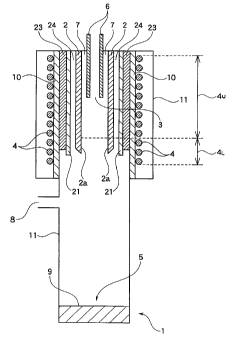
be described with reference to the drawings. Fig. 1 is a
sectional view of an embodiment of the silicon production
apparatus according to the invention. The members and items
common to those of the aforesaid conventional silicon
production apparatus will be indicated with
smaller-by-hundred numbers.
As illustrated, a silicon production apparatus 1 has a
closed vessel 11 that includes a reaction tube 2, a gas supply
opening 3 for supplying a chlorosilane and hydrogen, a high
frequency heating coil 4 provided around the outer periphery
CA 02517764 2005-08-31
SF-1089
12
of the reaction tube 2, and a carbon tube 21 provided adjacent
to the outer peripheral surface of the reaction tube 2,
extending from an upper part to near a lower end portion 2a
of the reaction tube.
The chlorosilanes for use in the reaction include
trichlorosilane (SiHCl3), silicon tetrachloride (SiClq),
dichlorosilane (SiH2C12) , monochlorosilane (SiH3C1) ,
chlorodisilanes such as hexachlorodisilane (Si2Cl6), and
chlorotrisilanes such as octachlorotrisilane (Si3Cle) . These
chlorosilanes may be used singly or in combination of two or
more kinds.
The reaction tube 2 is a cylindrical tube and is open
downward at an opening in the lower end portion 2a. The
reaction tube is suitably made of a carbon material such as
graphite, which can undergo high frequency heating and is
resistant to the melting point of silicon.
To enhance the durability of the reaction tube 2 and to
improve the silicon purity, the inner tube surface that is
brought into direct contact with deposited silicon is
preferably coated with silicon nitride, silicon carbide or
pyrolytic carbon which has a relatively high resistance to the
silicon melt.
Into the reaction tube 2, the chlorosilane and hydrogen
are supplied together or separately through the gas supply
CA 02517764 2005-08-31
SF-1089
13
opening 3 of a gas supply tube 6 provided above . The gas supply
tube 6 is preferably equipped with cooling means for cooling
the gas supply tube 6 to prevent thermal deterioration of the
tube and to prevent the chlorosilane from decomposing within
the tube. For example, the cooling of the gas supply tube 6
may be performed as follows. The gas supply tube 6 is fitted
with a channel in which a refrigerant liquid such as water or
heat transfer oil is circulated for cooling (fluid jacket
system). Alternatively, one or more nozzles are arranged
around the outer periphery of the gas supply tube 6 in a
substantially concentric configuration, and the reaction gas
is supplied through the gas supply tube 6 and simultaneously
the gas supply tube 6 is cooled by feeding (purging) a cooling
gas into the gap between the gas supply tube 6 and the nozzles
(air cooling jacket system).
The inner surface of the reaction tube 2 and the outer
surface of the gas supply tube 6 are laterally superposed on
one another in an upper region of the reaction tube 2. Since
this region is a low temperature region, it is difficult to
melt the solid silicon deposited in this region by heating to
a temperature equal to or in excess of its melting point.
Therefore, a seal gas such as hydrogen or argon gas is supplied
to a gap 7 between the reaction tube 2 and the gas supply tube
6 to fill the gap 7 with the seal gas atmosphere, thereby
CA 02517764 2005-08-31
SF-1089
14
preventing the chlorosilane/hydrogen mixed gas from filling
the gap 7 . Alternatively, a reagent such as hydrogen chloride
that produces a feedstock gas by reaction with silicon may be
supplied to the gap 7 singly or in combination with the seal
gas.
Other regions in the production apparatus 1 where the
silicon deposition should be avoided, such as a gap 24 between
the reaction tube 2 and the carbon tube 21, are similarly filled
with a seal gas or the like.
The reaction tube 2 is heated with an electromagnetic
wave (high frequency wave) from the peripherally-provided high
frequency heating coil 4, and the inner surface of the reaction
tube 2 is brought to a temperature equal to or in excess of
the melting point of silicon or to a temperature below the
melting point at which silicon deposition is feasible. The
heating region generally ranges from the lower end portion 2a
to a length in the tube direction that is 30 to 900 of the total
length of the reaction tube 2 in the closed vessel 11.
When the silicon deposition is performed while the inner
surface of the reaction tube 2 has a temperature equal to or
in excess of the melting point of silicon ( first method) , the
inner surface of the reaction tube 2 is brought to or above
the melting point of silicon (generally from 1410 to 1430°C)
and the silicon is deposited in a molten state.
CA 02517764 2005-08-31
SF-1089
When the silicon deposition is performed while the inner
surface of the reaction tube 2 has a temperature below the
melting point at which silicon deposition is feasible (second
method) , the temperature of the inner surface of the reaction
5 tube 2 will be 950°C or above, preferably 1200°C or above, and
more preferably 1300°C or above.
The high frequency heating coil 4 generates an
electromagnetic wave to heat the reaction tube 2 by the passage
of electric current through the coil 4 from a power source (not
10 shown). The frequency of the electromagnetic wave is
determined appropriately depending on the material or shape
of the heating obj ect such as the heating tube 2 . For example,
the frequency is set at approximately several tens of Hz to
several tens of GHz.
15 The silicon deposited on the inner surface of the
reaction tube 2 is caused to drip down from an opening at the
lower end portion 2a of the reaction tube 2, and is collected
in a silicon collection part 5 provided underneath.
The silicon collection part 5 has a cooling collection
part made of such a material as a metal, ceramic or glass. To
achieve toughness as industrial equipment and to collect high
purity silicon, it is preferable that the inner surface of the
metal cooling collection part is lined with silicon, Teflon
(trade name), quartz glass, tantalum, tungsten or molybdenum.
CA 02517764 2005-08-31
SF-1089
16
It is also appropriate to cover the upper bottom surface of
the cooling collection part with silicon particles. Further,
a withdrawal opening may be provided to permit continual or
intermittent withdrawal of the solidified silicon from the
cooling collection part. The silicon that has reached the
cooling collection part is cooled by contact with the aforesaid
material. Alternatively, the cooling may be conducted by
providing a cooling jacket in which a refrigerant liquid is
circulated, or a cooling gas supply tube for supplying a cooling
gas.
In the aforesaid first method, the silicon melt deposited
in a molten state is allowed to continually drip down from the
opening at the lower end portion 2a of the reaction tube 2 and
is collected in the silicon collection part 5 provided
underneath. In this case, the deposited silicon melt flows
downward on the inner surface of the reaction tube 2 and drips
down by gravity from the lower end portion 2a. The drops
solidify during or after the gravity fall.
In the second method, the solid silicon is temporarily
deposited on the inner surface of the reaction tube 2 and the
inner surface is heated to a temperature equal to or in excess
of the silicon melting point, so that part or whole of the
deposit is molten and is caused to drip down into the silicon
collection part 5 provided underneath, in which the silicon
CA 02517764 2005-08-31
SF-1089
17
is collected.
This method repeats the step of depositing silicon on
the inner surface of the reaction tube 2 and the step of heating
the inner surface to a temperature equal to or in excess of
the melting point of silicon to drop the deposit and collect
it in the silicon collection part 5. In the withdrawal of the
silicon 9 from the collection part 5 to outside the apparatus,
a plate-like member may be provided such that it is laterally
slidable so as to partition the inside of the apparatus into
an upper space including the reaction tube 2 and a lower space
including the collection part 5. According to this
configuration, the deposition reaction can be continually
performed while maintaining the reaction gas atmosphere in the
upper space of the apparatus, and the silicon 9 collected in
the collection part 5 can be withdrawn to outside the apparatus .
Meanwhile, the heating of the inner surface of the reaction
tube 2 to or above the melting point of silicon may be
accomplished by manipulating the power output of the high
frequency heating coil 4. Alternatively, the heating can be
accomplished by reducing the flow rate of the gas flowing in
the silicon production apparatus 1.
There is particularly no limitation on silicon
production conditions. Preferably, conditions such as the
chlorosilane/hydrogen feed ratio, feed rate and dwell time are
CA 02517764 2005-08-31
SF-1089
18
determined such that the chlorosilane-to-silicon conversion
will be at least 20 0, and preferably at least 30 0 . To achieve
an efficient production rate of silicon relative to the
reaction apparatus size, the molar fraction of the
chlorosilane to the gas supplied is preferably in the range
of 0 . 1 to 99 . 9 mol o, and more preferably 5 to 50 mol o . Although
the higher the reaction pressure, the more downsized the
apparatus, the pressure will range from about 0 to 1 MPaG
because of easy industrial implementation.
The gas dwell time may vary depending on the pressure
and temperature conditions with a specific-volume reaction
apparatus. Under the reaction conditions, the average dwell
time of the gas in the reaction tube 2 will be in the range
of 0.001 to 60 seconds, and preferably 0.01 to 10 seconds, in
which case a sufficiently efficient conversion of the
chlorosilane can be achieved.
When the inner surface of the reaction tube 2 is heated
by the high frequency heating coil 4 to or above the melting
paint of silicon to cause the silicon to drip down from the
lower end portion 2a of the reaction tube 2 and to collect it
in the silicon collection part 5, the lower end portion 2a has
particularly great heat release and thus cannot be heated
sufficiently, resulting in a lower temperature relative to the
upper inner surface of the tube. Consequently, the silicon
CA 02517764 2005-08-31
SF-1089
19
melt is cooled at the lower end portion 2a and is partially
solidified.
The solidification of the silicon melt at the lower end
portion 2a results in growth of a silicon mass hanging like
an icicle from the tip of the lower end portion 2a. Thus, the
silicon melt cannot be dropped and collected in the silicon
collection part 5 appropriately.
To solve this problem, the present invention provides
temperature lowering prevention means for preventing
temperature lowering in the lower end portion 2a when the
reaction tube 2 is heated to or above the melting point of
silicon. Specifically, the temperature lowering prevention
means is a device or a member capable of heating the lower end
portion 2a such that the lower end portion 2a has a temperature
equal to or in excess of the silicon melting point, preferably
1430 to 1500°C. The lower end portion 2a should be prevented
from being overheated with the temperature lowering prevention
means because otherwise undesirable silicon fine powder will
result.
The range of the lower end portion 2a to be heated with
the temperature lowering prevention means may vary depending
on its shape or the like. For example, as illustrated in Fig.
9 (a) , the lower end portion 2a to be heated with the temperature
lowering prevention means will range up to a horizontal surface
CA 02517764 2005-08-31
SF-1089
72 passing through intersections 74 between:
straight lines extending from an intersection 73 of a
horizontal surface (opening surface) 71 leveling with the
lowermost end of the reaction tube 2 and the central axis of
5 the reaction tube 2, the straight lines each having an angle
of 45 degrees relative to the opening surface 71; and
perpendicular lines extending along the inner
peripheral surface of the reaction tube 2 in the axial direction,
the perpendicular lines originatingfrom the shortest straight
10 line of the straight lines halving the opening surface 71 (for
example, when the opening surface 71 has an elliptical shape,
the shortest straight line is the minor axis) . The larger the
opening diameter of the reaction tube 2, the greater the heat
release from the lower end portion 2a, so that the lower end
15 portion 2a to be heated is extended.
The opening shape of the reaction tube 2 may be a circular
shape or other shape such as an elliptical shape. The lower
end portion 2a in the vicinity of the opening may have a uniform
thickness from above to the lowermost end. In another
20 embodiment, to control the droplet of the silicon melt such
that the silicon particles have small and uniform diameters,
the outer peripheral portion may be tapered such that the
diameter is gradually reduced toward the lowermost end.
Furthermore, the peripheral edge of the opening may have a wavy
CA 02517764 2005-08-31
SF-1089
21
form.
The opening surface of the reaction tube 2 may be tilted
relative to the horizontal level. In this case, as illustrated
in Fig. 9(b), the lower end portion 2a to be heated with the
temperature lowering prevention means will range up to a
surface 72 that is parallel to an opening surface 71 and has
identical distances from intersections 74a and 74b between:
straight lines extending from an intersection 73 of the
opening surface 71 of the reaction tube 2 and the central axis
of the reaction tube 2, the straight lines each having an angle
of 45 degrees relative to the opening surface 71; and
perpendicular lines extending along the inner
peripheral surface of the reaction tube 2 in the axial direction,
the perpendicular lines originatingfrom the shortest straight
line of the straight lines halving the opening surface 71.
The height of the lower end portion 2a to be heated can
be generally determined based on the Figs. 9(a) and (b) even
when the lower end portion 2a of the reaction tube 2 has a
complicated form.
It is necessary that the temperature lowering prevention
means heats a region that covers the lower end portion 2a
(portion from the lowermost end of the reaction tube 2 to a
distance r in the tube axial direction) , as shown in Fig. 10.
The heating region is desirably extended as required to a length
CA 02517764 2005-08-31
SF-1089
22
4 times the distance r (distance 4r) . When the reaction tube
2 is heated with the temperature lowering prevention means to
a length exceeding the distance 4r, silicon fine powder often
results.
In the apparatus of the present invention, a section of
the reaction tube 2 in which silicon is deposited (silicon
deposition section) has a length L (see Fig. 11) such that the
ratio (L/D) of the length L to an inner diameter D of the
reaction tube 2 at the lowermost end is at least 2, and
preferably at least 3.
In a preferred embodiment, the apparatus includes a
thermal insulating member 23 that is provided around the outer
periphery of the reaction tube 2 to prevent the heat release
from the reaction tube 2 during heating. The provision of the
thermal insulating member is not compulsory, and may be omitted
depending on the case . Even when the thermal insulating member
23 covers the reaction tube 2 to the lowermost end of the lower
end portion 2a, the temperature lowering at the lower end
portion 2a occurs due to the heat release from the inner surface
of the lower end portion 2a. The temperature lowering at the
lower end portion 2a will be more significant if the thermal
insulating member 23 does not cover the reaction tube 2 to the
lower end portion 2a.
In the embodiment shown in Fig. 1, the temperature
CA 02517764 2005-08-31
SF-1089
23
lowering at the lower end portion 2a is prevented by providing
a carbon tube 21 that is adj acent to the lower end portion 2a
while surrounding the outer periphery thereof. The carbon
tube 21 is mainly made of a carbon material, such as graphite,
that can be heated with high frequency waves from the high
frequency heating coil 4.
The lower end portion 2a of the reaction tube 2 is heated
directly by the high frequency heating coil 4 and
simultaneously with the infrared rays from the carbon tube 21
that is heated by the high frequency heating coil 4.
Because of the additional heating with the infrared rays
from the carbon tube 21, the lower end portion 2a can be heated
sufficiently to a temperature equal to or above the melting
point of silicon. Accordingly, the silicon melt will not be
cooled in this portion to cause a silicon mass, and the silicon
melt can flow on the inner surface of the reaction tube 2 and
smoothly drip down from the lower end portion 2a into the
silicon collection part 5.
In the present embodiment, the carbon tube 21 is provided
in between the reaction tube 2 and the peripherally-provided
thermal insulating member 23 made of carbon fibers or sintered
ceramic, such that the thermal insulating member 23 is wound
around the outer peripheral surface of the carbon tube 21 . The
gap 24 between the reaction tube 2 and the carbon tube 21 is
CA 02517764 2005-08-31
SF-1089
24
filled with a seal gas such as hydrogen to prevent the
deposition of silicon in this region. In this case, the
tubular member such as the carbon tube 21 that is interposed
between the reaction tube 2 and the thermal insulating member
23 may be formed such that a part thereof including a lower
end portion is made of a carbon material and the remaining upper
part is made of a material, such as a ceramic, that is not heated
with the high frequency wave from the high frequency heating
coil 4. That is, the infrared heating of the lower end portion
2a can be performed properly if the tubular member in the
vicinity of the lower end portion 2a of the reaction tube 2
is made of a carbon material, and the remaining part of the
tubular member may be made of a material other than the carbon
material.
In another embodiment, as illustrated in Fig. 2, the
thermal insulating member 23 may be wound around the outer
periphery of the reaction tube 2, and the carbon tube 21 may
be provided only in the vicinity of the lower end portion 2a
of the reaction tube 2. To permit the high frequency wave from
the high frequency heating coil 4 to effectively reach the lower
end portion 2a of the reaction tube 2, the thickness in the
diameter direction of the carbon tube 21 is desirably small
without deteriorating the strength and the like in view of the
penetration depth depending on the frequency.
CA 02517764 2005-08-31
SF-1089
Figs. 3 and 4 are views showing the vicinity of the
reaction tube lower end portion in other embodiments of the
silicon production apparatus of the present invention. In the
Fig. 3 embodiment, a ring-shaped heating unit 31 is arranged
5 in the vicinity of the lower end portion 2a of the reaction
tube 2. An electric current is supplied to the ring-shaped
heating unit 31 from a power source (not shown), and the
ring-shaped heating unit 31 is energized and radiates infrared
rays to the lower end portion 2a to heat the same.
10 In the Fig. 4 embodiment, a plurality of rod-shaped
members 41 made of quartz glass are arranged in the vicinity
of the lower end portion 2a of the reaction tube 2 . The infrared
light from an electric bulb 42 is introduced into the rod-shaped
member 41 from a rear end portion 41a'thereof and is guided
15 to a front end portion 41b. The infrared light having reached
the front end portion 41b is spot applied to the lower end
portion 2a to heat the same. The front end portion 41b of the
rod-shaped quartz glass member 41 is desirably formed like a
lens to focus the infrared light.
20 The aforesaid embodiments employ infrared rays to heat
the lower end portion 2a of the reaction tube 2 to prevent the
temperature lowering. Preferably, the infrared rays are
applied to the entire peripheral surface of the lower end
portion 2a.
CA 02517764 2005-08-31
SF-1089
26
Fig. S is a sectional view showing the vicinity of the
reaction tube lower end portion in another embodiment of the
silicon production apparatus. In the present embodiment, the
high frequency heating coil 4 is formed such that a coil (lower
end coil 4L) near the lower end portion 2a of the reaction tube
2 has smaller coil pitches Pl than coil pitches P2 of an upper
coil 4U. (Refer to Fig. 1 for the arrangement of the lower
end coil 4L and coil 4U.)
When the lower end coil 4L has an increased winding
density as described above, the high frequency heating coil
4 can heat the reaction tube 2 such that the lower end portion
2a is strongly heated selectively by the lower end coil 4L
having a high winding density, and the temperature lowering
at the lower end portion 2a is prevented.
The high frequency heating coil 4 is supplied with
electricity from a single power source. When electricity is
supplied to the high frequency heating coil 4 from one end to
the other in which the coil consists of the lower end coil 4L
and the upper coil 4U with different winding densities, the
lower end coil 4L having smaller coil pitches emits a high
frequency wave with a higher intensity than that from the upper
coil 4U. Accordingly, the lower end portion 2a of the reaction
tube 2 is strongly heated selectively. Since the heating of
the lower end portion 2a and upper portion of the reaction tube
CA 02517764 2005-08-31
SF-1089
27
2 can be performed with a single power source, the apparatus
structure can be relatively simplified.
In view of prevention of silicon mass formation at the
lower end portion 2a of the reaction tube 2, the coil pitches
P1 and P2 of the lower end coil 4L and upper coil 4U preferably
have a coil pitch ratio P2/P1 of at least 3, although dependent
on the apparatus structure.
Fig. 6 is a sectional view of a modification of the Fig.
5 embodiment . As illustrated, the carbon tube 21 is provided
in the vicinity of the lower end portion 2a of the reaction
tube 2. The carbon tube 21 is heated by the lower end coil
4L having a high winding density and emits infrared rays to
heat the lower end portion 2a of the reaction tube 2.
The lower end portion 2a of the reaction tube 2 is
strongly heated selectively by the lower end coil 4L having
a high winding density. In addition, the lower end portion
is heated with the infrared rays from the carbon tube 21 heated
with the high frequency wave from the lower end coil 4L.
Accordingly, the temperature lowering at the lower end portion
2a of the reaction tube 2 can be effectively prevented.
Fig. 7 is a sectional view showing the vicinity of the
reaction tube lower end portion in another embodiment of the
silicon production apparatus. In the present embodiment, the
high frequency heating coil 4 near the lower end portion 2a
CA 02517764 2005-08-31
SF-1089
28
of the reaction tube 2 includes two coils (lower end coils 4L)
that are double wound in the diameter expanding direction.
When the reaction tube 2 is heated by the high frequency
heating coil 4, the double-wound lower end coils 4L can heat
the lower end portion 2a of the reaction tube 2 by means of
the high frequency waves from both the inner and outer coils
of the lower end coils 4L. Accordingly, the heating can be
performed more strongly than by the upper coil 4U. Thus, the
lower end portion 2a of the reaction tube 2 is strongly heated
selectively, and the temperature lowering at the lower end
portion 2a is prevented.
The double-wound lower end coils 4L may be multilayer
coils wound at least threefold in the diameter expanding
direction.
When the lower end coil 4L is created by winding a single
coil into multilayer coils, the high frequency heating coil
4 may be supplied with electricity from a single power source.
Fig. 8 is a sectional view showing the vicinity of the
reaction tube lower end portion in another embodiment of the
silicon production apparatus. In the present embodiment, the
high frequency heating coil 4 consists of two individual coils
supplied with electricity from separate systems.
One coil 4U is arranged around the outer periphery of
the entire deposition section above the vicinity of the lower
CA 02517764 2005-08-31
SF-1089
29
end portion 2a of the reaction tube 2, and the other lower end
coil 4L is arranged in the vicinity of the lower end portion
2a of the reaction tube 2.
The coil 4U and the lower end coil 4L are controlled by
separate independent control systems to provide appropriate
high frequency power . The coil 4U heats the deposition section
above the lower end portion 2a of the reaction tube 2, and the
coil 4L heats the lower end portion 2a.
When the silicon is molten, the high frequency power is
controlled by the control systems such that the lower end coil
4L heats the lower end portion 2a of the reaction tube 2 with
a higher heating intensity than the upper coil 4L heats the
reaction tube 2. This control permits the lower end portion
2a of the reaction tube 2 to be selectively heated strongly
with the strong high frequency wave from the lower end coil
4L, so that the temperature lowering at the lower end portion
2a is prevented.
To control the high frequency power of the coil 4U and
that of the lower end coil 4L separately by independent systems,
separate power sources will be provided to supply electricity
to the coil 4U and the lower end coil ~L, and the coils will
be provided with high frequency power from the respective power
source.
Alternatively, the coil 4U and the lower end coil 4L can
CA 02517764 2005-08-31
SF-1089
be supplied with electricity from a single power source, and
independent power supply systems can be established with a tap
or a thyristor to provide the coils with high frequency power
from separate systems.
5 The supply of high frequency power to the lower end coil
4L is feedback controlled by measuring the temperature of the
lower end portion 2a of the reaction tube 2, or is manipulated
while visually observing the operation state.
The present invention will be described hereinbelow by
10 examples, but is not limited to the examples.
[Example 1]
A carbon-made cylindrical reaction tube 100 mm in outer
diameter, 70 mm in inner diameter and 1000 mm in length was
fitted in a polycrystalline silicon production apparatus.
15 Around the outer periphery of a lower end portion of the
reaction tube was arranged a carbon tube (21) as shown in Fig.
2, so that the reaction tube lower end portion would be heated
with infrared rays from the carbon tube heated by a high
frequency heating coil.
20 A mixed gas was fed into the reaction tube at rates of
20 kg/h for trichlorosilane and 40 Nm3/h for hydrogen. The
high frequency heating coil wound at regular pitches was
energized to heat the lower end portion and remaining upper
portion of the reaction tube to a temperature of 1450°C or above,
CA 02517764 2005-08-31
SF-1089
31
and polycrystalline silicon was deposited in a molten state.
After the reaction had been performed continually for 100 hours,
the lower end portion of the reaction tube was visually observed,
but no silicon mass had been solidified at the lower end portion
of the reaction tube.
[Example 2)
A carbon-made cylindrical reaction tube 100 mm in outer
diameter, 70 mm in inner diameter and 1000 mm in length was
fittedin a polycrystallinesilicon production apparatus. The
silicon production apparatus included a highfrequency heating
coil in which a lower end coil (4L) had smaller pitches and
a higher winding density, as illustrated in Fig. 5. The pitch
Pl of the lower end coil (4L) was 10 mm, and the pitch P2 of
the upper coil (4U) was 30 mm. This continually wound coil
was supplied with high frequency power from a single power
source.
A mixed gas was fed into the reaction tube at rates of
kg/h for trichlorosilane and 40 Nm3/h for hydrogen. The
high frequency heating coil was energized to heat the lower
20 end portion and remaining upper portion of the reaction tube
to a temperature of 1450°C or above, and polycrystalline
silicon was deposited in a molten state. After the reaction
had been performed continually for 100 hours, the lower end
portion of the reaction tube was visually observed, but no
CA 02517764 2005-08-31
SF-1089
32
silicon mass had been solidified at the lower end portion of
the reaction tube.
[Example 3]
A carbon-made cylindrical reaction tube 100 mm in outer
diameter, 70 mm in inner diameter and 1000 mm in length was
fitted in a polycrystalline silicon production apparatus. The
silicon production apparatus included a highfrequency heating
coil in which a lower end coil (4L) was double wound in the
diameter extending direction, as illustrated in Fig. 7.
A mixed gas was fed into the reaction tube at rates of
kg/h for trichlorosilane and 40 Nm3/h for hydrogen. The
high frequency heating coil was energized to heat the lower
end portion and remaining upper portion of the reaction tube
to a temperature of 1450°C or above, and polycrystalline
15 silicon was deposited in a molten state. After the reaction
had been performed continually for 100 hours, the lower end
portion of the reaction tube was visually observed, but no
silicon mass had been solidified at the lower end portion of
the reaction tube.
20 [Example 4]
A carbon-made cylindrical reaction tube 100 mm in outer
diameter, 70 mm in inner diameter and 1000 mm in length was
fittedin a polycrystalline silicon production apparatus. The
silicon production apparatus included a highfrequency heating
CA 02517764 2005-08-31
SF-1089
33
coil in which the high frequency power for a lower end coil
(4L) and an upper coil (4U) was separately controlled by
respective systems, as illustrated in Fig. 8. That is, the
lower end coil (4L) and the upper coil (4U) had separate power
sources, and the power supply to the separate coils was
controlled independently.
A mixed gas was fed into the reaction tube at rates of
20 kg/h for trichlorosilane and 40 Nm3/h for hydrogen. The
high frequency heating coil was energized to heat the lower
end portion and remaining upper portion of the reaction tube
to a temperature of 1450°C or above, and polycrystalline
silicon was deposited in a molten state. After the reaction
had been performed continually for 100 hours, the lower end
portion of the reaction tube was visually observed, but no
silicon mass had been solidified at the lower end portion of
the reaction tube.
[Comparative Example 1]
The reaction was carried out continually under the same
conditions as in Example l, except that the carbon tube (21)
was eliminated. The reaction resulted in solidification of
a silicon mass at the lower end portion of the reaction tube,
and the silicon had grown like an icicle. The silicon mass
prevented continuation of the reaction.
CA 02517764 2005-08-31
SF-1089
34
BRIEF DESCRIPTION OF THE DRAWINGS
Fig. 1 is a sectional view showing an embodiment of a
silicon production apparatus according to the present
invention;
Fig. 2 is a sectional view showing the vicinity of a
reaction tube lower end portion in a modification of the Fig.
1 embodiment;
Fig. 3 is a view showing the vicinity of a reaction tube
lower end portion in another embodiment of the silicon
production apparatus;
Fig. 4 is a view showing the vicinity of a reaction tube
lower end portion in another embodiment of the silicon
production apparatus;
Fig. 5 is a sectional view showing the vicinity of a
reaction tube lower end portion in another embodiment of the
silicon production apparatus;
Fig. 6 is a sectional view showing the vicinity of a
reaction tube lower end portion in a modification of the Fig.
5 embodiment;
Fig. 7 is a sectional view showing the vicinity of a
reaction tube lower end portion in another embodiment of the
silicon production apparatus;
Fig. 8 is a sectional view showing the vicinity of a
reaction tube lower end portion in another embodiment of the
CA 02517764 2005-08-31
SF-1089
silicon production apparatus;
Fig. 9 is a set of views for explaining the range of the
reaction tube lower end portion to be heated with temperature
lowering prevention means;
5 Fig. 10 is a view for explaining a region to be heated
with the temperature lowering prevention means;
Fig. 11 is a view for explaining a ratio L/D of a length
L of a silicon deposition section of the reaction tube to an
inner diameter D of the reaction tube at the lowermost end;
10 and
Fig. 12 is a sectional view showing a conventional
silicon production
apparatus;
wherein:
1 Silicon production apparatus
15 2 Reaction tube
2a Lower end portion
3 Gas supply opening
4 High frequency heating coil
4L Lower end coil
20 4U Upper coil
5 Collection part
6 Gas supply tube
7 Gap
8 Gas discharge opening
CA 02517764 2005-08-31
SF-1089
36
9 Collected silicon
Bulkhead wall
11 Closed vessel
21 Carbon tube
5 23 Thermal insulating member
24 Gap
31 Ring-shaped heating unit
41 Rod-shaped member
41a Rear end portion
10 41b Front end portion
42 Electric bulb
51 Lower end portion
52 Base
61 Lower end heating coil
71 Opening surface
72 Horizontal surface (parallel surface)
73 Intersection
74 Intersection
74a Intersection
74b Intersection
100 Silicon production apparatus
102 Reaction tube
102a Lower end portion
103 Gas supply opening
CA 02517764 2005-08-31
SF-1089
37
104 High frequency heating coil
105 Collection part
106 Gas supply tube
107 Gap
108 Gas discharge opening
109 Collected silicon
110 Bulkhead wall
111 Closed vessel
P1 Coil pitch
P2 Coil pitch
L Length of deposition section
D Inner diameter of reaction tube lower end