Note: Descriptions are shown in the official language in which they were submitted.
CA 02517771 2005-08-31
WO 2005/003790 PCT/US2004/020126
MAGNETIC RESONANCE IMAGING INTERFERENCE IMMUNEDEVICE
TECHNICAL FIELD
The present invention is directed to a device for protecting a patient,
physician, and/or
electronic components in an electrical device implanted or partially implanted
within the
patient. More particularly, the present invention is directed to a device for
protecting the
conductive parts of the electrical device from current and voltage surges
induced by magnetic
resonance imaging systems' oscillating magnetic fields.
i o BACKGROUND ART
Magnetic resonance imaging (''MR.I") has been developed as an imaging
technique
adapted to obtain both images of anatomical features of human patients as well
as some aspects
of the functional activities and characteristics of biological tissue. These
images have medical
diagnostic value in determining the slate of the health of the tissue
examined. Unlike the
situation with Fluoroscopic imaging, a patient undergoing magnetic resonance
imaging
procedure may remain in the active imaging system for a significant amount of
time, e.g. a
half hour or more, without suffering any adverse effects.
In an MRI process, a patient is typically aligned to place the portion of the
patient's
anatomy to be examined in the imaging volume ofthe MRI apparatus. Such an MRI
apparatus
typically comprises a primary electromagnet for supplying a constant magnetic
field (Bo)
which, by convention, is along the z-axis a~ld is substantially homogeneous
over the imaging
volume and secondary electromagnets that can provide linear magnetic field
gradients along
each of three principal Cartesian axes in space (generally x, y, and z, or xl,
x~ and x"
respectively). The MRI apparatus also comprises one or more RF (radio
frequency) coils that
provide excitation and detection of the MRI induced signals in the patient's
body.
The gradient fields are switched ON and OFF at different rates depending on
the MRI
scan sequence used. 1n some cases, this rnay result in a changing magnetic
field on the order of
dBldt = 50 T/s. The frequency that a gradient field may be turned ON can be
between 200Hz
to about 3001;Hz.
For a single loop with a fixed area, Lenz's law can be stated as:
~MF = - A ~ dBldt
where A is the area vector, B is the magnetic field vector, and "~" is the
vector scalar product.
This equation indicates that an electro-motive=force (EMF) is developed in any
loop that
encircles a changing magnetic field.
In an MRI system, there is applied to the biological sample (patient) a
switched
gradient field in all 3 coordinate directions (x-, y-, z- directions). If the
patient has an
-1
CA 02517771 2005-08-31
WO 2005/003790 PCT/US2004/020126
implanted heart pacemaker (or other implanted devices having conductive
components) the
switched gradient magnetic fields (an alternating magnetic field) may cause:
1. Erroneous signals to be induced/generated in a sensing lead or device
or circmt;
s 2. Damage to electronics; andlor
3. Harmful stimulation of tissue, e.g. hears: muscle, nerves, etc.
As noted above, the use of the MRI process with patients who have implanted
medical
assist devices; such as cardiac assist devices or implanted insulin pumps;
ofl:en presents
problems. As is lcnovvn to those skilled in the art, implantable devices (such
as implantable
l0 pulse generators (IPGs) and cardioverterl delibrillatorlpacemalcers (CDPs))
are sensitive to a
variety of forms of electromagnetic interference (EMI) because these
enumerated devices
include sensing and logic systems that respond to low-level electrical signals
emanating from
the monitored tissue region of the patient. Since the sensing systems and
conductive elements
of tlhese implantable devices are responsive to changes in local
electromagnetic fields, the
is implanted devices are vulnerable to e~temal sources of severe
electromagnetic noise, and in
particular, to electromagnetic fields emitted during the magnetic resonance
imaging (MRI)
procedure. Thus, patients with implantable devices are generally advised not
to undergo
magnetic resonance imaging (MRI) procedures.
To more appreciate the problem, the use of implantable cardiac assist devices
during a
2o MRI process will be briefly discussed.
The human heart may suffer from two classes of rhythmic disorders or
arrhythmias:
bradycardia and tachyarrhytlunia. Bradycardia occurs when the heart beats too
slowly, and
may be treated by a common implantable pacemaker delivering low voltage (about
3 V) pacing
pulses.
2s The common implantable pacemaker is usually contained within a hermetically
sealed
enclosure, in order to protect the operational components of the device from
the harsh
environment of the body, as well as to protect the body from the device.
The common implantable pacemaker operates in conjunction with one or more
electrically conductive leads, adapted to conduct electrical stimulating
pulses to sites within the
3o patient's heart, and to communicate sensed signals from those sites back to
the implanted
device.
Furthermore, the common irnplantable pacemaker typically has a metal case and
a
connector block mounted to the metal case that includes receptacles for leads
which may be
used for electrical stimulation ox which may be used for sensing of
physiological signals. The
35 battery and the circuitry associated with the common implantable pacemaker
are hermetically
-2-
CA 02517771 2005-08-31
WO 2005/003790 PCT/US2004/020126
sealed within the case. Electrical interfaces are employed to connect the
leads outside the
metal case with the medical device circuitry and the battery inside the metal
case.
Electrical interfaces serve the purpose of providing an electrical circuit
path extending
from the interior of a hermetically sealed metal case to an external point
outside the case while
maintaining the hermetic seal of the case. A conductive path is provided
through the interface
by a conductive pin that is electrically insulated from the case itself.
Such interfaces typically include a ferrule that permits atlaclunent of the
interface to the
case, the conductive pin, and a hermetic glass or ceramic seal that supports
the pin within the
ferrule and isolates the pin from the metal case.
to A common implantable pacemaker can, tinder some circumstances, be
susceptible to
electrical interference such that the desired functionality of the pacemaker
is impaired. For
example, common implantable pacemalter requires protection against electrical
interference
from electromagnetic interference (EMI), defibrillation pulses, electrostatic
discharge, or other
generally large voltages or currents generated by other devices external to
the medical device.
As noted above, more recently, it has become crucial that cardiac assist
systems be protected
from magnetic-resonance imaging sources.
Such electrical interference can damage the circuitry of the cardiac assist
systems or
cause interference in the proper operation or functionality of the cardiac
assist systems. For
example, damage may occur due to high voltages ox excessive currents
introduced into the
2o cardiac assist system.
Moreover, problems are realized when the placement of the implant is next to
pal-ticular
organs. For example, when a pacemaker is placed in the upper chest and the
lead tip is placed
into the heart, a loop (an electrical loop) is created. A changing magnetic
field (the switched
gradient field) over the area of the loop (through the area of the loop) will
cause an induced
voltage (md current) across the heart. This induced voltage (current) cm
stimulate the heart
inappropriately and can cause heart damage or death.
Therefore, it is desirable to provide a medical device or system that reduces
or
eliminates the undesirable effects of changing magnetic fields from an MRI
system on the
medical devices and/or patients undergoing medical procedures or that have
temporary or
3o permanent implanted materials andlor devices with conducting components.
DISCLOSURE OF INVENTION
A first aspect of the present invention is a voltage compensation unit for
reducing the
effects of induced voltages upon a device to a safe level. The voltage
compensation unit
includes a sensing circuit to sense voltages induced in conductive components
of the device,
3s the voltages being induced by changing magnetic fields and a compensation
circuit, operatively
-3-
CA 02517771 2005-08-31
WO 2005/003790 PCT/US2004/020126
connected to the sensing circuit and responsive thereto, to provide opposing
voltages to the
device to reduce the effects of induced voltages caused by changing magnetic
Fields.
A second aspect of the present invention is a voltage compensation unit for
reducing the
effects of induced voltages upon a tissue invasive medical tool to a safe
level. The voltage
compensation unit includes a sensing circuit to sense voltages induced in
conductive
components of the medical tool, the voltages being induced by changing
magnetic Fields; a
compensation circuit, operatively connected to the sensing circuit and
responsive thereto, to
provide opposing voltages to the medical tool to reduce the effects of induced
voltages caused
by changing magnetic Fields; and a connection device to provide an electrical
connection
1o between the sensing circuit and the compensation circuit and the medical
tool.
A third aspect of the present invention is a voltage compensation unit for
reducing the
effects of induced voltages upon a device to a safe level. The voltage
compensation unit
includes a communication circuit, communicatively linked to a MRI system, to
receive
information associated with a start and end of an application of changing
magnetic Fields
produced by the MRI system and a compensation circuit, operatively connected
to the
communication circuit and responsive thereto, to synchronize application of
opposing voltages
to the device with the sensed changing magnetic Fields, the opposing voltages
reducing the
effects of induced voltages caused by the changing magnetic fields.
A fourth aspect of the present invention is a voltage compensation uz>it for
reducing the
2o effects of induced voltages upon a device to a safe level. The voltage
compensation unit
includes a communication circuit, communicatively linked to a MRI system, to
receive
information associated with a start and end of an application of changing
magnetic Fields
produced by the MRI system and a compensation circuit, operatively connected
to the
coznznunication circuit and responsive thereto, to apply opposing voltages to
the device, the
opposing voltages reducing the effects of induced voltages caused by the
changing magnetic
gelds.
A Fifth aspect of the present invention is a voltage compensation unit for
reducing the
effects of induced voltages upon a device having a single wire line, the
single wire line having
a balanced characteristic impedance. The voltage compensation unit includes a
tunable
compensation circuit, operatively connected to the wire line, to apply
supplemental impedance
to the wire line, the supplemental impedance causing the characteristic
impedance of the wire
line to become unbalanced, thereby reducing the effects of induced voltages
caused by
changing magnetic fields.
Another aspect of the present invention is an electrical lead component for a
medical
device which reduces the effects of MRI induced signals to a safe level. The
electrical lead
component includes a medical device electrical lead capable of providing an
electrical path to a
-4-
CA 02517771 2005-08-31
WO 2005/003790 PCT/US2004/020126
desired tissue region and a coil that generates a changing MRI electromagnetic
field induced
current opposite to that which would be induced by the changing MRI
electromagnetic field in
the medical device electrical lead so as to reduce voltages induced by the
changing MRI
electromagnetic field to a safe level.
Another aspect of the present invention is an electrical lead component fox a
medical
device which reduces the effects of MRI induced signals to a safe level. The
electrical lead
component includes a medical device electrical lead capable of providing an
eleci~rical path to a
desired tissue region and a plurality of coils, each coil generating a
changing MRI
electromagnetic field induced current such a combination of changing MRI
electromagnetic
l0 field induced currents provide a combined current that is opposite to that
which would be
induced by the changing MRI electromagnetic field in the medical device
electrical lead so as
to reduce voltages induced by the changing MRI electromagnetic field to a sate
level.
Another aspect of the present invention is an electrical lead component for a
medical
device which reduces the effects of MRI induced signals to a safe level. The
electrical lead
component includes a medical device electrical lead capable of providing an
electrical path to a
desired tissue region and three orthogonally planar coils, each coil
generating a changing MRI
electromagnetic field induced current such a combination of the changing MRI
electromagnetic
field induced currents provide a combined current that is opposite to that
which would be
induced by the changing MRI electromagnetic field in the medical device
electrical lead so as
2o to reduce voltages induced by the changing MRI electromagnetic field to a
safe level.
Another aspect of the present invention is an electrical lead component for a
medical
device which reduces the effects of MRI induced signals to a safe level. The
electrical lead
component includes a medical device electrical lead capable of providing an
electrical path to a
desired tissue region; a plurality of coils, each coil generating a changing
MRI electromagnetic
field induced current; a sensor to measure a strength of voltages induced by
the changing MRI
electromagnetic field; and a switching device, operatively connected to the
sensor and plurality
of coils, to operatively connect a number of the plurality of coils in
response to the measured
strength of voltages induced by the changing MRI electromagnetic field such
that a
combination of the changing MRI electromagnetic field induced currents
produced by the
3o number of operatively connected switches provide a combined current that is
opposite to that
which would be induced by the changing MRI electromagnetic field in the
medical device
electrical lead so as to reduce voltages induced by the changing MRI
electromagnetic Field to a
safe level.
Another aspect of the present invention is an electrical lead component for a
medical
device which reduces the effects of MRI induced signals to a safe level. The
electrical lead
component includes a medical device electrical lead capable of providing an
electrical path to a
-5
CA 02517771 2005-08-31
WO 2005/003790 PCT/US2004/020126
desired tissue region; three orthogonally planar coils, each coil generating a
changing MRI
electromagnetic field induced current; a sensor to measure a strength of
voltages induced by
the changing MRI electromagnetic field; and a switching device, operatively
connected to the
sensor and the coils, to operatively connect a number of the coils in response
to the measured
strength of voltages induced by the changing MRI electromagnetic field such
that a
combination of the changing MRI electromagnetic field induced currents
produced by the
number of operatively connected switches provide a combined current that is
opposite to that
which would be induced by the changing MRI electromagnetic field in the
medical device
electrical lead so as to reduce voltages induced by the changing MRI
electromagnetic field to a
1o safe level.
Another aspect of the present invention is an electrical lead component for a
medical
device which reduces the effects of MRI induced signals to a safe level. The
electrical lead
component includes a medical device electrical lead capable of providing an
electrical path to a
desired tissue region; a plurality of coils, each coil generating a changing
MRI electromagnetic
field induced current; a transceiver to receive a signal indicating a number
of coils to be
connected; and a switching device,' operatively connected to the transceiver
and plurality of
coils, to operatively connect a number of the plurality of coils in response
to the received signal
indicating the number of coils to be connected such that a combination of the
changing MRI
electromagnetic field induced currents produced by the number of operai~ively
connected
2o switches provide a combined current that is opposite to that which would be
induced by the
changing MRr electromagnetic f eld in the medical device electrical lead so as
to reduce
voltages induced by the changing MRI electromagnetic field to a safe level.
Another aspect of the present invention is an electrical lead component for a
medical
device which reduces the effects of MRI induced signals to a safe level. The
electrical lead
component includes a medical device electrical lead capable of providing an
electrical path to a
desired tissue region; three orthogonally planar coils, each coil generating a
changing MRT
electromagnetic field induced current; a transceiver to receive a signal
indicating a number of
coils to be connected; and a switching device, operatively connected to the
transceiver and the
coils, to operatively connect a number of the coils in response to the
received signal indicating
30. the number of coils to be connected such that a combination of the
changing MRl
electromagnetic field induced currents produced by the number of operatively
connected
switches provide a combined current that is opposite to that which would be
induced by the
changing MRI electromagnetic f eld in the medical device electrical lead so as
to reduce
voltages induced by the changing MRI electromagnetic field to a safe level.
Another aspect of the present invention is a medical device which reduces the
effects of
MRI induced signals to a safe level. The medical device includes a medical
device capable of
-G
CA 02517771 2005-08-31
WO 2005/003790 PCT/US2004/020126
providing medical treatment to a desired tissue region and a coil that
generates a changing MRI
electromagnetic 1=field induced current opposite to that which would be
induced by the changing
MRI electromagnetic 'field in the medical device so as to reduce voltages
induced by the
changing MRI electromagnetic field to a safe level.
Another aspect of the present invention is a medical device which reduces the
effects of
MRI induced signals to a safe level. The medical device includes a medical
device capable of
providing medical treatment to a desired tissue region and a plurality of
coils, each coil
generating a changing MRI electromagnetic field induced current such a
combination of the
changing MRI electromagnetic field induced currents provide a combined current
that is
opposite to that which would be induced by the changing MRI electromagnetic
field in the
medical device so as to reduce voltages induced by the changing MRI
electromagnetic field to
a safe level.
Another aspect of the present invention is a medical device which reduces the
effects of
MRI induced signals to a safe level. The medical device includes a medical
device capable of
providing medical treatment to a desired tissue region and three orthogonally
planar coils, each
coil generating a changing MRI electromagnetic field induced current such a
combination of
the changing MRl electromagnetic field induced currents provide a combined
current that is
opposite to that which would be uiduced by the changing MRI electromagnetic
field in the
medical device so as to reduce voltages induced by the changing MRI
electromagnetic field to
a safe level.
Another aspect of the present invention is a medical device which reduces the
effects of
MRI induced signals to a safe level. The medical device includes a medical
device capable of
providing medical treatment to a desired tissue region; a plurality of coils,
each coil generating
a changing MRI electromagnetic field induced current; a sensor to measure a
strength or
voltages induced by the changing MRI electromagnetic field; and a switching
device,
operatively connected to the sensor and plurality of coils, to operatively
connect a number of
the plurality of coils in response to the measured strength of voltages
induced by the changing
MRI electromagnetic field such that a combination of the changing MRI
electromagnetic field
induced currents produced by the number of operatively connected switches
provide a
combined current that is opposite to that which would be induced by the
changing MRI
electromagnetic field in the medical device so as to reduce voltages induced
by the clmnging
MRI electromagnetic field to a safe level.
Another aspect of the present invention is a medical device which reduces the
effects of
MRI induced signals to a safe level. The medical device includes a medical
device capable of
3s providing medical treatment to a desired tissue region; three orthogonally
planar coil, each coil
generating a clmnging MRI electromagnetic field ilzduced current; a sensor to
measure a
_°7_
CA 02517771 2005-08-31
WO 2005/003790 PCT/US2004/020126
strength of voltages induced by the changing MRI electromagnetic field; and a
switching
device, operatively connected to the sensor and plurality or coils, to
operatively connect a
number of the plurality of coils in response to the measured strength of
voltages induced by
changing MRI electromagnetic field such that a combination of the changing MRI
electromagnetic field induced currents produced by the number of operatively
connected
switches provide a combined current that is opposite to that which would be
induced by the
changing MRI electromagnetic field in the medical device so as to reduce
voltages induced by
the changing MRI electromagnetic field to a safe level.
Another aspect of the present invention is a medical device which reduces the
effects of
1o MRl induced signals to a safe level. The medical device includes a medical
device capable of
providing medical treatment to a desired tissue region; a plurality of coils,
each coil generating
a changing MRI electromagnetic field induced current; a transceiver to receive
a signal
indicating a number of coils to be connected; and a switching device,
operatively connected to
the transceiver and the coils, to operatively connect a number of the coils in
response to the
received signal indicating the number of coils to be connected such that a
combination of the
changing MRI electromagnetic field induced currents produced by the number of
operatively
connected switches provide a combined current that is opposite to that whiclx
would be induced
by the changing MRI electromagnetic field in the medical device electrical
lead so as to reduce
voltages induced by changing MRI electromagnetic field to a safe level.
2o Another aspect of the present invention is a medical device which reduces
the effects of
MhRI induced signals to a safe level. The medical device includes a medical
device capable of
providing medical treatment to a desired tissue region; three orihogonally
planar coil, each coil
generating a changing MRI electromagnetic field induced current; a tT~nsceiver
to receive a
signal indicating a number of coils to be connected; and a switching device,
operatively
2s connected to the transceiver and the coils, to operatively connect a number
of the coils in
response to the received signal indicating the number of coils to be connected
such that a
combination of the changing MRI electromagnetic field induced currents
produced by tlxe
number of operatively connected s'vitches provide a combined current that is
opposite to that
which would be induced by the changing MRI electromagnetic field in the
medical device
3o electrical lead so as to reduce voltages induced by the changing MRI
electromagnetic field to a
safe level.
Another aspect of the present invention is a lead for medical applications
that reduces
the effects of MRI induced signals to a safe level. The lead includes two
coiled conductive
strands forming a spring-like configuration such that current flows over a
surface thereof,
3s through contact points between adjacent loops of the coiled conductive
strands and an
insulating coating formed over a pori:ion of the tzvo coiled conductive
strands such that an
_g_
CA 02517771 2005-08-31
WO 2005/003790 PCT/US2004/020126
inline inductive element is conned, the current flowing along a curvature of
the two coiled
conductive strands in the insulating coated portion of the two coiled
conductive strands.
Another aspect of the present invention is a lead for medical applications
that reduces
the effects of MRI induced signals to a safe level. The lead includes two
coiled conductive
strands forming a spring-like configuration such that current flows over a
surface thereof,
through contact points between adjacent loops of the coiled conductive stands
and an
adjustable resistive material formed over a portion of the two coiled
conductive strands such
that an inline inductive element is formed, the current flowing along a
curvature of the two
coiled conductive strands in the adjustable resistive material portion of the
two coiled
1 o conductive strands.
Another aspect of the present invention is a lead for medical applications
that reduces
the effects of MRI induced signals to a safe level. The lead includes a coiled
conductive strand
forming a spring-like configuration such that current flows over a surface
thereof, through
contact points between adjacent loops of the coiled conductive strand and ail
insulating coating
formed over a portion of the coiled conductive strand such that an inline
inductive element is
formed, the current flowing along a curvature of the coiled conductive strand
in the insulating
coated pori.ion of the coiled conductive stand.
Another aspect of the present invention is a lead for medical applications
that reduces
the effects of MRI induced signals to a safe level. The lead includes a coiled
conductive strand
2o forming a spring-like configuration such that current flows over a surface
thereof through
contact points between adjacent loops of the coiled conductive strand and an
adjustable
resistive material Formed over a portion of the coiled conductive strand such
that an mine
inductive element is formed, the current rowing along a curvature of the
coiled conductive
strand in the adjustable resistive material portion of the coiled conductive
strand.
Another aspect of the present invention is a lead for medical applications
that reduces
the effects of MRI induced signals to a safe level. The lead includes two
coiled conductive
strands forming a spring-like configuration such that current flows over a
surface thereof,
through contact points between adjacent loops of the coiled conductive
strlnds; a first
insulating coating formed over a first portion of the two coiled conductive
strands such that a
3o first inline inductive element having a first induci~nce is formed, the
current flowing along a
curvature of the two coiled conductive strands in the first insulating coated
portion of two
coiled conductive strands; and a second insulating coating formed over a
second portion of the
two coiled conductive strands such that a second inline inductive element
having a second
inductance is formed, the current Llowing along a curvature of the two coiled
conductive
stands in the second insulating coated portion of two coiled conductive
strands. The first
inductmce is different from the second inductance.
_9_
CA 02517771 2005-08-31
WO 2005/003790 PCT/US2004/020126
Another aspect of the present invention is a lead for medical applications
that reduces
the effects of MRI induced signals to a safe level. The lead includes two
coiled conductive
strands forming a spring-like configuration such that current flows over a
surface thereat;
through contact points betZVeen adjacent loops of the coiled conductive
strands; a rust
adjustable resistive material formed over a first portion of the two coiled
conductive strands
such that a first inline inductive element having a first inductance is
formed, the current
flowing along a curvature of the two coiled conductive strands in the first
adjustable resistive
material portion of the tzvo coiled conductive strands; and a second
adjustable resistive material
formed over a second portion of the two coiled conductive strands such that a
second inline
~o inductive element having a second inductance is formed, the current L7owing
along a curvature
of the two coiled conductive strands in the second adjustable resistive
material portion of the
two coiled conductive strands. The first inductance is different from the
second inductance.
Another aspect of the present invention is a lead for medical applications
that reduces
the effects of MRI induced signals to a safe level. The lead includes a coiled
conductive strand
forming a spring-like configuration such that current flows over a surface
thereof, through
contact points between adjacent loops of the coiled conductive strand; a first
insulating coating
formed over a first portion of the coiled conductive strand such that a first
inline inductive
element having a first inductance is fanned, the current flowing along a
curvature of the coiled
conductive strand in the first insulating coated portion of the coiled
conductive strand; and a
2o second insulating coating formed over a second portion of the coiled
conductive straild such
That a second inline inductive element having a second inductance is formed,
the current
flowing along a curvature of the coiled conductive strand in the second
insulating coated
portion of the coiled conductive strand. The first inductance is different
from the second
inductance.
Another aspect of the present invention is a lead for medical applications
that reduces
the effects of MRI induced signals to a safe level. The lead includes a coiled
conductive strand
forming a spring-like configuration such that current flows over a surface
thereof, through
contact pouits between adjacent loops of the coiled conductive strand; a Frst
adjustable
resistive material formed over a first portion of the coiled conductive strand
such that a first
3o inline inductive element having a f-~rst inductance is fomned, the current
slowing along a
curvature of the coiled conductive strand in the first adjustable resistive
material portion of the
coiled conductive strand; and a second adjustable resistive material formed
over a second
portion of the coiled conductive stand such that a second inline inductive
element having a
second inductance is formed, the current flowing along a curvature of the
coiled conductive
s5 strand in the second adjustable resistive material portion of the coiled
conductive strand. The
first inductance is different from the second induci~nce.
-10-
CA 02517771 2005-08-31
WO 2005/003790 PCT/US2004/020126
BRIEF DESCRIPTION OF THE DRAWINGS
The present invention may take form in various components and arrangements of
components, and in various steps and arrangements of steps. The drawings are
only fox
purposes of illustrating a preferred embodiment and are not to be construed as
limiting the
present invention, wherein:
Figure 1 is a schematic of an implanted pacemaker arrangement in a body;
Figure 2 is a schematic of a pacemaker lead comprising three conductive
strands;
Figure 3 is a schematic of a sensing system used with a pacemaker;
Figure 4 illustrates an embodiment of a pacemaker canister according to the
concepts of
1o the present invention;
Figure 5 illustrates another embodiment of a pacemaker canister according to
the
concepts of the present invention;
Figure 6 illustrates a further embodiment of a pacemaker canister according to
the
concepts of the present invention;
Figure 7 is an illustration of inductive currents in conductor loops;
Figure 8 is an illustration of canceling inductive currents in conductor loops
according
to the concepts of the present invention;
Figure 9 is a schematic of an embodiment of a pacemaker lead utilizing
inductive loops
according to the concepts of the present invention;
2o Figure 10 is a schematic of an embodiment of inductive loops in a pacemaker
canister
according to the concepts of the present invention;
Figure 11 is a schematic of an embodiment of inductive loops around a
pacemaker
canister according to the concepts of the present invention;
Figure 12 illustrates of an embodiment of a medical device with an external
voltage
cancellation unit according to the concepts of the present invention;
Figure 13 illustrates of another embodiment of a medical device with an
external
voltage cancellation unit according to the concepts of the present invention;
Figure 14 illustrates a portion of coiled leads used in a medial device
according to the
concepts of the present invention;
3o Figure 15 illustrates another embodiment of a portion of coiled leads used
in a medial
device according to the concepts of the present invention;
Figure 16 illustrates a further embodiment of a portion of coiled leads used
in a medial
device according to the concepts of the present invention;
Figure 17 illustrates another embodiment of a portion of coiled leads used in
a medial
device according to the concepts of the present invention;
-11-
CA 02517771 2005-08-31
WO 2005/003790 PCT/US2004/020126
Figure 18 illustrates a circuit diagram representing a guide wire with an
unbalancing
impedance circuit according to the concepts of the present invention;
Figure 19 illustrates another embodiment of a circuit diagram representing a
guide wire
with an unbalancing impedance circuit according to the concepts of the present
invention;
Figure 20 illustrates a balun used in conjunction with a guide wire according
to the
concepts of the present invention; and
Figure 21 is a circuit diagram representing a capacitance unbalanced balun
unit
according to the concepts ofthe present invention.
BEST MODE FOR CARRYING OUT THE INVENTION
1o The present invention will be described in connection with preferred
embodiments;
however, it will be understood that there is no intent to limit the present
invention to the
embodiments described herein. On the contrary, the intent is to cover all
alternatives,
modifications, and equivalents as may be included within the spirit and scope
of the present
invention as defined by the appended claims.
1s For a general understanding of the present invention, reference is made to
the drawings.
In the drawings, like reference have been used throughout to designate
identical or equivalent
elements. It is also noted that the various drawings illustrating the present
invention are not
drawn to scale and that certain regions have been purposely drawn
disproportionately so that
the features and concepts of the present invention could be properly
illustrated.
2o Figure 1 is a schematic showing a typical pacemaker arrangement 100. The
pacemaker
comprises a pulse generator canister 102 housing a power supply (not shown)
and electronic
components (not shown) for sensing and producing electrical pacing pulses. The
pulse
generator canister 102 has connected to it insulated conductive leads 104 that
pass through the
body (not shown) and into the heart 10G. Conventional bipolar pacemaker leads
have two
25 conductive strands, one for pacing and sensing, and the other for gromd.
The path of the leads
104 is generally not straight. The leads 104 have one or more electrodes 112
in contact with
the heart lOG. The direct line 108 from the heart 10G, where the electrodes
112 are placed, to
the generator canister 102 represents a conductive path comprising body tissue
(not shown) and
fluids (not shown). The completed loop from the pacemaker canister 102,
through the leads
30 104, and back to the pacemaker canister 102 along the path 108 is subject
to Lenz's law. That
is, a changing magnetic >Yield 110 through the area enclosed by the completed
loop (from the
pacemaker canister 102, through the leads 104, and back to the pacemaker
canister 102 along
the path 108) can induce unwanted voltages in the leads 104 and across the
heart 10G.
In one embodiment of the present invention, and referring to Figure 1, the
pacemaker
3s canister 102 is made out of a non-conductive material. In another
embodiment, the canister
102 is coated or covered with various non-conductive insulating materials.
Tlus increases the
_12_
CA 02517771 2005-08-31
WO 2005/003790 PCT/US2004/020126
overall resistance of the conductive path loop and thus reduces the voltage
across the tissue
bet<veen electrodes 112 and the canister 102.
Using a three-stand lead design allows for the separation of the pacing
signals from the
sensing signals and allows for different filtering techniques to be utilized
on each separate
conductive strand: one strand for the pacing signal For stimulating the heart,
one conductive
strand For the sensing of the heart's electrical state, pre-pulse, ecg, etc.,
and one strand For the
ground path. Current bi-polar designs use only two conductive strands. This
means that the
pacing and the sensing signals are carried on the same strand.
For example, in conventional bipolar pacemaker leads, the pacing signal goes
''down"
(from generator canister to heart) the pacing lead (conductive strand) while
the sensing signal
travels "up" (from heart to generator canister) the pacing lead. This is the
"standard" bipolar
pacing setup. IF a filter is added to the pacing/sensing strand to block the
switch gradient
induced signal caused by a MRI system, the pacing pulse/signal must travel
through the filter,
thereby distorting the pacing pulse.
According to the concepts of the present invention, by adding a third
conductive strand,
a diode, for example, can be put on the pacing strand and one or more filters
can be put on the
sensing strand. The Iilters on the sensing lead may be at the distal end of
the pacemaker lead
or in the generator canister. Thus, by using separate strands, the present
invention is able to
utilize different kinds of filters (RF filters, highllow pass filters, notch
filters, etc.) or other
2o electronics in conjunction with each strand depending on the different
signal characteristics
and/or signal direction along the conductive strand.
Figure 2 shows a schematic of a pacemaker arrangement 120 including a
generator
canister 122 containing a pacing pulse generator (not shown), sensing
electronics (not shown)
and other electronic components (not shown). Attached to the generator
canister 122 is a lead
assembly 140 having three conductive strands 124, 12G, and 12~ through lumen
138. Each of
the conductive strands 124, 12G, and 128 pass through the distal tip 142 of
the lead assembly
140 to exposed electrodes 132, 134, and 13G, respectively. The exposed
electrodes 132, 134,
and 13G are placed in contact with or nest to the heart.
Conductive strand 124 and electrode 132 are used to deliver pulses to the
heart From a
pacing generator within the canister 122. Conductive stand 12G and electrode
134 are used as
a ground. Conductive stand 128 and electrode 13G are utilized for sensing the
electrical
signals generated by the heart. In this way, the sensing functionality of
pacemakers can be
separated from the delivery of pacing pulses.
To block any induced voltage signals from the MRI system's changing magnetic
fields
(the RF or the gradient fields) from propagating along the conductive pulse
delivery strand
-13-
CA 02517771 2005-08-31
WO 2005/003790 PCT/US2004/020126
124, a diode 130 is inserted into the conductive strand 124 near the distal
tip of the lead
assembly 142. It is noted that the diode 130 can also be is placed ic1 the
generator canister 122.
With respect to Figure 2, other electronic components (i.e. RF Chocks, notch
filters,
etc.) rnay be placed into the other conductive strands 12G and 128 shown as by
components
14G and 144, respectively. It is noted that these optional electronic
components 14G and 144
can be placed in the generator canister 122.
Optional electronic components 14G and 144 are used to block or significantly
reduce
any unwanted induced signals caused by the MRI system from passing along
conductive
strands 12G and 128 respectively while allowing the desired sensing signals
from the heart to
to pass along conductive strand 12G to electronics in the generator canister
122.
Figure 3 is a schematic of an embodiment of the present invention. As
illustrated in
Figure 3, a patient 1G2 is located within an MRI system 1G8, wherein the
patient 1G2 has an
implanted heart pacemaker pulse generator canister 1G4. A surface
sensor/transceiver 1GG is
placed on the exterior of the patient's body 1G2 over or near the location of
the implanted
is pacemaker generator 1G4. The sensor/transceiver 1GG is in communication
with the MRI
system 1G8 via communication line 170, which may be an MRI safe cable such as
a fiber
optical cable. Additionally, the sensor/transceiver 1GG is in communication
with tile implanted
pacemaker pulse generator canister 1G4. The means of communication between the
sensor/transceiver 1GG a~~d the implanted pacemaker generator 1G4 may be
acoustic, optical, or
20 other means that do not interfere with the imaging capabilities or image
quality of the MRI
system. The signals may be digital or analog.
Moreover, with respect to this embodiment of the present invention, a
transmitter/receiver is placed in the pacemaker canister 1G4 so that the MRI
system 1G8 can be
in operative communication with the pacemaker system and vice versa. Thus, the
pacing
25 system can transmit signals to the MRI system 1G8 indicating when the
pacemaker is about to
deliver a pacing pulse to the heart. The transmitted signals may be digital or
analog. In
response to this transmitted signal, the MRI system 1G8 stops or pauses the
MRI switched
gradient field (imaging scanning sequence) to allow the pacing pulse to occur.
After the pacing
pulse has been delivered to the heart, the MRI system 1G8 resumes or begins a
new imaging
3o scanning sequence.
In another mode of operation, the MRI system 1G8 sends signals to the
implanted bean
pacemalcer pulse generator canister 1G4 through the sensor/tr~nsceiver 1GG
indicating the
application of switched gradient fields. The pacemalcer may use this
information to switch
filters or other electronics in and out of the circuit to reduce or eliminate
voltages induced in
35 the pacemaker leads by the gradient fields. For example, the pacemaker may
switch in
-14-
CA 02517771 2005-08-31
WO 2005/003790 PCT/US2004/020126
additional resistance or inductance or impedance into the pacing/sensing
and/or ground strands
based on the signal from the MRI system 1G8 signifying the application of the
gradient fields.
In another configuration, there is no surface sensor/transceiver or
cornmuncation line
to the MRI system 168. Instead, there is a special sensor in the implanted
heart pacemaker
pulse generator canister 1G4 that can sense the application of the gradient
fields. In response
thereof, the pacemaker switches into the electrical circuit of the
pacing/sense and/or ground
leads a charging source which is used to charge the implanted heart pacemaker
pulse generator
canister 1G4, leads, and/or electrodes to an electrical potential opposite to
that which would be
induced by the gradient fields. In this way, the induced voltages caused by
the gradient fields
1o are cancelled out or reduced to a safe level, by the application of this
voltage source.
In a preferred embodiment of the present invention, the charging/voltage
source
receives its power from inductively coupling to the MRI system's RF field. The
oscillating RF
field supplies power to charge special capacitors in the implanted heart
pacemaker pulse
generator canister 1G4. It is noted that other external power sources can be
used to power the
charging/voltage source in the implanted heart pacemaker pulse generator
canister 1G4.
Figure 4 is a diagram of an assembly 170 for the pacemaker generator
components
comprising the canister housing 172, a programmable logic uut (PLU) 184, a
power source
174, and a pulse generator 17G. Additionally, means for communicating with an
external
sensor/transceiver is provided by transceiver 180. Other electronic components
178; e.g.,
2o signal filters, signal processors, lead cormectors, etc. are also located
in the canister 172. The
pacing leads 182 pass through the canister 172 and connect to the internal
electronics 178.
During an MRI examination, the signals transmitted and received by the
transceiver 180 may
be used to synclu-onize the MRI system's scanning sequences with the delivery
of the pacing
signals.
In another embodiment, as depicted in Figure S, the pacing generator assembly
190
further includes a second power module 18G which may be an inductive coil
and/or capacitor
bank, suitable for capturing and storing power from the MRI system's
tr~.nsmitted RF signal.
W one embodiment, the power stored in the power module 18G is used to develop
an
electrical potential in the leads 182 that is opposed to that which is induced
by the application
of the MRI system's gradient fields.
In another embodiment, the power stored in the power module 18G is used to
operate
various switches in the electronics module 178 which may switch in or out
various power serge
protection circuits in-line and/or signal Iilters to the leads 182.
In a further embodiment, and referring to Figure 5, the module 18G may be used
to
electrically charge the pacemaker canister 172, which is made of a conductive
material, in
synchronization with the application of the MRI system's gradient fields so
that the electrical
-15
CA 02517771 2005-08-31
WO 2005/003790 PCT/US2004/020126
potential difference between the pacing electrodes and the pacemalcer canister
172 is reduced.
That is, the smn of the induced voltage difference due to the application of
the gradient fields
plus the voltage difference due to the application of the electrical charge
stored in the power
module 18G results is a net voltage significantly below any threshold level,
above which a
problem may develop.
Figure 6 depicts another assembly 200, which includes the basic components of
Figure
5 less the transceiver 180, a gradient rield detector 204, and a by-pass
s~~ritch component 202.
By detecting the gradient signal in the pacemaker canister 172 with gradient
field detector 204,
the pacemaker can switch filters andlor other electronics 178 in or out of the
circuit.
1o In one embodiment, when no gradient fields are detected, the switch 202 is
closed to
by-pass the electronics component 178, which may be a combination of low-pass,
high-pass,
notch filters, diodes, and/or other electronics. In this mode (switched
closed), the pacing pulse
(and sensing signals) by-pass the filters components 178. When gradient field
detector 204
detects the gradient signals, the switch 202 is opened and any gradient fields
induced signals in
the leads 182 are blocked or significantly reduced by the filters components
178. In the open
mode, the pacing and sensing signals pass through the filters component 178 as
well.
The gradient detector 204 may communicate the sensing of the gradient field to
other
components in the pacemaker via its connection to the PLU 184 so that the
pacing signal can
be modified, if necessary, to compensate for any distortion it may suffer by
now going through
2o the filters component 178. Additionally, the sensing signal, now also
passing through the filter
components 178 may be distorted. Tlus may be compensated for by including
signal
recoveiy/reconstruction logic into the PLU or into a separate signal-
processing comlaonent.
Referring back to Figure l, by increasing the impedance of the leads 104, the
voltage
across the tissue gap from the electrodes 112 and the pacemaker canister 102
can be reduced.
Inserting a resistor or using a higher resistive wire for the pacemaker leads
104 will reduce the
current induced in the current loop, which includes the virtual loop portion
across the (heart
112) tissue to the pacemaker generator canister 102.
By using various inductors in-line with the various leads 104, it is possible
to male the
leads 104 have a high impedance for the low frequency MRI gradient fields
frequency and a
low impedance for the MRI system's RF frequency. Alternatively, different
impedmces
(inductors/resistors/capacitors) may be switched in-line or out of the leads'
circuitry depending
on the timing and application ofthe gradient and/or RF fields.
In another embodiment, not shown, the pacemakers' electronics can be augmented
to
include one or more digital signal processors. By converting the sensing
signal into a digital
signal, the digital signal processor (DSP) can reconstruct the sensing signal
afl:er it has passed
through filters and has been distorted by the filtering or other elements that
may have been
-1G
CA 02517771 2005-08-31
WO 2005/003790 PCT/US2004/020126
added to the lead circuit. The DSP may also be used to reject any signals that
do not have a
correct cardiac signature, thus rejecting any signals caused by the switched
gradient fields,
which is a non-cardiac signal.
In another embodiment of the present invention, a pacemaker lead or other
medical
device, having a long conductive lead and functioning in an MRI environment,
may be
configured, according to the concepts of the present invention, to include
additional loops to
cancel the induced voltage effects in the leads of the original current loop
formed by the leads.
In Figure 7, two conductive loops 2G0 and 270 having the same amount of area
and in
the same plane, positioned in a changing magnetic field 2G2 and 272, develop
currents 2G4 and
l0 274. In Figure 7, both induced currents h and IZ travel in the same
direction (clockwise
direction shown) at all times as the magnetic field 2G2 and 272 oscillate.
Figure 8 shows that by connecting the two conductive loops 2G0 and 270 of
Figure 7 to
form a single conductor 280, the currents induced in each lobe cm be made to
cancel each
other out. The two loops are connected so that a single conductor is formed
which crosses over
t5 itself at 284. In this case, as shown in Figure 8, the two currents 28G and
288 cancel each other
out resulting in net current of zero magnitude around the conductor 280. Tlus
type of
configuration of conductors in a clmnging magnetic field may be used to cancel
induced
currents in the conductors.
Figure 9 depicts an implanted pacemaker system 220 comprising a pacing
generator
2o canister 102, conductive leads 104, and electrodes 112 positioned in the
hears: lOG. Additional
loops 222 are added to the overall configuration of the lead 104 in the body
with one or more
crossings 224. In accordance with the concepts of the present invention, the
plane of the loop
222 is in the same plane as defined by the rest ofthe lead geometry.
The swine oscillating magnetic field 110 passes through loop 222 and the loop
defined
25 by generator canister 102, conductive leads 104, electrodes 112, and
conductive path 108
through the body from the heart lOG to the generator canister 102. It is noted
that the total area
enclosed by the loops can be adjusted by adding or removing loops 222 or by
changing the area
enclosed by the loops (singly or collectively).
In one embodiment, the total area oC the loop 222 is the same as the loop area
226. In
3o another embodiment, the total area of the loop 222 is different from loop
area 22G. In another
embodiment, the plane of loop 222 is different from the plane of loop area
22G. In yet another
embodiment, loop 222 andlor loop area 22G do not define a single plane but are
curved in three
different spatial directions. In yet another embodiment, loop 222 consists of
at least three
loops in three orthogonal planes.
35 In a further embodiment, as illustrated in Figure 11 and will be discussed
in more detail
below, the new additional loops 222 can be positioned in such a way as to
encircle the
-17
CA 02517771 2005-08-31
WO 2005/003790 PCT/US2004/020126
pacemaker's generator canister 102. In mother embodiment, as illustrated in
Figure 10 and
will be discussed in more detail below, the additional loops 222 may be
positioned inside the
pacemaker's generator canister 102.
Referring back to Figure 9, a fastener (not shov~m) can be used at the loop
cross over
point 224 to allow for adjustment of the loop's enclosed area and/or
orientation and, once
adjusted, to lock in the loop's adjustments. This same fastener can also be
used to adjust a
plurality of loops.
In another aspect of the present inrjention, a selection mechanism can be
included in the
pacemalcer system. Tlus selection mechanism is used to adjust the number of
loops to include
1 o in the circuit.
For example, if the loops, are located ~ritlun the pacernaler cmister, the
selection
mechanism can be used to manually select how many loops to include in the lead
circuit
depending on where the pacemaker can is placed in the body and the length of
the lead.
Alternatively, the selection mechanism may be used to automatically select how
many loops to
include in the lead circuit depending on where the pacemalcer can is placed in
the body and the
length of the lead. In this alternative embodiment, the present invention
monitors the voltages
on the pacemalcer's leads) and selects a different number of loops to connect
to the leads) to
cancel any induced voltages. Lastly, the selection mechanism may be externally
programmed
and transmitted to the pacemaker's PLU that then monitors and adjusts the
number of loops in
2o the lead circuit.
Figure 10 is a schematic of a pacemaker system 300 that includes a pacemaker
canister
302 and the pacemaker's leads 304. The pacemaker's canister 302 contains a
programmable
logic unit (PLLJ) 30G, and other electronics 310, e.g. a pulse generator,
power supply, etc. The
system 300 further includes conductive loops 308 positioned within the
pacemalcer canister
302.
The conductive loops are connected to a loop selection component 312 that
provides
means for selectively adjusting the number of loops to be included in the
leads' circuit 304.
The leads 304 are also connected to the loop selection component 312 so that
the leads 304 can
be electrically connected to the loops 308.
3o The loop selection component 312 connects the loops 308 to the leads'
circuit 304 in
such a way that any induced voltages in the loops 308 caused by changing
magnetic fields in
the environment, e.g. an MRI envirorunent, will cancel out or significantly
reduce in magniW de
any induced voltage along the leads 304 that have also been caused by the
environment's
changing magnetic fields.
In one embodiment, the loop selection component 312 is adjusted manually by
screws,
connection pins, and/or other means.
-18-
CA 02517771 2005-08-31
WO 2005/003790 PCT/US2004/020126
In mother embodiment, the loop selection component 312 is controlled by the
PLU
30G. The PLU 30G nay include means for receiving loop selection instructions
from an
eternal t~ransmitl;er or may include sensors that measure environmental
variables, e.g.
changing magnetic fields in an MRI environment. From this information, the PLU
30G
dynamically adjusts the loop selection component's 312 adjustable pai~~uneters
so as to change
which loops are included in the leads' circuitry 304.
It is noted that the loops 308 need not be all in the same plane.
Figure 11 is a schematic of another pacemaker system 320. Pacemaker system 320
includes conductive loops 322 positioned eternally to a pacemaker canister
302. In this
1o embodiment, the loops 332 are connected to an input port comzection 330 and
to an output port
connection 334 which are electrically connected to the loop selection
component 324 located
inside the pacemalcer canister 302. Additionally, the pacemal~er leads 304 are
connected to an
electrical connector 332 that is electrically connected to the loop selection
component 324. It
is noted that the conductive loops 322 need not be all in the same plane.
Figure 12 depicts a medical procedure in which a catheter 40G or other medical
device,
e.g. a guidewire, which is comprised of conductive leads or other conductive
components, may
be partially inserted into a body 402 and partially external to the body. In
an MRI
environment, such conductive medical devices 40G can develop problems like
heating, induced
~joltages, etc. caused by the changing magnetic fields of the MRI system. To
compensate for
2o induced currents and/or induced voltages in such devices 40G, a voltage
compensation unit
(VCU) 410 is electrically connected to the medical device 40G via conductive
leads 412 and
electrical connectors 414, externally to the patient's body 402.
The medical device 406 is constructed with additional electrical connectors
414 to
allow for easy attaclunent of the VCU device 410. The VCU device 410 is
connected to a
power supply or may have a built in power supply, e.g. batteries. The VCU
device 410 has
sensors built into it, which monitor the voltages of the conductive components
in the medical
device 40G, and delivers opposing voltages to the medical device 40G to cmcel
out or
significantly reduce any induced voltages caused by the changing magnetic
Gelds in an MRI
(or other) enviroxvnent.
3o Additionally or alternatively, the VCU device 410 has sensors to detect the
changing
magnetic Iields oFihe MRI system and can s5mchronize the application of the
c°mceling voltage
with the MRI System's changing fields.
In another embodiment depicted in Figure 13, the VCU device 420 is connected
to the
MRI system 422 via communication means 424 so that the start and end of the
application of
the MRI system's 422 fields may be communicated to the VCU device 420. Other
information
that may be required (field strengths to be applied, MRI scan sequence, etc.)
may also be
-19
CA 02517771 2005-08-31
WO 2005/003790 PCT/US2004/020126
communicated to the VCU device 420. The connnunication means 424 may be
electrical
wires/coaxial/shielded/other, optical fiber, or an RF transmitter/receiver, or
some sonic means
of communication.
The conductive lead of a heart: pacemaker is a filer ~~~inding. The filer
winding may
consist of two or more conductive stands coiled together in a spring-like
configuration. The
current (pulses, signals) then flows over the surface and through the contact
points between one
loop and the adjacent loop of the winding, rather than following the windings
of the individual
conductive strands. This occurs because there is no significant insulating
material or surface
coating between the contact points of the windings.
1o In accordance with the present invention, to reduce the alternating,
induced current
' flowing, caused by a magnetic resonance system's chaxlging magnetic fields,
through the, for
example, pacemaker's winding leads, the inductance value of the pacemalcer's
lead may be
changed to increase the overall impedance of the pacemaker's lead.
Thus in one embodiment, a suitable RF choke is inserted inline with the
pacemaker's
lead, preferable near the distal tip. For example, referring back to Figure 2,
and to the
embodiment therein, electronic component 146 and/or 144 may comprise an RF
choke. In a
preferred embodiment, the RF choke has an inductance value of about 10
microHenries. In
another embodiment, the inductance value is about 2 microHet~ries.
The specific value of inductance to introduce into the, for example,
pacemaker's lead
2o depends in part on the frequency of the induced signal from the MRI
system's imaging
sequence that is to be blocked or significantly reduced.
Figure I4 shows a portion of a coiled mufti-Filer lead 450. As illustrated in
Figure 14,
lead 450 includes a plurality of coil loops 452; each coil loop 452 consists
of three conductive
strands 454, 45G, and 458. A current 4G0 through the lead 450 can cross
contact points 4G4,
4GG, and 4G2 between the strands as well as the coil contact points 4G8 and
470. Thus, the
current 4G0 does not follow the coiling of the lead's conductive strands 454,
45G, and 458.
Figure 15 shows a portion of a coiled lead assembly 480 including a region 482
that has
an insulating coating 484 applied to its surface. The coiled lead assembly 480
is depicted in an
elongated position in which adjacent coil windings are not in contact with one
another. It is to
3o be understood that the normal, relaxed position of the lead assembly 480
has all adjacent coiled
windings in contact.
With the addition of an insulated coating 484 over the winding region 482, the
current
490, 492, and 494 is now forced to substantially follow the curvature of the
coiled winding
4.82, thus forming an inductive coil inline with the conductive lead regions
48G and 488 which
3s do not have an insulated coating. The inductive value of the created
inductor can be adjusted
by adjusting the length of the region to which the insulative coating 484 is
applied.
-20-
CA 02517771 2005-08-31
WO 2005/003790 PCT/US2004/020126
It is noted that the coating 484 may be a partially resistive material. In
such an
example, the inductance is then adjusted by adjusting the resistive properties
of the material
484.
Figure 16 is a schematic of a coiled lead assembly 500 comprised of
uninsulated
regions 502, 504, and 50G, and coated insulated regions 508 and 510 with
coatings 512, and
514, respectively. Through the application of the coating, the current is
forced to substantially
follow the curvature of the coiled 'windings, thus forming an inductive coil
inline with the
conductive lead regions that do not have a coating applied thereto. The
inductive value of the
created inductor can be adjusted by adjusting the length of the region to
which the insulative
to coatings 512 and 514 are applied. In one embodiment, coatings 512 and 514
are the same
coatings. In another embodiment, the coatings 512 and 514 are different
materials.
It is noted that coatings 512 and 514 may be the same coating material but
having
differing properties, e.g., the thickness of the coatings, or the length of
the coated region 508
and 510. It is further noted that the two-coated regions 508 and 510 may have
different
inductive values. It is also noted that more than two different regions along
the length of the
lead assembly can be coated.
Figure 17 is a schematic of a portion of a coiled lead assembly 520 including
at least
one region 524 with a coating applied thereto. Through the application of the
coating, the
current is forced to substantially follow the curvature of the coiled
windings, thus forming an
2o inductive coil inline with the conductive lead regions 522 and 52G that do
not have a coating
applied thereto. The inductive value of the created inductor can be adjusted
by adjusting the
length of the region to which the insulative coating 524 is applied.
Additionally, through the
coated region 524 is positioned a rod 528 which also changes the inductive
value of the coated
region 524. It is noted that the rod 528 may be of ferrite material. It is
further noted that
2s multiple rods can be inserted into multiple coated regions along the length
of the coiled lead.
It is noted that multiple coatings can be applied to the same coated region of
the coiled
lead wherein the multiple coating layers may be comprised of different
materials. It is further
noted that one or more layers of the multiple layers of coatings may comprise
ferrite material.
In another embodiment of the present invention, the heating and/or induced
voltages on
3o catheters or guide wires is controlled or substantially eliminated by
introducing or creating
detuned characteristic impedance at a proximal ends (ends that are not within
the body) of the
catheters or guide wires. This introduction or creation of detuned
characteristic impedance will
be discussed in more detail with respect to Figures 18-21.
As noted above, during MRI procedl~res, catheters and guide wires (wire
lines), with or
35 without grounded shielding, are used to measure physiological signals. In
such instances, two-
wire catheters or guide wires having a grounded shield have one conductor that
carries the
-21-
CA 02517771 2005-08-31
WO 2005/003790 PCT/US2004/020126
actual measured signal and the other wire is grounded. In terms of
characteristic impedance,
the two-wire catheters or guide wires having a grounded shield are unbalanced.
In contrast, a
single wire catheter or guide wire has characteristic impedance that is
balmced.
According to the concepts of the present ins=ention, the characteristic
impedance of the
catheters and guide wires, used during MRI procedures, should be unbalanced at
the proximal
end, under all conditions, to reduce or eliminate heating and induced
voltages. To realize this
reduction or elimination of heating and induced voltages at the proximal end
of the catheters
and guide wires, used during MRI procedures, by creating an unbalanced
characteristic
impedance, the present invention proposes providing a Balun along the catheter
and/or guide
1o wire or at the proximal end of the catheter and/or guide wire.
Using a Balun to maintain unbalanced characteristic impedance, the reactance
at the
distal end of the catheter and/or guide wire approaches inCnity. Thus, even
when there is some
potential on the wire, the unbalanced characteristic impedance has
approximately four times
the ground loop looses of a balanced line, thereby substantially avoiding any
incident of
thermal injury. An example of such an arrangement is illustrated in Figure 18.
As illustrated in Figure 18, a guide wire or catheter G50 has characteristic
impedance
due to its intrinsic resistance fTOm intrinsic resistor capacitors RP and its
intrinsic inductance
Crom intrinsic inductor L. To create the unbalanced characteristic impedance
at the proximal
end of the guide wire or catheter G50, a Balun 644 is placed along the guide
wire or catheter
2o G50, In other words, the Balun G00 is in vitro.
The Balun G00 includes a variable capacitor Cl corrected in parallel with the
guide
wire or catheter G50 and two variable capacitors CZ and C3 connected in series
with the guide
wire or catheter G50. It is noted that one end of the variable capacitor CZ is
connected to the
shield G25 and ground or a lmown voltage. The capacitance of the variable
capacitors C1, CZ,
and C3 are adjusted to create the unbalanced characteristic impedance.
More specifically, the variable capacitors Cl, Cz, and Cs may be used for both
matching and providing a certain amount of balancing for the guide wire or
catheter G50
characteristic impedance. In this example, the variable capacitors Cl, C2, and
C3 lift the
voltage on the guide wire or catheter G50 from ground. The larger the
reactance of the variable
3o capacitors Cl, C2, and C3, the more symmetric and balanced the circuit of
the guide wire or
catheter G50 becomes. Conversely, according to the concepts of the present
invention, if the
reactive capacitance of the Balun 600 is detuned (made less resonant), the
circuit of the guide
wire or catheter G50 becomes asyxrunetric and unbalanced, brealcing down, to
reduce the
chances of thermal injury at the distal end of the guide wire or catheter G50
due to heating from
induced voltages.
-22-
CA 02517771 2005-08-31
WO 2005/003790 PCT/US2004/020126
Figure 19 illustrates another embodiment of the present invention wherein a
guide wire
or catheter 6500 has characteristic impedance due to its intrinsic
capacitazlce from intrinsic
capacitors C~ and CS and its intrinsic inductance from intrinsic inductor L.
To create the
unbalanced characteristic impedance at the proximal end of the guide wire or
catheter 6500, a
Balun 6000 is connected across the prolimal end of the guide wire or catheter
6500. In other
words, the Balun 6000 is outside the body at the prolimal end of the guide
wire or catheter
G50. Bbl having the Balun 6000 outside the body, the varying of the reactance
of the guide wire
or catheter 6500 can be readily and manually controlled.
The Balun 6000 includes a variable capacitor Ci connected in parallel with the
guide
1o wire or catheter 6500 and a variable capacitor CZ connected in series with
the guide ~rire or
catheter 6500. It is noted that one end of the variable capacitor Cz is
connected to the shield
6250 and ground or a known voltage. The capacitance ofthe variable capacitors
Cz and C~ are
adjusted to create the unbalanced characteristic impedance.
More specifically, the variable capacitors Cz, and CZ may be used for both
matching
and providing a certain amount of balancing for the guide wire or catheter
6500 characteristic
impedance. In this ezample, the variable capacitors Cz, C2, and Cs lift the
voltage on the guide
wire or catheter 6500 from ground. The hrger the reactazlce of the variable
capacitors Cz and
C2, the more symmetric and balanced the circuit of the guide wire or catheter
6500 becomes.
Conversely, according to the concepts of the present invention, if the
reactive capacitance of
2o the Balun 6000 is detuned (made less resonantj, the circuit of the guide
wire or catheter 6500
becomes asymmetric and unbalanced, breaking down, to reduce the cluuuces of
thermal injury
at the distal end of the guide wire or catheter 6500 due to heating from
induced voltages.
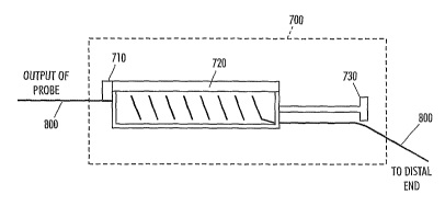
Figure 20 illustrates a further embodiment of the present invention wherein a
guide
wire or catheter 800 is connected to a Balun 700. The Balun 700 includes a
variable capacitor
710, a copper foil 720, and a non-conductive tuning bolt 730. The Balun 700 is
further
connected to the output of the probe 800
The Balun 700 adjusts its characteristic impedance by increasing or decreasing
the
number wire coils are found within the copper foil 720. The combination of the
coils and the
copper foil 720 forms a variable capacitor, having it impedance determined by
the change in
3o the surface area of the coils positioned opposite of the copper foil 720.
As more coils are
introduced into the volume created by the copper foil 720, the capacitance of
this combination
increases. Moreover, as fewer coils are introduced into the volume created by
the copper foil
720, the capacitance of this combination decreases. Thus, the capacitance of
the Balun 700 is
adjusted to create the unbalanced characteristic impedance.
Figure 21 illustrates another embodiment of the present invention wherein a
guide wire
or catheter 900 is electronically isolated by a voltage control unit to always
appear as an
-23
CA 02517771 2005-08-31
WO 2005/003790 PCT/US2004/020126
unbalanced line to any possible magnetic field that may be applied from a
magnetic resonance
imager unit (not shown). As current begins to flow due to the changing
magnetic fields from
the magnetic resonance imaging, a tapped voltage from a voltage-controlled
oscillator in the
magnetic resonance imaging unit is applied across terminals X1 and X2 of the
~joltage control
unit.
According to the concepts of the present invention, to automatically maintain
an
unbalanced characteristic impedance at the distal end of the guide wire or
catheter 900, a
capacitance unbalanced balun unit 7000, located within the voltage control
unit, is connected
through a variable inductor 910 to the proximal end of the guide wire or
catheter 900. In other
1o words, the voltage control unit containing the capacitance unbalanced balun
unit 7000 is
outside the body at the proximal end of the guide wire or catheter 900. By
having the
capacitance unbalanced bakun unit 7000 and variable inductor 910 outside the
body, the
varying of the reactance (XO) of the guide wire or catheter 900 can be readily
adjusted and
automatically controlled by the voltage control unit circuit's reactance to
the tapped voltage
from the voltage-controlled oscillator in the magnetic resonance imaging unit
as it is applied
across Xl and X2 for any instance of time from time zero (TO) or instantiation
of the magnetic
resonance imaging radio-frequency pulses.
The capacitance unbalanced bakun unit 7000 includes two non-magnetic trimmer
capacitors C1 and C2 connected in parallel with LC circuits (L1,C3) and
(L2,C4),
2o respectively, setting up a simplified dual T network that is effectively in
series ~rith the guide
«~ire or catheter 900. Ii is noted that one end of the simplified dual T
network is comzected to
neutral H1 and the other end is connected to a continuously variable voltage
H2, based on
inputs to the circuit from the voltage-controlled oscillator in the magnetic
resonance imaging
unit at Xl and X2. The reactance (XO) of the LC circuits in the T network is
automatically
adjusted to create the desired unbalanced characteristic impedance.
More specifically, the T network L1, C1, C3 and L2, C2, C4 respectively, may
be used
for both matching and unznatching characteristic impedance of the guide wire
or catheter 900
and to provide a certain amount of balancing or unbalancing for the guide wire
or catheter 900
by varying the circuit's capacitive or inductive reactance (XO).
3o In this example, as the voltage from the voltage-controlled oscillator in
the magnetic
resonance imaging unit is provided to the voltage control unit (X1 X2), the
two non-magnetic
trimmer capacitors Cl and C2, connected in parallel with LC circuits, (L1,C3)
and (L2,C4),
lift the voltage on the guide wire or catheter 900 from ground to an
unbalanced state with
respect to the radio-frequency pulse applied by the magnetic resonance imaging
unit. The
reactance of the T netZVOrI: and its LC circuits, (L1,C3) and (L2,C4),
respectively, cause the
guide wire or catheter 900 to become asymmetric and unbalanced, automatically
breaking
-24
CA 02517771 2005-08-31
WO 2005/003790 PCT/US2004/020126
dorm the reactance to ensure that resonance for the guide wire or catheter 900
is never present,
thus reducing the chances of thermal injury at the distal end of the guide
wire or catheter 900
due to heating from induced voltages.
While various elamples and embodiments of the present invention have been
shown
and described, it will be appreciated by those skilled in the an that the
spirit and scope of the
present invention are not limited to the specific description and drawings
herein, but extend to
various modifications and changes.
-25-