Note: Descriptions are shown in the official language in which they were submitted.
CA 02518072 2005-09-02
WO 2004/083923 PCT/GB2004/001122
1
Optical Wavelength Division Multiplexer/Demultiplexer Device.
This invention relates to an optical wavelength division
multiplexer/demultiplexer
device, and to various devices incorporating such a wavelength division
multiplexer/demultiplexer device.
Optical fibre based telecommunication and data networks are commonplace. In
order to maximise the bandwidth of each optical fibre link, it is known to
transmit a
number of data carrying light beams of slightly different wavelength through a
single optical fibre cable. Typically each wavelength is generated separately,
for
example by a solid state laser, and modulated to carry the required digital
data
signal. The different wavelength channels are then combined in a multiplexer
before
being coupled into the optical fibre.
To extract each of the various light beams of different wavelength from a
combined
beam, a demultiplexer is used. The signal carried by each beam can thus be
separately detected allowing the digital data to be extracted, or each beam
can be
separately acted upon (e.g. amplified, attenuated, re-routed etc). Typically a
demultiplexer is identical in construction to a multiplexer; the demultiplexer
simply
being a multiplexer device operated in reverse.
One known type of wavelength division multiplexer comprises a cascade of
spectral
filters. Each spectral filter has different transmission/reflection
characteristics and
will only transmit light within a given wavelength band. Multiple wavelength
component signals are built up by reflecting light comprising wavelengths
outside
the transmission band from one side of a filter, whilst also passing light
within the
transmission band through the filter in a direction such that it coincides
with the
direction of propagation of the reflected light. In this manner, optical
signals
comprising multiple wavelength components can be constructed. Typically, the
components forming the multiplexer are aligned with respect to one another in
adjustable mounts or are actively aligned prior to fixing. Light then
propagates
between the components in free space.
CA 02518072 2012-02-08
29756-301
2
A number of disadvantages are associated with known multiplexer devices of the
type described above. For example, the spectral properties of thin film
filters are
inherently strongly dependent on the angle of incidence of light. Therefore,
the filters
require precise angular alignment with respect to the incident light or their
wavelength
dependent transmission/reflection characteristics will be degraded resulting
in optical
leakage. In the case of a multiplexer, angular alignment of the filters is
also important
to ensure that the propagation paths of different wavelength signals are truly
co-
incident after combination to enable efficient coupling into any output
optical fibre.
The compounded effect of angular misalignment down the filter cascade greatly
increases the filter angular alignment accuracy that is required. To achieve
the
required filter alignment accuracy, the optical components of a multiplexer
device are
typically adjusted during assembly to ensure the alignment is optimised; this
can
prove time consuming, complex and costly. In addition, the free space
propagation of
light can lead to beam diffraction effects that reduce the overall optical
efficiency of
the device. Mechanical shock and/or thermal effects can also lead to
degradation of
component alignment over time.
Some embodiments of the present invention may mitigate at least some of the
disadvantages described above.
According to a first aspect of the present invention, an optical wavelength
division
multiplexer/demultiplexer device comprises a substrate having a plurality of
wavelength selecting filters, said filters being arranged to provide
conversion between
a combined beam comprising a plurality of wavelength channels and a plurality
of
separate beams each comprising a subset of said plurality of wavelength
channels,
characterised in that hollow core waveguides are formed in said substrate to
guide
light between the wavelength selecting filters.
The guiding of light within hollow core waveguides is advantageous as it may
reduce
beam divergence and cross-talk effects within the device. Some embodiments of
the
present invention may thus provide a multiplexer or demultiplexer having a
greater
optical efficiency than
CA 02518072 2012-02-08
29756-301
3
known devices in which light propagates between wavelength selecting filters
in free
space. The guiding of light though the device may also ensure that beam
diffraction
effects do not reduce the efficiency with which light can be coupled into
optical
fibres as it exits the device.
The term wavelength channel as used herein means a range of wavelengths within
a
defined wavelength band. Typically; a wavelength channel would be a single
wavelength output (e.g. from a solid state laser) having a certain line width.
A
number of standard wavelength bands are defined by the International
Telecommunications Union (ITU). For example, ITU dense wavelength division
multiplexing (DWDM) systems use light signals having a 100GHz frequency
separation.
The device, when acting as a demultiplexer, thus splits a beam comprising a
set of
wavelength channels into a plurality of beams each comprising a subset of
these
wavelength channels. 'Each separate beam may comprise only a single wavelength
channel, or it may comprise two or more wavelength =channels. Similarly, when
acting as a multiplexer, the device combines separate beams (each of which may
comprises one or more wavelength channels) to form a combined beam that
includes
all the wavelength channels of the separate beams.
It should be noted that when hollow core optical waveguide structures are
produced,
the hollow core is likely to fill with air. However, this should be seen in-no
way as
limiting the scope of this invention. The hollow core may contain any fluid
(for
example a liquid or an inert gas such as nitrogen) or be a vacuum. The term
hollow
core simply means a core which is absent any solid material. Furthermore, the
terms
"light" and "optical" are used herein to refer to any electromagnetic
radiation having
a wavelength from the deep ultraviolet to the far infra-red.
Conveniently, each wavelength selecting filter transmits a single wavelength
channel. Alternatively, each wavelength selecting filter advantageously
reflects a
CA 02518072 2005-09-02
WO 2004/083923 PCT/GB2004/001122
4
single wavelength channel. A combination of transmitting and reflecting
filters may
also be employed.
Advantageously, the wavelength selecting filters comprise thin film optical
filters.
For example, multi-layer or etalon thin film optical filters. A typical thin
film filter
will have about a 0.1nm shift in its central band-pass wavelength if mis-
aligned by
10.
Preferably, the substrate additionally comprises a plurality of alignment
slots
arranged to receive, in alignment, said optical filters. Alignment slots may
be
formed in the substrate and appropriately shaped to receive, in alignment, the
wavelength selecting filters. The alignment slots may be deeper/shallower
and/or
wider/narrower than the hollow core optical waveguides as required.
Fabricating alignment slots with sufficient accuracy to align the filter (i.e.
so that the
alignment slot is arranged to receive the filter in alignment) is especially
advantageous. In such a case, placing the filter in the alignment slot
inherently
aligns the filter with respect to the hollow core waveguide, and hence
accurately
determines the angle of incidence of light on the filter. A separate filter
alignment or
adjustment step is therefore not required. Conventional pick and place
techniques of
the type used in the manufacture of electronic circuits and the like could be
used to
place the filters in the appropriate alignment slots.
The alignment slots may also advantageously comprise micro-electromechanical
system (MEMS) spring clips or clamps to hold the filters or to push the filter
into
engagement with a reference surface.
Alternatively, pick and place techniques may be used to provide the necessary
alignment. For example, a component could be accurately aligned during
placement
and then fixed (e.g. glued) to remain in alignment.
CA 02518072 2005-09-02
WO 2004/083923 PCT/GB2004/001122
Preferably the substrate in which said hollow core waveguides and any
alignment
slots are formed comprises semiconductor material. Semiconductor substrates,
such
as Silicon, can be etched with good accuracy using micro-fabrication
techniques
such as deep reactive ion etching. The substrate may advantageously comprise a
5 multiple layer wafer; for example silcon on germanium (Site), silicon on
sapphire,
silicon-on-insulator (SOI) or silicon-on-glass. A person skilled in the art
would
recognise that micro-fabrication techniques typically involve a lithography
step to
define a pattern, followed by an etch step to transform the pattern in to one
or more
layers on, or in, the substrate material. The lithography step may comprise
photolithography, x-ray or e-beam lithography. The etch step may be performed
using ion beam milling, a chemical etch, a dry plasma etch or a deep dry etch
(also
termed deep silicon etch). Micro-fabrication techniques of this type are also
compatible with various layer deposition techniques such as sputtering, CVD
and
electro or electro-less plating.
Although substrates that comprise semiconductor material can advantageously be
used, the device could also be formed on a variety of alternative substrate.
The
substrate could advantageously be silicon oxide based; for example formed from
quartz, silica or glass. Substrates could also be embossed, or patterns could
be
lithographically defined in polymer layers. From a manufacturing perspective,
it can
be advantageous to use batch micro-fabrication techniques.
Advantageously, a base portion and a lid portion are provided to define said
hollow
core waveguide. Such an arrangement is described in more detail in PCT patent
application GB2003/000331 and provides a convenient way to manufacture the
device.
Conveniently at least one further hollow core waveguide is provided in the
substrate
to guide said combined beam and/or said plurality of beams each comprising a
subset of said plurality of wavelength channels to/from said plurality of
wavelength
selecting filters.
CA 02518072 2005-09-02
WO 2004/083923 PCT/GB2004/001122
6
Advantageously at least one optical fibre alignment slot is provided in said
substrate,
said optical fibre alignment slot being arranged to receive an optical fibre
in
alignment thereby enabling light to be coupled between said optical fibre and
said at
least one further hollow core waveguide.
In other words, optical fibre alignment slots may be formed in the substrate
to
receive optical fibres carrying beams to, or from, the hollow core waveguides
of the
device. In the case of solid core fibres, stepped optical fibre alignment
slots may be
provided to hold both the buffer layer and the cladding. The alignment of the
core of
a hollow core optical fibre with the hollow core waveguide of the device may
also
be achieved; for example by clamping the optical fibre cladding in a alignment
slot.
The use of hollow core optical fibres would be especially advantageous as the
air
core to air core connection would be free from any unwanted reflections.
To provide efficient coupling between the core of an optical fibre and a
hollow core
waveguide of the device, the cross-section of the hollow core waveguide should
be
appropriate for the cross-section of the optical fibre core. In the case of
solid core
fibres, leakage into the cladding means that the width of the mode carried by
the
fibre is actually greater than the core diameter; for example typically the 10
m solid
core of a single mode glass fibre has a total field width of around 14 m
diameter.
Fibre ends of solid core fibres may be anti-reflection coated.
If the mode width of the fibre is different to that of the hollow core
waveguide,
mode matching means such as lenses (e.g. ball or GRIN rod etc) can be
conveniently
used to couple light between the at least one optical fibre and the at least
one further
hollow core waveguide. Alternatively, lensed fibres could be used which would
remove the requirement for separate lenses.
Preferably, at least one of the hollow core waveguides comprise one or more
hybrid
or monolithic reflective elements. The provision of reflective elements
enables the
hollow core waveguides to be formed from a number of waveguide sections which
are angled to each other. This enables, for example, beams to be guided
through a
CA 02518072 2005-09-02
WO 2004/083923 PCT/GB2004/001122
7
90 angle. The provision of such elements thus allows more compact optical
circuits
to be provided.
Advantageously, at least some of the internal surface of the hollow core
waveguides
carry a reflective coating. Conveniently, the reflective coating is a layer of
metal
such as gold, silver or copper. Metals will exhibit a suitably low refractive
index
over a wavelength range that is governed by the physical properties of the
metal;
standard text books such as "the handbook of optical constants" by E. D.
Palik,
Academic Press, London, 1998, provide accurate data on the wavelength
dependent
refractive indices of various materials. In particular, gold has a refractive
index less
than that of air at wavelengths within the range of around 500nm to 2.2 m;
this
encompasses wavelengths within the important telecommunications band of
1400nm to 1600nm. Copper exhibits a refractive index less than unity over the
wavelength range of 560nm to 2200nm, whilst silver has similar refractive
index
properties over a wavelength range of 320nm to 2480nm.
A layer of metal may be deposited using a variety of techniques known to those
skilled in the art. These techniques include sputtering, evaporation, chemical
vapour
deposition (CVD) and (electro or electro-less) plating. CVD and plating
techniques
allow the metal layers to be deposited without significant direction dependent
thickness variations. Sputtering using a rotating sample and/or source would
also
provide even coverage. Plating techniques are especially advantageous as they
permit batch (i.e. multi-substrate parallel) processing to be undertaken.
A skilled person would recognise that adhesion layers and/or barrier diffusion
layers
could be deposited on the hollow core waveguide surfaces prior to depositing
the
layer of metal. For example, a layer of chrome or titanium could be provided
as an
adhesion layer prior to the deposition of gold. A diffusion barrier layer,
such as
platinum, may also be deposited on the adhesion layer prior to gold
deposition.
Alternatively, a combined adhesion and diffusion layer (such as titanium
nitride,
titanium tungsten alloy or an insulating layer) could be used.
CA 02518072 2005-09-02
WO 2004/083923 PCT/GB2004/001122
8
The reflective coating may also be provided by an all-dielectric, or a metal-
dielectric, stack. A person skilled in the art would recognise that the
optical
thickness of the dielectric layer(s) provides an interference effect that will
determine
the reflective properties of the coating. The dielectric material may be
deposited by
CVD or sputtering or reactive sputtering. Alternatively, a dielectric layer
could be
formed by chemical reaction with a deposited metal layer. For example, a layer
of
silver could be chemically reacted with a halide to produce a thin surface
layer of
silver halide.
In other words, the reflective coating may be provided by an all-dielectric,
or a
metal-dielectric, stack. Semiconductor-dielectric stacks could also be used. A
person
skilled in the art would recognise that the optical thickness of the
dielectric layer(s)
gives the required interference effects and thus determines the reflective
properties
of the coating. The reflective properties of the coating may also be
dependent, to
some extent, on the properties of the material in which the hollow core
waveguides
are formed. Hence, the material from which the waveguide is formed may also
form
a base layer, and be a part of, any such multiple layer dielectric stack.
Conveniently, the hollow core waveguides are dimensioned to support
fundamental
mode propagation or alternatively to support multi-mode propagation.
If multi-mode hollow "core wave guide structures are provided, the device can
be
dimensioned to allow the re-imaging effect to be exploited. The re-imaging
phenomena, and details concerning calculation of the re-imaging distance for a
given waveguide, are described in more detail below. In short, the re-imaging
effect
provides a replication of an input field a certain distance from the injection
of such a
field into a multi-mode waveguide. Arranging the device so that all the path
lengths
through the device are multiples of this re-imaging length enables the input
field of
an input optical fibre to be replicated at any of the optical outputs. This
allow
efficient coupling of light into an output optical fibre.
CA 02518072 2005-09-02
WO 2004/083923 PCT/GB2004/001122
9
Advantageously, portions of the one or more hollow core optical waveguides
have a
substantially rectangular (which herein shall include square) cross-section. A
square,
or almost square, cross-section hollow core waveguide provides a waveguide in
which the losses are substantially polarisation independent and is preferred
when the
polarisation state of the light is unknown or varying. Dimensioning the
waveguide to
have a depth greater than its width, or vice versa, increases polarisation
dependent
losses, but may be advantageous when the polarisation state of light
propagating
through the waveguide is known.
Although rectangular cross-section waveguides are convenient, many alternative
waveguide shapes could be employed. For example, circular, elliptical or v-
shaped
waveguides could be provided.
Conveniently, the combined beam comprises at least three, four, eight,
sixteen,
thirty-two, sixty-four or one hundred and twenty eight wavelength channels.
According to a second aspect of the invention, an optical device comprises a
demultiplexer stage comprising a device according to the first aspect of the
invention that is arranged to receive a combined beam comprising a plurality
of
wavelength channels and to separate said combined beam into a plurality of
beams
each comprising a single wavelength channel, and a multiplexer stage
comprising a
device according to the first aspect of the invention that is arranged to
receive a
plurality of beams each comprising a single wavelength channel and to combine
said
plurality of beams to produce a combined beam comprising a plurality of
wavelength channels, wherein one or more of the plurality of beams produced by
the
demultiplexer stage are routed to the multiplexer stage via an optical
processing
means.
The use of a multiplexer and demultiplexer with an intermediate optical
processing
stage provides a device that can be used for extracting and acting separately
on one
or more wavelength channels in a combined beam that has a plurality of
wavelength
channels. The optical processing means may be formed in the substrate used to
CA 02518072 2012-02-08
29756-301
provide the multiplexer and demultiplexer stages, and may conveniently
comprise
components connected by hollow core optical wavegc ides. Forming the whole of
the
optical device in a common substrate reduces manufacturing complexity and
cost.
5 Conveniently, the optical processing means comprise at least one optical
amplifier,
for example an erbium doped fibre amplifier (EDFA). In this way the power of
one
or more individual wavelength channels could be increased; for example so that
the
device has a net zero optical loss. It would be appreciated that attenuators
(e.g.
variable optical attenuators) could be provided to reduce optical power of a
channel
10 if required.
Advantageously, the optical processing means comprise an optical routing means
thereby enabling the device to be used as an optical router. The optical
routing
means may be of a fixed configuration (thereby making the optical router "hard-
wire(f") or it may be re-configurable.
One or more additional wavelength channels may advantageously be received by
said optical routing means, said optical routing means being arranged to route
at
least some of said additional wavelength channels to said multiplexer stage.
In this
way, channels may be added to and/or dropped from a combined beam. Channels
dropped from a combined beam may subsequently be coupled into a second
combined beam. Complex routing devices can thus be constructed using a single
substrate.
The optical routing means may advantageously comprise a matrix switch. For
example, a two dimensional matrix switch of the type described in WO
2004/083916
may be used.
Conveniently, the matrix switch comprises an array of micro-electro-mechanical
systems (MEMS) activated components. Herein, MEMS is taken to include micro-
machined elements, micro-systems technology, micro-robotics and micro-
CA 02518072 2012-02-08
29756-301
11
engineering and the like. The MEMS component may advantageously comprise an
electro-thermal actuation mechanism (e.g. a bent beam arrangement) to provide
large
throw (e.g. 5-100 m full scale deflection) actuation. Alternative actuation
mechanisms
such as electromagnetic, electrostatic (e.g comb drive), bimorph or
piezoelectric may
also be used. More detail on MEMS device actuation technologies and the
associated
fabrication techniques can be found in "Fundamental of Microfabrication" by
Marc
Madou, published by CRC Press (Boca Raton) in 1997; ISBN 0-8493-9451-1.
According to a third aspect of the invention, a substrate for an optical
wavelength division
multiplexer/demultiplexer device comprises a plurality of alignment slots for
receiving a
plurality of wavelength selecting filters and hollow core waveguides to guide
light
between said alignment slots wherein the arrangement provides, when
appropriate
wavelength selecting filters are located in said alignment slots, conversion
between a
combined beam comprising a plurality of wavelength channels and a plurality of
beams
comprising a single wavelength channel.
Some embodiments of the invention will now be described, by way of example
only, with
reference to the following drawings in which;
Figure 1 shows a multiplexer of an embodiment of the present invention,
Figure 2 shows part of a further multiplexer of an embodiment of the present
invention,
and
Figure 3 shows an add/drop multiplexer device of an embodiment of the present
invention.
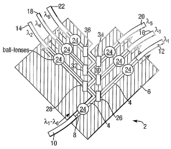
Referring to figure 1, a multiplexer 2 according to an embodiment of the
present invention
is shown. The multiplexer 2 comprises a hollow core optical waveguide
structure 4
having a rectangular cross-section formed in a silicon-on-insulator (SOI)
substrate 6 by
deep reactive ion etching. The multiplexer is arranged to receive a combined
light beam
8, comprising six component light beams of wavelength a,, to X6, from a single
mode
input optical fibre 10. A first output fibre 12, a second output fibre 14, a
third output
CA 02518072 2005-09-02
WO 2004/083923 PCT/GB2004/001122
12
fibre 16, a fourth output fibre 18, a fifth output fibre 20 and a sixth output
fibre 22
are provided to receive the six output beams having wavelengths X1 to X6
respectively. Ball lenses 24 are also provided to couple light between the
hollow
waveguide structure 4 and the input fibre 10 and each of the output fibres 12
to 22.
The substrate also comprises alignment slots in which a first filter 26, a
second filter
28, a third filter 30, a fourth filter 32, a fifth filter 34 and a sixth
filter 36 are located.
The first to sixth filters 26 to 36 are thin film filters having spectral
characteristics
that permit the transmission of light of wavelengths X1 to X6 respectively;
any
wavelength outside the specified filter wavelength being substantially
reflected by
the filter.
In use, the combined light beam 8 received from the input fibre 10 is coupled
into
the hollow core optical waveguide structure 4 and directed to the first filter
26. The
first filter 26 transmits light having the wavelength X1 and reflects all
other
wavelengths of light (i.e. the beams of wavelength X2 to X6). The light beam
component X1 is then guided, and coupled into, the first output fibre 12
whilst the
remaining components of the combined light beam (i.e. X2 to X6) are guided to
the
second filter 28. The second filter 28 transmits light having the wavelength
X2 and
reflects all other wavelengths (i.e. X3 to X6). The light beam component X2 is
then
guided, and coupled into, the second output fibre 14 whilst the remaining
components of the combined light beam (i.e. X3 to X6) are guided to the third
filter
30. This selective transmission/reflection is repeated for the fourth, fifth
and sixth
filters and results in light beams of wavelength X1 to X6 being coupled in to
the first
to sixth output fibres 12-22 respectively.
As described above, the provision of the hollow core waveguide structure
reduces
optical losses that are associated with free space propagation. The hollow
core
waveguide structure also ensures the combined light beam propagates along a
common optical path. Furthermore, defining alignment slots in the substrate
for the
spectral filters using the same process used to form the hollow core waveguide
CA 02518072 2005-09-02
WO 2004/083923 PCT/GB2004/001122
13
ensures that the filters are accurately aligned (e.g. at 45 ) with respect to
the
direction of light propagation in the waveguide; this maximises the efficiency
of the
filters.
It should be noted that the device described above is strictly operating as a
demultiplexer. However, the device could equally be operated in reverse to
combine
six light beams of different wavelength to form a combined light beam.
The device described with reference to figure 1 thus provides a compact
multiplexer
realisation. However, in some circumstances it is useful for the optical
fibres
carrying the single component beams to be laterally separated along one side
of the
multiplexer device. Figure 2 illustrate an implementation of such a
configuration.
Referring to figure 2, a portion of an alternative multiplexer 50 according to
the
present invention is shown. In common with the device described with reference
to
figure 1, the multiplexer 50 is arranged to receive a combined light beam 8,
comprising six component light beams of wavelength Xi to X6, from a single
mode
input optical fibre 10. A first output fibre 12, a second output fibre 14, a
third output
fibre 16, and fourth to sixth output fibres (not shown) are also provided to
receive
the six separated output beams having wavelengths X to X6 respectively. Ball
lenses
24 are provided to couple light -between the hollow waveguide structure 4 and
the
input fibre 10 and each of the output fibres. The substrate 6 in which the
multiplexer
is formed also comprises alignment slots in which a first filter 26, a second
filter 28,
a third filter 30 and fourth to sixth filters (not shown) are located.
The optical path within the multiplexer 50 differs from that shown in figure 1
so that
each of the output fibres can be laterally displaced along a common axis. In
order to
provide such a configuration, mirrors 52 are located within the waveguide
structure
in-between each of the filters to direct the combined beam through a ninety
degree
angle. In this way, the required angle of incidence of light on the filters
(45 in this
case) can be retained.
CA 02518072 2005-09-02
WO 2004/083923 PCT/GB2004/001122
14
Figure 2 illustrates just one possible modification to the hollow core
waveguide
structure of the multiplexer. A skilled person would appreciate that numerous
adjustments to the structure would be possible. For example, the hollow core
waveguide between filters could be routed through any angle; this could be
achieved
not only by reflection from mirrored surfaces, but in a variety of ways such
as
providing curved hollow core waveguide structures.
Referring to figure 3, a routing device 100 is shown that incorporates a
demultiplexer/multiplexer arrangement to provide a re-configurable optical add-
drop
16 multiplexer (ROADM). The routing device 100 includes a demultiplexer stage
102
and a multiplexer stage 104. An intermediate optical switching stage 106 is
also
provided between the demultiplexer and multiplexer stages.
The demultiplexer stage 102 comprises a three-way demultiplexer device. The
demultiplexer comprises a first filter 26, a second filter 28, a third filter
30 and a pair
of mirrors 52. The filters and mirrors are held in alignment slots formed in a
silicon
substrate, and are inter-connected by hollow core waveguides in the manner
described with reference to figure 2 above. An input fibre 108 is also
provided to
couple a three component (Xi-X3) light beam into the demultiplexer stage. The
three
spatially separated component beams are output from the stage via three
separate
hollow core optical waveguides.
The multiplexer stage 104 comprises a three-way multiplexer device. It
includes a
first filter 26, a second filter. 28, a third filter 30 and two mirrors 52.
The filters and
mirrors are held in alignment slots formed in a silicon substrate, and are
inter-
connected by hollow core optical waveguides in the manner described with
reference to figure 2 above. Each of the three waveguides carrying a component
beam from the demultiplexer stage 102 are optically coupled, via the
intermediate
stage, to a corresponding input waveguide of the multiplexer stage 104. A
first
output fibre 109 is also provided to receive the combined beam produced by the
multiplexer stage.
CA 02518072 2005-09-02
WO 2004/083923 PCT/GB2004/001122
The intermediate optical switching stage 106 provides the add/drop
functionality,
and comprises a first feed hollow core waveguide 114, a second feed hollow
core
waveguide 116 and a third feed hollow core waveguide 118. Each of the hollow
core
feed waveguides are arranged to orthogonally intersect the hollow core
waveguides
5 guiding light from the demultiplexer stage 102 to the multiplexer stage 104.
The
intermediate optical switching stage 106 also comprises second, third and
fourth
input fibes (120, 122 and 124) connected to one end of each of the first,
second and
third feed hollow core waveguides respectively. The second end of each feed
waveguide is also connected to second, third and fourth output fibes (126, 128
and
10 130) respectively. All the optical fibres are coupled to the hollow core
waveguide
via ball lenses 24.
A first reflective switch 132 is located in the feed optical waveguide 114 at
the point
at which it intersects the waveguide that is arranged to carry light of
wavelength X
'15 from the demultiplexer stage to the multiplexer stage. A second reflective
switch
134 is located in the second feed waveguide 116 at the point where it
intersects the
waveguide that is arranged to carry light of wavelength X2 from the
demultiplexer
stage to the multiplexer stage. A third reflective switch 136 is located in
the third
feed waveguide 118 at the point where it intersects the waveguide that is
arranged to
carry light of wavelength X3 from the demultiplexer stage to the multiplexer
stage.
Each reflective switch is angled at 45 to the propagation direction of light
in the
waveguides. The reflective element is reflective on both of its surfaces.
The reflective switches may comprise any type of MEMS actuated switch; e.g.
pop-
up mirrors or moveable reflective shutters. In place of switches having two
reflective
faces to provide the add and drop routing function, it would also be possible
to use
two separate switches to provide the drop and add functions. It should also be
noted
that although a re-configurable routing device is described herein, the switch
could
actually be permanently set in a single position; i.e. a hard wired or fixed
add/drop
function could be implemented.
CA 02518072 2005-09-02
WO 2004/083923 PCT/GB2004/001122
16
In use, a three component (X1-X3) combined light beam is coupled into the
demultiplexer stage from the first input optical fibre 108. The three
wavelength
components are spatially separated, and each is passed along a separate hollow
core
waveguide to the switching stage 106. If each of the reflective switches are
retracted,
light simply passes from the demultiplexer stage to the multiplexer stage and
is
recombined.
However, activation of a reflective switch causes the relevant wavelength
channel
from the first input optical fibre 108 to be re-routed to the second, third or
fourth
output fibre as appropriate. In place of this dropped wavelength channel, the
wavelength channel from the second, third or fourth input fibre, as
appropriate, is
added to the combined beam. In this way, the device can exchange any of the
light
beams of wavelength X1 to X3 in the combined beam with the light carried by
the
second, third and fourth optical fibres 120, 122 and 124 respectively.
The intermediate switching stage of the device described with reference to
figure 3
provides a simple means of adding and/or dropping wavelength components of a
multiple component beam. A skilled person would appreciate how devices could
be
provided in accordance with the teachings contained herein to provide more
complex add/drop functions. For example, multiple demultiplexer and
multiplexer
stages could be used in combination with a high complexity optical matrix
switch to
provide higher order add/drop functions.
The intermediate switching stage may also comprise semiconductor lasers and/or
modulators to produce the replacement beams carried by the second, third or
fourth
input fibres 120, 122 and 124. Similarly, detectors could be provided to
convert the
optical signals of the second, third and fourth output fibres into electrical
outputs.
Various amplifier and attenuator elements could also be added; for example to
make
the device a zero-loss component.
Any multiplexer/demultiplexer devices of the type described above may be
dimensioned to exploit the so-called "re-imaging" phenomena that is found with
CA 02518072 2005-09-02
WO 2004/083923 PCT/GB2004/001122
17
multi-mode waveguides. The re-imaging effect is described in more detail
elsewhere; for example see PCT patent application GB2003/000331. In short, it
has
been found that multi-mode waveguides (in particular those with a rectangular
cross-
section) can be designed to provide re-imaging of symmetric, anti-symmetric or
asymmetric optical fields of a given wavelength by designing the length of the
waveguide to have an appropriate relationship to its width and depth. In other
words,
the Gaussian input profile of an input beam is re-imaged (i.e. reproduced)
after
propagating a certain distance along a given waveguide. This effect also gives
rise to
beam replication; i.e. multiple images of the beam being formed at distances
shorter
than the re-imaging length. These effects have been described previously in
US5410625 and provides the basis for multi-mode interference (NMI) beam
splitting devices.
As an example, consider a symmetric field in a square sectioned waveguide.
This
will have a re-imaging length that is given by the square of the waveguide
width
over the wavelength of the propagating radiation. Re-imaging of the symmetric
field
occurs at the re-imaging length and multiples of the re-imaging length. For
the case
of a 50.0 m wide hollow waveguide and 1.55 m radiation, the re-imaging length
is
thus 1.613 mm. The symmetric field would be re-imaged at this length and also
at
integer multiples of this length, i.e. 3.23 mm, 4.84 mm etc. For example, a
TEM00
Gaussian input beam from a single mode optical fibre could be re-imaged at
distances of 1.613 mm.
Alternatively, for the case of an asymmetric optical field, re-imaging occurs
at eight
times the length required for symmetric field re-imaging, i.e. at 12.09 mm for
a
50.0 m wide hollow waveguide. A mirror image of the asymmetric field is also
formed at half this length i.e. at 6.05 mm. In particular, offsetting the
input from the
centre line of the multimode region provides an asymmetric input that is re-
imaged
at pre-determined distances along the guide at an equivalent offset on either
side of
the centre line.
CA 02518072 2005-09-02
WO 2004/083923 PCT/GB2004/001122
18
In the case of a rectangular waveguide where the depth and width of the
waveguide
are substantially different, the re-imaging lengths associated with the two
waveguide cross-sectional dimensions (e.g. depth and width) are themselves
different. However, by arranging that the relationship between the dimensions
of the
rectangular hollow waveguide is such that re-imaging is produced at identical
lengths for the particular width and depth, any field can be re-imaged. Thus,
a
symmetric field can be re-imaged in a hollow rectangular waveguide by
arranging
that the re-imaging lengths associated with axes of width wl and w2 to be
identical.
The optical path length from an input fibre to the associated output fibre(s)
in a
device described above could thus be arranged to correspond to the re-imaging
distance (or a multiple thereof). Furthermore, the reflective switches in the
device
described with reference to figure 3 above could be arranged to lie at re-
imaging
points.
Using an arrangement that employs the re-imaging effect has the advantage that
collimating means (e.g. ball lenses 24) are not required in order to couple
light
between the hollow core waveguides and the associated optical fibres.
Furthermore,
placing each MEMS switch at a re-imaging distance further reduces the
acceptable
angular alignment tolerances of the MEMS components. The use of the re-imaging
effect also reduces diffraction losses where the waveguide has to be broken in
order
to facilitate the location of a moveable reflective element.
Finally, it should be noted that although light is incident on the spectral
filters
described with reference to the above figures at 45 this should not be seen
as
limiting the scope of the invention. The angle of the hollow core waveguides
with
respect to the spectral filters can be chosen to direct light to the filter at
the filter's
designed angle of incidence. Furthermore, it would be appreciated by the
skilled
person that the angle of incidence may be different for filters having
different
spectral characteristics.