Note: Descriptions are shown in the official language in which they were submitted.
CA 02518154 2005-09-O1
- 1 - 2004P03640US-RAI
Circuit arrangement for operating at least one high pressure
discharge lamp
Field of the invention
The present invention relates to a circuit arrangement for
operating at least one high-pressure discharge lamp having four
switches in a full bridge arrangement, a first and a second
switch forming the first half-bridge arm, and a third and a
fourth switch forming the second half-bridge arm, at least two
terminals for coupling the high pressure discharge lamp between
the midpoint of the first and of the second half-bridge arms,
at least one terminal for supplying the circuit arrangement
with a DC voltage signal, and a drive circuit for driving the
four switches, the drive circuit being designed to provide a
first drive signal for the switches of the first half-bridge
arm and a second drive signal for the switches of the second
half-bridge arm in such a way that the first and the second
drive signals are derived from a base signal whose clock pulse
is swept between a first and a second frequency, and in such a
way that the first and the second drive signals have a phase
difference which is modulated with a prescribeable third
frequency.
Background of the invention
Such a circuit arrangement is disclosed in DE 103 33 820.9 from
the same applicant as the present application. The disclosure
content of this application, particularly with regard to the
prior art described there as well as the statements on phase
modulation, is incorporated into the present application by
this reference. However, the circuit arrangement presented
there for carrying out a phase modulation is attended by very
high outlay on implementation that is reflected in the costs.
CA 02518154 2005-09-O1
- 2 - 2004P03640US-RAI
As is therefore known to the person skilled in the art, the
frequency of the base signal is selected such that said
frequency is between the first ~azimuthal resonant mode and the
first radial acoustic resonant mode of the lamp. Moreover, the
third frequency is selected such that the latter corresponds
approximately to the second longitudinal resonant frequency of
the lamp.
In relation to the prior art, reference may further be made to
US 2003/0102824 A1, which discloses a circuit arrangement for
the high-frequency operation - the carrier frequency being
between 400 and 600 kHz - of a high pressure discharge lamp. As
is known to the person skilled in the art, during operation of
a high pressure discharge lamp with a carrier frequency in this
frequency range there is no need to take any measure for arc
straightening. In DE 103 33 820.9, the sweeping of the carrier
frequency serves the purpose of arc straightening. In order to
prevent color segregation, in the abovementioned
US 2003/0102824 A1 a low-frequency signal of the order of
magnitude between 20 and 30 kHz and which corresponds to the
second longitudinal resonant frequency is used to switch to and
fro between two carrier frequencies. The frequency range used
in this publication for the carrier frequency is, however, not
desired in practice since it is attended by emission problems.
It would not be possible to implement an operation of the
circuit arrangement proposed in the abovementioned US document
with carrier frequencies in the range around 50 kHz, since the
required filter characteristic would be associated with a high
outlay on components given such a low frequency. The modulation
frequency is coupled to the carrier frequency in a fixed
fashion owing to the filter used and to the sweeping.
Summary of the invention
It is therefore the object of the present invention further to
improve the circuit arrangement disclosed in DE 103 33 820.9.
CA 02518154 2005-09-O1
- 3 - 2004P03640US-RAI
The present invention is based on the finding that the above
object can be achieved in a simple way when the drive circuit
is designed to switch to and fro by means of a switch between
derivatives of the base signal with a different phase shift. It
is possible by means of this measure to dispense with a
sinusoidal modulation signal that was required in
DE 103 338 820.9 and was therefore produced in the circuit
arrangement. The degree of amplitude modulation can be varied
in a simple way by the magnitude of the phase shift. The
boundary conditions are thereby set for implementing this
principle in a simple way by means of a microcontroller without
external wiring. By comparison with US 2003/0102824 A1, in the
case of the present invention the carrier frequency and the
third frequency used for modulation are not coupled to one
another, and so the additional measure for arc straightening,
that is to say the sweeping of the carrier frequency, can
easily be converted into a circuit arrangement according to the
invention. From the comparison with the known circuit
arrangements, the solution according to the invention is
distinguished by a reduction in complexity and a reduction in
the costs of implementation.
The control circuit is preferably designed to drive the in each
case two switches of a half-bridge arm with complementary
signals.
One category of embodiments is distinguished in that the drive
circuit has a switch which is designed to switch to and fro
between two representations of the base signal with a different
phase angle in time with the third frequency in order to derive
the second drive signal from the base signal. By comparison
with the base signal, the first control signal then has a fixed
phase shift, in the simplest case a phase shift of 0°. This
constitutes the possibility of implementation with the lowest
outlay.
CA 02518154 2005-09-O1
- 4 - 2004P03640US-RAI
It is further preferred to invert the first drive signal in
relation to the base signal. It is possible thereby to select
the operating point, that is to say if the first drive signal
is inverted, the power consumption of the lamp drops with a
rising phase shift. Conversely, in the case of a non-inverted
first drive signal the power consumption in the lamp rises with
rising phase shift.
The phase shift between the base signal and the control signal
can be used for the purpose of power setting.
A second category of embodiments is distinguished in that the
drive circuit has two switches, the first switch being designed
to switch to and fro between two representations of the base
signal with a different phase angle in time with the third
frequency in order to derive the first drive signal from the
base signal, and the second switch being designed to switch to
and fro between two representations of the base signal with a
different phase angle in time with the third frequency in order
to derive the second drive signal from the base signal. The
power setting can be undertaken here by means of the relative
phase angle of the representations of the base signal, between
which there is switching to and fro in each case.
It is preferred, furthermore, that the phase shift between the
first and the second drive signals is performed in a dual
alternating fashion, the base phase shift being prescribeable,
as mentioned, for the purpose of power setting.
In a preferred fashion, the sweep frequency is between 50 Hz
and 500 Hz, preferably between 80 Hz and 200 Hz. In a preferred
fashion, the frequency of the base signal is below 150 kHz,
preferably between 35 and 70 kHz or between 80 and 120 kHz. It
is furthermore preferred to sweep the frequency of the base
signal between substantially 40 kHz +/- loo and 60 kHz +/- 100.
In a preferred fashion, the third frequency is below 50 kHz,
preferably between 20 and 35 kHz.
CA 02518154 2005-09-O1
- 5 - 2004P03640US-RAI
The drive circuit can be implemented both by means of hardware
and software and in combinations of hardware and software.
Further advantageous embodiments emerge from the subclaims.
Brief description of the drawings
An exemplary embodiment will now be described in more detail
below with reference to the attached drawings, in which:
figure 1 shows a schematic of a first part of a circuit
arrangement according to the invention;
figure 2 shows a schematic of a second part of a circuit
arrangement according to the invention;
figure 3 shows a schematic of the time profile of various
signals; and
figure 4 shows the time profile, measured from an exemplary
embodiment of a circuit arrangement according to the
invention, of the lamp voltage, as well as the
amplitude spectrum of the lamp voltage.
Detailed description of the invention
Figure 1 shows a first part of a circuit arrangement according
to the invention. Here, four switches Q1 to Qq are driven in a
full bridge arrangement via respective driver circuits 10, 12.
The signals provided at the output of the respective driver
circuits 10, 12 are complementary to one another. Coupled
between the midpoints Ml, M2 of the two half-bridge arms is an
LC circuit 14 to which a high pressure discharge lamp 16 is
connected. The circuit arrangement is supplied with a DC
voltage signal U~, for example 400 V DC. The driver circuit 10
is driven with a signal A and the driver circuit 12 with a
CA 02518154 2005-09-O1
- 6 - 2004P03640US-RAI
signal B, the generation and time profile of which will be
examined in more detail with reference to figures 2 and 3.
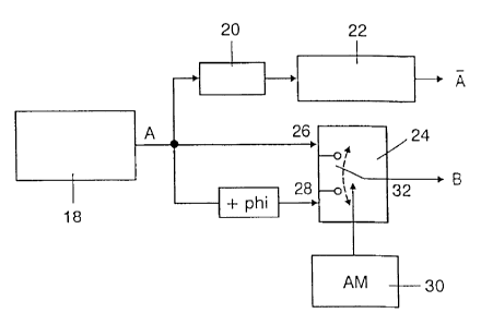
In accordance with figure 2, in order to generate the signals
A and B an oscillator device 18 firstly provides a square-wave
signal A that is swept between 40 kHz and 60 kHz and whose time
profile is to be seen in figure 3 as curve c) . This traverses
an inverter 20 and a unit 22 for power setting by varying the
phase shift in relation to the signal A. The signal A is
provided at the output of the unit 22. Moreover, the signal A
is applied to a first input 26 of a switching device 24 and to
a second input 28 of the switching device 24 as signal A + phi
in a variant displaced by the angle + phi. The device 30
effects switching to and fro between the inputs 26 and 28 of
the switching device 24 in time with a frequency fAM that is
between 20 and 35 kHz. The signal present at the input 26 or at
the input 28 is correspondingly alternatively provided at the
output 32 as signal B.
As mentioned, the time profile of the signal A is firstly to be
recognized in figure 3 as curve c). The curve b) shows the
profile inverted relative thereto, specifically the signal A.
Curve d) shows the profile of the signal A+phi, which is
displaced by + phi from the signal A. The curve a) shows the
profile of the switching signal AM, which determines at which
instant the signal A and at which instant the signal A + phi is
led to the output of the switching device 24 and is provided
there as signal B. The time profile of the signal B is
illustrated as curve e).
Figure 4 shows at the top the time profile of the lamp voltage
connected to the lamp 16. The envelope in which the switching
frequency f~,, is reproduced is well in evidence. Recognizable
therebelow is the amplitude spectrum, which reflects the
frequency ft of the signal A. The sidebands are arranged at a
spacing of +/- fpM from ft.