Note: Descriptions are shown in the official language in which they were submitted.
CA 02518396 2005-09-08
Internal reference: IRDM.094 NON-EP / IDC-040056
METHOD AND DEVICE FOR PROVIDING
ELECTRONIC CIRCUITRY ON A BACKPLATE
Background of the Invention
Field of the Invention
The field of the invention relates to microelectromechanical systems (MEMS).
More
specifically, the feld ofthe invention relates to interferometric modulator
based displays.
Descrption of the Related Technology
Display devices such as LCDs generally require electronic controlling
circuitry located
exterior to a protective package surrounding the display element. For example,
an LCD
comprises two sheets of glass surrounding a liquid crystal element.
Controlling an LCD typically
requires circuitry external to the package formed by the two sheets of glass.
Positioning such
controlling circuitry exterior to this protective package necessarily
increases either the footprint
or the height of the device.
Other types of displays are based on microelectromechanical systems (MEMS).
These
MEMS can include micro mechanical elements, actuators, and electronics.
Micromechanical
elements may be created using deposition, etching, and or other micromachining
processes that
etch away parts of substrates and/or deposited material layers or that add
layers to form electrical
and electromechanical devices. One type of MEMS device is called an
interferometric
modulator. An interferometric modulator may comprise a pair of conductive
plates, one or both
of which may be transparent and/or reflective in whole or part and capable of
relative motion
upon application of an appropriate electrical signal. One plate may comprise a
stationary layer
deposited on a substrate, the other plate may comprise a metallic membrane
separated from the
stationary layer by an air gap. Such devices have a wide range of
applications, and it would be
beneficial in the art to utilize and/or modify the characteristics of these
types of devices so that
their features can be exploited in improving existing products and creating
new products that
have not yet been developed.
Summary of Certain Embodiments
The system, method, and devices of the invention each have several aspects, no
single
one of which is solely responsible for its desirable attributes. Without
limiting the scope of this
invention, its more prominent features will now be discussed briefly. After
considering this
discussion, and particularly after reading the section entitled "Detailed
Description of Certain
CA 02518396 2005-09-08
Embodiments" one will understand how the features of this invention provide
advantages over
other display devices.
One embodiment of the invention is a display, wherein the display includes: a
transparent
substrate; an array of interferometric modulators comprising reflective
elements that are
configured to reflect light through said transparent substrate; a backplane
comprising a first
surface proximal to the array of interferometric modulators and comprising
electronic circuitry
fabricated on said first surface of the backplane, wherein the electronic
circuitry is configured to
control the movement of the reflective elements; and a plurality of electrical
connections
providing electronic communication between the electronic circuitry on the
backplane and the
array of interferometric modulators.
Yet another embodiment of the invention is a method of fabricating a display,
comprising: providing a transparent substrate comprising an array of
interferometric modulators
on a first surface of the transparent substrate, wherein said modulators
comprise reflective
elements; providing a backplate having a first surface; forming electronic
circuitry on the first
surface of the backplate, wherein the electronic circuitry is configured to
control the state said
reflective elements; and positioning the transparent substrate and the
backplate such that the first
surface of the transparent substrate is located proximal the first surface of
the backplate and the
electronic circuitry is placed in electrical connection with the array of
interferometric modulators.
Still another embodiment of the invention is a display made by the method of:
providing
a transparent substrate comprising an array of interferometric modulators on a
first surface of the
transparent substrate, wherein said modulators comprise reflective elements;
providing a
backplate having a first surface; forming electronic circuitry on the first
surface of the backplate,
wherein the electronic circuitry is configured to control the state said
reflective elements; and
positioning the transparent substrate and the backplate such that the first
surface of the
transparent substrate is located proximal the first surface of the backplate
and the electronic
circuitry is placed in electrical connection with the array of interferometric
modulators.
One additional embodiment of the invention is an electronic display that
includes:
transmitting means for transmitting light therethrough; modulating means for
modulating light
transmitted through the transmitting means; covering means comprising a first
surface proximal
to the modulating means and comprising electronic means fabricated on said
first surface,
wherein the electronic means is configured to control the movement of the
modulating means;
and providing means for providing electronic communication between the
electronic means and
the modulating means.
-2-
CA 02518396 2005-09-08
Brief Description of the Drawings
Figure 1 is an isometric view depicting a portion of one embodiment of an
interferometric modulator display in which a movable reflective layer of a
first interferometric
modulator is in a released position and a movable reflective layer of a second
interferometric
modulator is in an actuated position.
Figure 2 is a system block diagram illustrating one embodiment of an
electronic device
incorporating a 3x3 interferometric modulator display.
Figure 3 is a diagram of movable mirror position versus applied voltage for
one
exemplary embodiment of an interferometric modulator of Figure I .
Figure 4 is an illustration of a set of row and column voltages that may be
used to drive
an interferometric modulator display.
Figures SA and SB illustrate one exemplary timing diagram for row and column
signals
that may be used to write a frame of display data to the 3x3 interferometric
modulator display of
Figure 2.
Figure 6A is a cross section of the device of Figure I .
Figure 6B is a cross section of an alternative embodiment of an
interferometric
modulator.
Figure 6C is a cross section of another alternative embodiment of an
interferometric
modulator.
Figure 7 is a cross-sectional view of a basic package structure for an
interferometric
modulator-based display.
Figure 8 is a cross-sectional view of a package structure for an
interferometric modulator-
based display in which electronic components are located on the underside of
the backplate.
Figure 9 is a view of the underside of a backplate which provides physical
support for a
variety of electronic components.
Figure 10 is a cross-section of a backplate on which thin-film electronic
circuitry has
been fabricated.
Figure 11 is a cross-sectional view of a package structure for an
interferometric
modulator-based display having electronic circuitry fabricated on the
underside of the backplate.
Figure 12A is a cross-sectional view of an unassembled package structure for
an
interferometric modulator-based display having electronic circuitry fabricated
in a depression
area on the underside of the backplate, shown prior to thermocompression.
Figure 12B is a cross-sectional view of the package structure of Figure 12A,
shown
assembled and after thermocompression.
Figures 13A and 13B are system block diagrams illustrating an embodiment of a
visual
display device comprising a plurality of interferometric modulators.
-3-
CA 02518396 2005-09-08
Detailed Description of the Preferred Embodiment
An embodiment of the invention, as discussed in greater detail below, is an
interferometric modulator-based display wherein the backplate contains
electronic circuitry
fabricated on the interior side of the backplate. This electronic circuitry is
capable, among other
things, of controlling the state of the array of interferometric modulators.
This is useful, for
example, in order to provide the display driver circuit within the display
package. The
fabrication of the driver chip within the display package, and on the interior
side of the backplate
advantageously permits greater flexibility in the design of the electronic
circuitry. In addition,
such fabrication advantageously permits optimal use of space within the
display, permitting the
creation of a device which may be thinner and/or have a smaller footprint than
prior devices. The
fabrication of the electronic circuitry, rather than the use of existing
driver chips, may also result
in significant cost savings.
The following detailed description is directed to certain specific embodiments
of the
invention. However, the invention can be embodied in a multitude of different
ways. In this
description, reference is made to the drawings wherein like parts are
designated with like
numerals throughout. As will be apparent from the following description, the
invention may be
implemented in any device that is configured to display an image, whether in
motion (e.g., video)
or stationary (e.g., still image), and whether textual or pictorial. More
particularly, it is
contemplated that the invention may be implemented in or associated with a
variety of electronic
devices such as, but not limited to, mobile telephones, wireless devices,
personal data assistants
(PDAs), hand-held or portable computers, GPS receivers/navigators, cameras,
MP3 players,
camcorders, game consoles, wrist watches, clocks, calculators, television
monitors, flat panel
displays, computer monitors, auto displays (e.g., odometer display, etc.),
cockpit controls and/or
displays, display of camera views (e.g., display of a rear view camera in a
vehicle), electronic
photographs, electronic billboards or signs, projectors, architectural
structures, packaging, and
aesthetic structures (e.g., display of images on a piece of jewelry). MEMS
devices of similar
structure to those described herein can also be used in non-display
applications such as in
electronic switching devices.
One interferometric modulator display embodiment comprising an interferometric
MEMS display element is illustrated in Figure 1. In these devices, the pixels
are in either a
bright or dark state. In the bright ("on" or "open") state, the display
element reflects a large
portion of incident visible light to a user. When in the dark ("off ' or
"closed") state, the display
element reflects little incident visible light to the user. Depending on the
embodiment, the light
reflectance properties of the "on" and "off' states may be reversed. MEMS
pixels can be
-4-
CA 02518396 2005-09-08
configured to reflect predominantly at selected colors, allowing for a color
display in addition to
black and white.
Figure 1 is an isometric view depicting two adjacent pixels in a series of
pixels of a
visual display, wherein each pixel comprises a MEMS interferometric modulator.
In some
embodiments, an interferometric modulator display comprises a row/column array
of these
interferometric modulators. Each interferometric modulator includes a pair of
reflective layers
positioned at a variable and controllable distance from each other to form a
resonant optical
cavity with at least one variable dimension. In one embodiment, one of the
reflective layers may
be moved between two positions. In the first position, referred to herein as
the released state, the
movable layer is positioned at a relatively large distance from a fixed
partially reflective layer. In
the second position, the movable layer is positioned more closely adjacent to
the partially
reflective layer. Incident light that reflects from the two layers interferes
constructively or
destructively depending on the position of the movable reflective layer,
producing either an
overall reflective or non-reflective state for each pixel.
The depicted portion of the pixel array in Figure I includes two adjacent
interferometric
modulators 12a and 12b. In the interferometric modulator 12a on the left, a
movable and highly
reflective layer 14a is illustrated in a released position at a predetermined
distance from a fixed
partially reflective layer 16a. In the interferometric modulator 12b on the
right, the movable
highly reflective layer 14b is illustrated in an actuated position adjacent to
the fixed partially
reflective layer 16b.
The fixed layers 16a, 16b are electrically conductive, partially transparent
and partially
reflective, and may be fabricated, for example, by depositing one or more
layers each of
chromium and indium-tin-oxide onto a transparent substrate 20. The layers are
patterned into
parallel strips, and may form row electrodes in a display device as described
further below. The
movable layers 14a, 14b may be formed as a series of parallel strips of a
deposited metal layer or
layers (orthogonal to the row electrodes 16a, 16b) deposited on top of posts
18 and an intervening
sacrificial material deposited between the posts 18. When the sacrificial
material is etched away,
the deformable metal layers are separated from the fixed metal layers by a
defined air gap 19. A
highly conductive and reflective material such as aluminum may be used for the
deformable
layers, and these strips may form column electrodes in a display device.
With no applied voltage, the cavity 19 remains between the layers 14a, 16a and
the
deformable layer is in a mechanically relaxed state as illustrated by the
pixel 12a in Figure 1.
However, when a potential difference is applied to a selected row and column,
the capacitor
formed at the intersection of the row and column electrodes at the
corresponding pixel becomes
charged, and electrostatic forces pull the electrodes together. If the voltage
is high enough, the
movable layer is deformed and is forced against the fixed layer (a dielectric
material which is not
-5-
CA 02518396 2005-09-08
illustrated in this Figure may be deposited on the fixed layer to prevent
shorting and control the
separation distance) as illustrated by the pixel 12b on the right in Figure 1.
The behavior is the
same regardless of the polarity of the applied potential difference. In this
way, row/column
actuation that can control the reflective vs. non-reflective pixel states is
analogous in many ways
to that used in conventional LCD and other display technologies.
Figures 2 through 5 illustrate one exemplary process and system for using an
array of
interferometric modulators in a display application. Figure 2 is a system
block diagram
illustrating one embodiment of an electronic device that may incorporate
aspects of the invention.
In the exemplary embodiment, the electronic device includes a processor 21
which may be any
general purpose single- or multi-chip microprocessor such as an ARM, Pentium~,
Pentium III,
Pentium I1I~, Pentium IVY', Pentium~ Pro, an 8051, a MIPS~, a Power PC~, an
ALPHA~, or any
special purpose microprocessor such as a digital signal processor,
microcontroller, or a
programmable gate array. As is conventional in the art, the processor 21 may
be configured to
execute one or more software modules. In addition to executing an operating
system, the
processor may be configured to execute one or more software applications,
including a web
browser, a telephone application, an email program, or any other software
application.
In one embodiment, the processor 21 is also configured to communicate with an
array
controller 22. In one embodiment, the array controller 22 includes a row
driver circuit 24 and a
column driver circuit 26 that provide signals to a pixel array 30. The cross
section of the array
illustrated in Figure 1 is shown by the lines 1-1 in Figure 2. For MEMS
interferometric
modulators, the row/column actuation protocol may take advantage of a
hysteresis property of
these devices illustrated in Figure 3. It may require, for example, a 10 volt
potential difference to
cause a movable layer to deform from the released state to the actuated state.
However, when the
voltage is reduced from that value, the movable layer maintains its state as
the voltage drops back
below 10 volts. In the exemplary embodiment of Figure 3, the movable layer
does not release
completely until the voltage drops below 2 volts. There is thus a range of
voltage, about 3 to 7 V
in the example illustrated in Figure 3, where there exists a window of applied
voltage within
which the device is stable in either the released or actuated state. This is
referred to herein as the
"hysteresis window" or "stability window." For a display array having the
hysteresis
characteristics of Figure 3, the row/column actuation protocol can be designed
such that during
row strobing, pixels in the strobed row that are to be actuated are exposed to
a voltage difference
of about 10 volts, and pixels that are to be released are exposed to a voltage
difference of close to
zero volts. After the strobe, the pixels are exposed to a steady state voltage
difference of about 5
volts such that they remain in whatever state the row strobe put them in.
After being written,
each pixel sees a potential difference within the "stability window" of 3-7
volts in this example.
This feature makes the pixel design illustrated in Figure 1 stable under the
same applied voltage
-6-
CA 02518396 2005-09-08
conditions in either an actuated or released pre-existing state. Since each
pixel of the
interferometric modulator, whether in the actuated or released state, is
essentially a capacitor
formed by the fixed and moving reflective layers, this stable state can be
held at a voltage within
the hysteresis window with almost no power dissipation. Essentially no current
flows into the
S pixel ifthe applied potential is fixed.
In typical applications, a display frame may be created by asserting the set
of column
electrodes in accordance with the desired set of actuated pixels in the first
row. A row pulse is
then applied to the row 1 electrode, actuating the pixels corresponding to the
asserted column
lines. The asserted set of column electrodes is then changed to correspond to
the desired set of
actuated pixels in the second row. A pulse is then applied to the row 2
electrode, actuating the
appropriate pixels in row 2 in accordance with the asserted column electrodes.
The row 1 pixels
are unaffected by the row 2 pulse, and remain in the state they were set to
during the row I pulse.
This may be repeated for the entire series of rows in a sequential fashion to
produce the frame.
Generally, the frames are refreshed and/or updated with new display data by
continually
repeating this process at some desired number of frames per second. A wide
variety of protocols
for driving row and column electrodes of pixel arrays to produce display
frames are also well
known and may be used in conjunction with the present invention.
Figures 4 and 5 illustrate one possible actuation protocol for creating a
display frame on
the 3x3 array of Figure 2. Figure 4 illustrates a possible set of column and
row voltage levels that
may be used for pixels exhibiting the hysteresis curves of Figure 3. In the
Figure 4 embodiment,
actuating a pixel involves setting the appropriate column to -Vb;as, and the
appropriate row to
+~V, which may correspond to -5 volts and +S volts respectively Releasing the
pixel is
accomplished by setting the appropriate column t0 +Vb;as, and the appropriate
row to the same
+0V, producing a zero volt potential difference across the pixel. In those
rows where the row
voltage is held at zero volts, the pixels are stable in whatever state they
were originally in,
regardless of whether the column is at +Vb;as, or -Vb;~.
Figure SB is a timing diagram showing a series of row and column signals
applied to the
3x3 array of Figure 2 which will result in the display arrangement illustrated
in Figure SA, where
actuated pixels are non-reflective. Prior to writing the frame illustrated in
Figure SA, the pixels
can be in any state, and in this example, all the rows are at 0 volts, and all
the columns are at +S
volts. With these applied voltages, all pixels are stable in their existing
actuated or released
states.
In the Figure SA frame, pixels (1,1), (1,2), (2,2), (3,2) and (3,3) are
actuated. To
accomplish this, during a "line time" for row 1, columns 1 and 2 are set to -S
volts, and column 3
is set to +S volts. This does not change the state of any pixels, because all
the pixels remain in
the 3-7 volt stability window. Row 1 is then strobed with a pulse that goes
from 0, up to 5 volts,
CA 02518396 2005-09-08
and back to zero. This actuates the (I,1) and (1,2) pixels and releases the
(1,3) pixel. No other
pixels in the array are affected. To set row 2 as desired, column 2 is set to -
5 volts, and columns
I and 3 are set to +5 volts. The same strobe applied to row 2 will then
actuate pixel (2,2) and
release pixels (2,1 ) and (2,3). Again, no other pixels of the array are
affected. Row 3 is similarly
set by setting columns 2 and 3 to -5 volts, and column I to +5 volts. The row
3 strobe sets the
row 3 pixels as shown in Figure SA. After writing the frame, the row
potentials are zero, and the
column potentials can remain at either +5 or -5 volts, and the display is then
stable in the
arrangement of Figure SA. It will be appreciated that the same procedure can
be employed for
arrays of dozens or hundreds of rows and columns. It will also be appreciated
that the timing,
IO sequence, and levels of voltages used to perform row and column actuation
can be varied widely
within the general principles outlined above, and the above example is
exemplary only, and any
actuation voltage method can be used with the present invention.
The details of the structure of interferometric modulators that operate in
accordance with
the principles set forth above may vary widely. For example, Figures 6A-6C
illustrate three
different embodiments of the moving mirror structure. Figure 6A is a cross
section of the
embodiment of Figure 1, where a strip of metal material 14 is deposited on
orthogonally
extending supports 18. In Figure 6B, the moveable reflective material 14 is
attached to supports
at the corners only, on tethers 32. In Figure 6C, the moveable reflective
material 14 is suspended
from a deformable layer 34. This embodiment has benefits because the
structural design and
materials used for the reflective material 14 can be optimized with respect to
the optical
properties, and the structural design and materials used for the deformable
layer 34 can be
optimized with respect to desired mechanical properties. The production of
various types of
interferometric devices is described in a variety of published documents,
including, for example,
U.S. Published Application 2004/0051929. A wide variety of well known
techniques may be
used to produce the above described structures involving a series of material
deposition,
patterning, and etching steps.
The moving parts of a MEMS device, such as an interferometric modulator array,
preferably have a protected space in which to move. Packaging techniques for a
MEMS device
will be described in more detail below. A schematic of a basic package
structure for a MEMS
device, such as an interferometric modulator array, is illustrated in Figure
7. As shown in Figure
7, a basic package structure 70 includes a substrate 72 and a backplane cover
or "cap" 74,
wherein an interferometric modulator array 76 is formed on the substrate 72.
This cap 74 is also
called a "backplate".
The substrate 72 and the backplane 74 are joined by a seal 78 to form the
package
structure 70, such that the interferometric modulator array 76 is encapsulated
by the substrate 72,
backplane 74, and the seal 78. This forms a cavity 79 between the backplane 74
and the substrate
_g_
CA 02518396 2005-09-08
72. The seal 78 may be a non-hermetic seal, such as a conventional epoxy-based
adhesive. In
other embodiments, the seal 78 may be a polyisobutylene (sometimes called
butyl rubber, and
other times P1B), o-rings, polyurethane, thin film metal weld, liquid spin-on
glass, solder,
polymers, or plastics, among other types of seals that may have a range of
permeability of water
vapor of about 0.2 - 4.7 g mm/mZkPa day. In still other embodiments, the seal
78 may be a
hermetic seal.
In some embodiments, the package structure 70 includes a desiccant 80
configured to
reduce moisture within the cavity 79. The skilled artisan will appreciate that
a desiccant may not
be necessary for a hermetically sealed package, but may be desirable to
control moisture resident
within the package. In one embodiment, the desiccant 80 is positioned between
the
interferometric modulator array 76 and the backplane 74. Desiccants may be
used for packages
that have either hermetic or non-hermetic seals. In packages having a hermetic
seal, desiccants
are typically used to control moisture resident within the interior of the
package. In packages
having a non-hermetic seal, a desiccant may be used to control moisture moving
into the package
from the environment. Generally, any substance that can trap moisture while
not interfering with
the optical properties of the interferometric modulator array may be used as
the desiccant 80.
Suitable desiccant materials include, but are not limited to, zeolites,
molecular sieves, surface
adsorbents, bulk adsorbents, and chemical reactants.
The desiccant 80 may be in different forms, shapes, and sizes. In addition to
being in
solid form, the desiccant 80 may alternatively be in powder form. These
powders may be
inserted directly into the package or they may be mixed with an adhesive for
application. In an
alternative embodiment, the desiccant 80 may be formed into different shapes,
such as cylinders
or sheets, before being applied inside the package.
The skilled artisan will understand that the desiccant 80 can be applied in
different ways.
In one embodiment, the desiccant 80 is deposited as part of the
interferometric modulator array
76. In another embodiment, the desiccant 80 is applied inside the package 70
as a spray or a dip
coat.
The substrate 72 may be a semi-transparent or transparent substance capable of
having
thin film, MEMS devices built upon it. Such transparent substances include,
but are not limited
to, glass, plastic, and transparent polymers. The interferometric modulator
array 76 may
comprise membrane modulators or modulators of the separable type. The skilled
artisan will
appreciate that the backplane 74 may be formed of any suitable material, such
as glass, metal,
foil, polymer, plastic, ceramic, or semiconductor materials (e.g., silicon).
The packaging process may be accomplished in a vacuum, pressure between a
vacuum up
3S to and including ambient pressure, or pressure higher than ambient
pressure. The packaging
process may also be accomplished in an environment of varied and controlled
high or low
-9-
CA 02518396 2005-09-08
pressure during the sealing process. There may be advantages to packaging the
interferometric
modulator array 76 in a completely dry environment, but it is not necessary.
Similarly, the
packaging environment may be of an inert gas at ambient conditions. Packaging
at ambient
conditions allows for a lower cost process and more potential for versatility
in equipment choice
because the device may be transported through ambient conditions without
affecting the
operation of the device.
Generally, it is desirable to minimize the permeation of water vapor into the
package
structure and thus control the environment inside the package structure 70 and
hermetically seal it
to ensure that the environment remains constant. An example of a hermetic
sealing process is
disclosed in U.S. Patent No. 6,589,625. When the humidity within the package
exceeds a level
beyond which surface tension from the moisture becomes higher than the
restoration force of a
movable element (not shown) in the interferometric modulator 10, the movable
element may
become permanently stuck to the surface. If the humidity level is too low, the
moisture charges
up to the same polarity as the movable element when the element comes into
contact with the
I S coated surface.
As noted above, a desiccant may be used to control moisture resident within
the package
structure 70. However, the need for a desiccant can be reduced or eliminated
with the
implementation of a hermetic seal 78 to prevent moisture from traveling from
the atmosphere into
the interior of the package structure 70.
The continued reduction in display device dimensions restricts available
methods to
manage the environment within the package structure 70 because there is less
area to place a
desiccant 80 within the package structure 70. The elimination of the need for
a desiccant also
allows the package structure 70 to be thinner, which is desirable in some
embodiments.
Typically, in packages containing desiccants, the lifetime expectation of the
packaged device may
depend on the lifetime of the desiccant. When the desiccant is fully consumed,
the
interferometric modulator device may fail as sufficient moisture enters the
package structure and
damages the interferometric modulator array. In some embodiments, the
packaging of the MEMS
component, an interferometric modulator based display for this embodiment,
provides a medium
on which electronic components including drivers, processors, memory, and
others are mounted
and interconnected, usually using an electronic circuit board. Although the
backplate of the
interferometric modulator matrix typically serves no other purpose than to
provide a barrier to
particles and gasses that may interfere with the functioning of the array, it
could have other
functions. By relying instead on a multilayer laminate backplate, the
backplate could function to
protect the interferometric modulator, along with the functions of supporting
and interconnecting
the aforementioned parts and components. The laminate backplane may also serve
as
interconnection between driver components and the display itself.
-10-
CA 02518396 2005-09-08
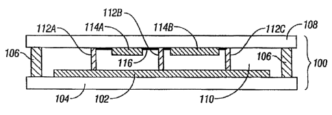
Figure 8 illustrates an embodiment of a package structure 100 in which a
backplate 108
serves as support for a variety of electronic components. As shown in the
figure, an array 102 of
interferometric modulators is located on a transparent substrate 104. The
array 102 thus provides
a means for modulating light and reflecting it through the substrate 104
towards a viewer, and the
substrate 104 provides a means for supporting the array 102. Sealant 106 joins
transparent
substrate 104 to the backplate 108, forming a protective cavity 110 around the
array 102. In this
embodiment, posts 112, which are located within the array 102 of
interferometric modulators,
provide additional support for the backplate 108, preventing the backplate
from coming into
contact with the array 102. The backplate 108 provides physical support for
various electronic
components 114A,B, discussed in greater detail below, which are located on the
underside of the
backplate 108.
In certain embodiments in which certain of the posts 112A-C are conductive, an
electrical
connection between the electronic components 114A,B and the array 102 can be
made by
bringing the conductive posts 112A-C into contact with conductive traces 116
located on the
backplate 108, which are in electrical connection with the components 114A,B.
Thus, such
conductive posts and traces provide a means for placing the electronic
components 114A,B in
electrical communication with the array 102.
In alternate embodiments in which the backplate provides physical support for
electronic
components, an electrical connection between the electronic components and the
array can be
made, in one example, by bringing conductive bumps located on the substrate
into contact with
conductive bumps located on the backplate. As another example, an electrical
connection
between the backplate and the interferometric array can be made by bringing
conductive posts
into contact with conductive bumps located on the backplate. A layer of
anisotropic conducting
film (ACF) or other conducting material can be employed in making these
electrical connections,
or these connections may be metal-to-metal connections, e.g. between two
conductive bumps.
Such alternate embodiments also provide means for placing the electronic
components in
electrical communication with the array.
In further embodiments, a flex cable or similar connector may be used to
provide an
electrical connection between a surface of the backplate and a surface of the
interferometric
modulator. It will also be understood that the electronic components need not
be located on the
underside of the backplate, as depicted in the embodiment of Figure 8. Some or
all of the
electronic components may be located on the upper surface of the backplate and
an electrical
connection may be made through the backplate using vias or electrical
feedthroughs.
Figure 9 shows a view of the underside of a backplate 120 onto which various
electronic
components have been fabricated. Row driver circuit 122 and column driver
circuit 124 are
located on the backplate 120, and electrical connections to and between the
driver circuits 122,
-11-
CA 02518396 2005-09-08
124 are provided through conductive traces 126. The driver circuits 122, 124
are in electrical
connection with a voltage generator 127 via traces 126. The driver circuits
122, 124 are also in
electrical communication with pads 132a and 132b, containing conductive bumps
134. A
graphical processing unit (GPU) 128 is in electrical connection with the
driver circuits 122, 124
via traces 126. In addition, low power circuitry 130 is in electrical
connection with GPU 128.
Pads 132a, 132b are configured to align with corresponding pads located on the
upper
surface of a transparent substrate, onto which an array of interferometric
modulators is provided.
The corresponding pads on the transparent substrate have conductive bumps, and
are in electrical
connection with the columns and the rows, respectively, of the array of
interferometric
modulators on the transparent substrate. Thus, bump-to-bump connections of the
type discussed
previously provide an electrical connection between the outputs of the driver
circuits 122, 124
and the rows and columns of the array. As discussed previously, one row of the
array at a time
may be addressed at a time by using the column driver circuit 124 to provide
information to each
column, and strobing the row to be addressed via the row driver circuit 122.
Thus, the electronic
components such as the driver circuitry provide a means for controlling the
state of the array of
interferometric elements, and the backplate 120 provides a means for
supporting the electronic
circuitry.
The voltage generator can be, for example, a commercially available unit, such
as the
Maxim MAX1605, MAX686, MAX1955 or MAX1561, or any circuitry which is capable
of
performing the desired voltage adjustments. In alternate preferred
embodiments, the voltage
generator can be developed for the specific application for which it is being
used. The voltage
generator 127 is provided with two inputs, 136a, 136b. In the embodiment of
Figure 9, the first
input 136a is at a supply voltage (e.g. 3.3V), and the second input 134b is at
ground. The voltage
generator supplies modified voltages to the row and column drivers 122, 124
via conductive
traces 126, so that a potential difference greater or less than the supply
voltage can be applied
across a row or column. Thus, the voltage generator 127 can be step-up
circuitry (also referred to
as a boost circuit), or step-down circuitry.
The GPU 128 can be, for example, a commercially available unit, such as the
Chips and
Technology 69030. In alternate preferred embodiments, the GPU circuitry can be
developed for
the specific application for which it is being used. In the embodiment shown
in Figure 9, the
GPU 128 is configured to accept three inputs 138A, 138B, 138C (clock, data,
and control,
respectively), and convert the data into a format which is required by the
particular row and
driver circuits 122, 124 (e.g. TFT, STN or CSTN format). In the embodiment of
Figure 9, the
GPU provides three signals to the column driver 124 (clock, data, and
control), and only two
signals to the row driver 122 (clock and control).
-12-
CA 02518396 2005-09-08
The low power circuitry 130 is used to allow the display to go into a low
power mode,
which can maintain a displayed image with relatively little power input. This
can be done, for
example, by stopping the clock and data signals from the GPU 128 to the row
and column driver
circuitry 122, 124. The use of such a low power circuit 130 is particularly
advantageous with
respect to displays employing an array of interferometric modulators, because
as discussed
previously, once an individual modulator in an array is moved to either a
released state or an
actuated state, a significantly smaller bias voltage is su~cient to maintain
the modulator in that
position. Additionally, almost no power is dissipated during this process, as
discussed above.
It will be understood that the electrical components depicted in Figure 9 are
exemplary.
Other embodiments may include more or less electrical components, and multiple
functions may
be performed by a single component. In addition, while the components of
Figure 9 are all
depicted as being on the underside of the backplate such that they are located
within the
protective cavity formed by the sealant once the package is assembled, certain
of the components
may be located elsewhere, such as on the top of the backplate or on a ledge of
the transparent
substrate extending beyond the sealant, such that the components are outside
the protective
cavity.
Electrical connections between the exterior of the package and the interior of
the package
can be made in multiple ways. When the backplane is glass, for example, or a
layer of any other
prefabricated material, the electrical connections may comprise conductive
traces running along
the surface of the backplate, such that the traces pass under the seals. When
the backplate is
fabricated for use as a backplate the backplate may advantageously be
fabricated to include
electrical vial, or feedthroughs, which provide an electrical connection
between the upper and
lower surface of the backplate. Such vias may be provided through glass or
other prefabricated
backplate materials, as well, but the addition of such vias may be more
difficult, time-consuming,
or costly.
In further embodiments, the electronic circuitry can be formed by depositing
thin-film
layers on a substrate which serves as the backplate, creating an application-
specific integrated
circuit (ASIC). An example of such an ASIC 140 is shown in vertical cross-
section in Figure 10.
The ASIC 140 is formed by depositing layers on a thin-film deposition ASIC
carrier 142, which
may be, for example, a layer of glass. The carrier 142 may comprise a glass
layer which serves as
the backplate for a display package similar to those discussed above. Any
suitable material may
be used as an ASIC carrier 140.
Amorphous silicon is then deposited on the ASIC carrier 142. In the embodiment
of
Figure 10, a layer 144 of amorphous p-type silicon has been deposited on the
carrier 142, and n-
type amorphous silicon is implanted in regions 145a, 145b, alternately
referred to as wells. Such
wells 145a,b will become the drains or sources of given transistors. In the
ASIC 140, the well
-13-
CA 02518396 2005-09-08
145a serves as the source of a transistor and the well 145b serves as the
drain. The silicon may
be deposited, for example, via photolithography, or via any other appropriate
technique known to
those skilled in the art. The p-n junctions between the base material in layer
144 and the wells
145a,b can be formed using techniques such as rapid thermal annealing (RTA) or
through the use
of lasers. While a p-type transistor is depicted in Figure 10, it will be
understood that an n-type
transistor can be created by depositing n-type silicon in layer 144, and
implanting p-type silicon
in the wells 145a,b.
The layer 144 of doped silicon is then coated with an insulation layer 146,
which in the
ASIC 140 of Figure 10 is a layer of Si02, but any appropriate insulation layer
may be used. The
deposition can be made by means of, for example, chemical vapor deposition
(CVD), or any
other appropriate method. Electrically conducting material 150, which may be
for example Mo,
is deposited on top of the insulation layer 146 between the wells 145a,b,
forming the gate of a
transistor. An etch process may be used to deposit the electrically conducting
material 150. An
additional layer 148 of insulating material, which in this embodiment may be a
nitrate such as
silicon nitrate, is deposited above the electrically conducting material 150
and the insulating layer
146.
Conductive pathways through the insulating layers 148, 146 are etched,
exposing the gate
150 and implant regions 145a,b. Metal 152 is deposited, forming connections to
the gate 150, the
source 145a, and the drain 145b, thereby creating transistors. The deposition
of this metal layer
can be done through the use of a mask, in order to etch the metal 152 in the
proper locations to
form the desired connections. Above layer 152, an additional layer of metal
153 is formed,
which may comprise a series of parallel lines (not depicted). Typically, metal
layers used in
ASICs, such as layer 153, conduct in only one direction, due to their
construction as a series of
parallel lines. Connections between transistors are formed by photographically
depositing metal
in a desired pattern to form layer 153. Layer 153 thus forms logic functions
by connecting
transistors in a desired pattern.
Above layer 153, a metallic layer 154 is formed. As can be seen in the Figure
10, layer
154 comprises a series of parallel lines oriented orthogonal to the page, and
thus, perpendicular to
the parallel lines in layer 153. Layer 154 is used to provide power to the
ASIC 140. Above layer
154, another metal interconnect layer 155 is formed, which completes more
complicated logic
connections. Above interconnect layer 155, a ground layer 156 is formed. Each
of layers 154-
156 may comprise parallel lines, and may be patterned through
photolithographic deposition.
Interconnections between the metal layers may be provided through vial, which
may be formed
by, for example, drilling holes in the metal layers and depositing metal in
the holes. In addition,
although in one embodiment, the layers 153-156 comprise parallel lines, in
alternate
embodiments, these may be formed by depositing layers which are not made of
parallel lines.
-14-
CA 02518396 2005-09-08
Thus, by depositing or etching the metal layers, and by forming
interconnections between the
layers, the desired interconnections between transistors may be created.
Above layer 156, a top metal layer 157 serves as an external interconnect
layer, providing
connections between the logic gates and the inputs/outputs of the ASIC. In the
embodiment of
Figure 10, the top metal layer 157 is not constructed of a series of parallel
lines, and thus
conducts in multiple directions, enabling more complex interconnection.
Masking and
photolithographic techniques may be used to etch the top metal layer, as may
any appropriate
method known to one skilled in the art. In an embodiment in which ASIC 140
forms electronic
circuitry in a display package such as those previously discussed, the metal
external connect layer
148 provides a connection between the ASIC 140 and the array of
interferometric modulators
(not shown), using any of the methods discussed in this application, or any
other suitable method.
In various embodiments, the deposition carrier 144 need not comprise glass,
but may
rather comprise any material suitable for carrying deposited thin film
circuitry. As previously
discussed with respect to Figure 9, the deposition carrier 144 may comprise
any of a variety of
features which enable electrical connections to be made between the interior
of a display package
and the exterior of a display package. These features may include, but are not
limited to,
electrical feedthroughs or vias, and electrical interconnection within the
deposition carrier 144.
Fabrication of electronic circuitry may provide multiple advantages in the
manufacture of
interferometric-based display packages. The customization of the circuitry
which is made
possible via fabrication allows for efficient use of space. Unlike other
display devices such as
LCDs, interferometric modulator-based displays allow for the inclusion of
electronic circuitry
which is located directly above the pixel array and within the "sandwich"
formed by the substrate
and the backplate. By positioning as much of the required electronic circuitry
in that location,
rather than on a ledge of the substrate exterior to the protective cavity, the
footprint of the display
can be minimized. In addition, the connections between the driver circuitry
and the array of
interferometric modulators can be complex, requiring as much as one output and
connection for
every row and column in the array. By fabricating the driver circuitry, a
greater amount of
control over the placement of these outputs and the interconnections between
these outputs and
the array is available. In addition, deposition of driver circuitry or other
electronic circuitry may
enable the creation of display packages which are thinner and less expensive
tha n display
packages which comprise prefabricated electronic circuitry.
Figure 11 shows an embodiment of a package 160 in which a electronic circuitry
162,
such as driver circuitry, is fabricated via thin-film deposition on the
underside of a backplate 164.
Metallic bumps 166A-C are aligned with metallic spacers, or support posts,
168A-C to provide an
electrical connection between the electronic circuitry 162 and an array 170 of
interferometric
-15-
CA 02518396 2005-09-08
modulators located on a substrate 172. Thus, the bumps 166A-C and posts 168A-C
provide a
means for electrically connecting the circuitry 162 and the array 170.
Sealant 174, along with substrate 172 and backplate 164, form a protective
cavity 176
around the array 170. An electrical connection between the exterior of the
package and the
electronic circuitry 162 is made via conductive traces 178, which run along
the underside of the
backplate 164, and over the sealant 174. The number of conductive traces 178
required for
operation of the electronic array depends on the type of electronic circuitry
162 fabricated on the
underside of the backplate 164. When the electronic circuitry 162 comprises
driver circuitry, the
required number of traces 178 extending between the interior and the exterior
of the package 160
can be greatly reduced. Similarly, the fabrication of GPU circuitry, boost
circuitry, or low power
circuitry on the underside of the backplate may simplify the required
interconnection between the
interior and exterior of the package 160.
While the package 160 shown in Figure 11 includes fabricated electronic
circuitry 162, it
will be understood that in alternate embodiments the electronic circuitry may
comprise
microchips or other prefabricated circuitry integrated with the fabricated
electronic circuitry. For
instance, driver circuitry and boost circuitry may be fabricated on the
underside of the backplate,
and connected with a commercially available GPU and low power circuit.
Figures 12A and 12B depict the assembly of a package 180 by thermal
compression.
Figure 12A depicts a vertical cross-section of the package 180 prior to
thermal compression, and
Figure 12B depicts a vertical cross-section of the package 180 after thermal
compression.
With respect to Figure 12A, it can be seen that a backplate 182 has a varying
thickness,
such that a depression area 185 is surrounded by thicker foot portions 184.
Electronic circuitry
186 is deposited within the depression area 185 and is in electrical
communication with the upper
surface of the backplate 182 through vial 206. The electronic circuitry 186 is
also in electrical
communication with conductive traces 188, which run along the underside of the
vias 206 and
extend at least to a lower surface 207 of the foot portion 184. A gold
conductive substance 190
and ACF layer 192 are positioned between the conductive traces 188 and a pad
194 located on
the upper surface of transparent substrate 196. It should be realized that the
pad 194 could also
be a trace, bump or other connector which provides electrical communication
with an array 200
of interferometric modulators. The pad 194 is in electrical communication via
conductive traces
198 with the array 200 of interferometric modulators located on the upper
surface of the
transparent substrate 196. Sealant 202 joins the backplate 182 to the
substrate 196, forming a
protective cavity 204 around the array 200.
Now with respect to Figure 12B, which depicts the package 180 in a more
compact form
after thermal compression, it can be seen that gold conductive substance 190
and ACF 192 are
compressed, providing an electrical connection between the electronic
circuitry 186 and the array
-16-
CA 02518396 2005-09-08
200, thereby enabling the electronic circuitry 186 to control the state of the
reflective elements in
the array 200. Thus, means for placing the circuitry 186 in communication with
the array 200 are
provided. It can be seen that the depression area 185 of the backplate 182 in
which the electronic
circuitry 184 was fabricated provides the electronic circuitry with clearance,
protecting the
circuitry from damage during the thermal compression process.
Figures 13A and 13B are system block diagrams illustrating an embodiment of a
display
device 2040. The display device 2040 can be, for example, a cellular or mobile
telephone.
However, the same components of display device 2040 or slight variations
thereof are also
illustrative of various types of display devices such as televisions and
portable media players.
The display device 2040 includes a housing 2041, a display 2030, an antenna
2043, a
speaker 2045, an input device 2048, and a microphone 2046. The housing 2041 is
generally
formed from any of a variety of manufacturing processes as are well known to
those of skill in
the art, including injection molding, and vacuum forming. In addition, the
housing 2041 may be
made from any of a variety of materials, including but not limited to plastic,
metal, glass, rubber,
and ceramic, or a combination thereof. In one embodiment the housing 2041
includes removable
portions (not shown) that may be interchanged with other removable portions of
different color,
or containing different logos, pictures, or symbols.
The display 2030 of exemplary display device 2040 may be any of a variety of
displays,
including a bi-stable display, as described herein. In other embodiments, the
display 2030
includes a flat-panel display, such as plasma, EL, OLED, STN LCD, or TFT LCD
as described
above, or a non-flat-panel display, such as a CRT or other tube device, as is
well known to those
of skill in the art. However, for purposes of describing the present
embodiment, the display 2030
includes an interferometric modulator display, as described herein.
The components of one embodiment of exemplary display device 2040 are
schematically
illustrated in Figure 13B. The illustrated exemplary display device 2040
includes a housing 2041
and can include additional components at least partially enclosed therein. For
example, in one
embodiment, the exemplary display device 2040 includes a network interface
2027 that includes
an antenna 2043 which is coupled to a transceiver 2047. The transceiver 2047
is connected to the
processor 2021, which is connected to conditioning hardware 2052. The
conditioning hardware
2052 may be configured to condition a signal (e.g. filter a signal). The
conditioning hardware
2052 is connected to a speaker 2045 and a microphone 2046. The processor 2021
is also
connected to an input device 2048 and a driver controller 2029. The driver
controller 2029 is
coupled to a frame buffer 2028 and to the array driver 2022, which in turn is
coupled to a display
array 2030. A power supply 2050 provides power to all components as required
by the particular
exemplary display device 2040 design.
-17-
CA 02518396 2005-09-08
The network interface 2027 includes the antenna 2043 and the transceiver 2047
so that
the exemplary display device 2040 can communicate with one or more devices
over a network.
In one embodiment the network interface 2027 may also have some processing
capabilities to
relieve requirements of the processor 2021. The antenna 2043 is any antenna
known to those of
skill in the art for transmitting and receiving signals. In one embodiment,
the antenna transmits
and receives RF signals according to the IEEE 802.11 standard, including IEEE
802.11(a), (b), or
(g). In another embodiment, the antenna transmits and receives RF signals
according to the
BLUETOOTH standard. In the case of a cellular telephone, the antenna is
designed to receive
CDMA, GSM, AMPS or other known signals that are used to communicate within a
wireless cell
phone network. The transceiver 2047 pre-processes the signals received from
the antenna 2043
so that they may be received by and further manipulated by the processor 2021.
The transceiver
2047 also processes signals received from the processor 2021 so that they may
be transmitted
from the exemplary display device 2040 via the antenna 2043.
In an alternative embodiment, the transceiver 2047 can be replaced by a
receiver. In yet
another alternative embodiment, network interface 2027 can be replaced by an
image source,
which can store or generate image data to be sent to the processor 2021. For
example, the image
source can be a digital video disc (DVD) or a hard-disc drive that contains
image data, or a
software module that generates image data.
Processor 2021 generally controls the overall operation of the exemplary
display device
2040. The processor 2021 receives data, such as compressed image data from the
network
interface 2027 or an image source, and processes the data into raw image data
or into a format
that is readily processed into raw image data. The processor 2021 then sends
the processed data
to the driver controller 2029 or to frame buffer 2028 for storage. Raw data
typically refers to the
information that identifies the image characteristics at each location within
an image. For
example, such image characteristics can include color, saturation, and gray-
scale level.
In one embodiment, the processor 2021 includes a microcontroller, CPU, or
logic unit to
control operation of the exemplary display device 2040. Conditioning hardware
2052 generally
includes amplifiers and filters for transmitting signals to the speaker 2045,
and for receiving
signals from the microphone 2046. Conditioning hardware 2052 may be discrete
components
within the exemplary display device 2040, or may be incorporated within the
processor 2021 or
other components.
The driver controller 2029 takes the raw image data generated by the processor
2021
either directly from the processor 2021 or from the frame buffer 2028 and
reformats the raw
image data appropriately for high speed transmission to the array driver 2022.
Specifically, the
driver controller 2029 reformats the raw image data into a data flow having a
raster-like format,
such that it has a time order suitable for scanning across the display array
2030. Then the driver
-18-
CA 02518396 2005-09-08
controller 2029 sends the formatted information to the array driver 2022.
Although a driver
controller 2029, such as a LCD controller, is often associated with the system
processor 2021 as a
stand-alone Integrated Circuit (IC), such controllers may be implemented in
many ways. They
may be embedded in the processor 2021 as hardware, embedded in the processor
2021 as
software, or fully integrated in hardware with the array driver 2022.
Typically, the array driver 2022 receives the formatted information from the
driver
controller 2029 and reformats the video data into a parallel set of waveforms
that are applied
many times per second to the hundreds and sometimes thousands of leads coming
from the
display's x-y matrix of pixels.
In one embodiment, the driver controller 2029, array driver 2022, and display
array 2030
are appropriate for any of the types of displays described herein. For
example, in one
embodiment, driver controller 2029 is a conventional display controller or a
bi-stable display
controller (e.g., an interferometric modulator controller). In another
embodiment, array driver
2022 is a conventional driver or a bi-stable display driver (e.g., an
interferometric modulator
display). In one embodiment, a driver controller 2029 is integrated with the
array driver 2022.
Such an embodiment is common in highly integrated systems such as cellular
phones, watches,
and other small area displays. In yet another embodiment, display array 2030
is a typical display
array or a bi-stable display array (e.g., a display including an array of
interferometric
modulators).
The input device 2048 allows a user to control the operation of the exemplary
display
device 2040. In one embodiment, input device 2048 includes a keypad, such as a
QWERTY
keyboard or a telephone keypad, a button, a switch, a touch-sensitive screen,
a pressure- or heat-
sensitive membrane. In one embodiment, the microphone 2046 is an input device
for the
exemplary display device 2040. When the microphone 2046 is used to input data
to the device,
voice commands may be provided by a user for controlling operations of the
exemplary display
device 2040.
Power supply 2050 can include a variety of energy storage devices as are well
known in
the art. For example, in one embodiment, power supply 2050 is a rechargeable
battery, such as a
nickel-cadmium battery or a lithium ion battery. In another embodiment, power
supply 2050 is a
renewable energy source, a capacitor, or a solar cell, including a plastic
solar cell, and solar-cell
paint. In another embodiment, power supply 2050 is configured to receive power
from a wall
outl et.
In some implementations control programmability resides, as described above,
in a driver
controller which can be located in several places in the electronic display
system. In some cases
control programmability resides in the array driver 2022. Those of skill in
the art will recognize
-19-
CA 02518396 2005-09-08
that the above-described optimization may be implemented in any number of
hardware and/or
software components and in various configurations.
While the above detailed description has shown, described, and pointed out
novel
features of the invention as applied to various embodiments, it will be
understood that various
omissions, substitutions, and changes in the form and details of the device or
process illustrated
may be made by those skilled in the art without departing from the spirit of
the invention. As will
be recognized, the present invention may be embodied within a form that does
not provide all of
the features and benefits set forth herein, as some features may be used or
practiced separately
from others.
-20-