Note: Descriptions are shown in the official language in which they were submitted.
CA 02518476 2005-09-07
WO 2004/084460 PCT/US2004/007496
[0001] ENHANCED AUTOMATIC GAIN CONTROL MECHANISM
FOR TIMESLOTTED DATA TRANSMISSIONS
[000] FIELD OF IhT~I~TTIO1~T
[000] The present invention generally relates to wireless communication
systems. Fore particularly, the present invention relates to an automatic gain
control (AGC) circuit for a timeslotted communication system, such as a time
division duplex (TDD), time division nnultiple access (TDl~) or time division-
code division multiple access (TD-CDl~lA) system.
[0004] BACKGROUND
[0005] In a conventional wireless communication system, the baseband
signal at the receiver is converted from an analog format into a digital
format so
that the useful information in the signal can be recovered via a sequence of
digital processes. Typically, an analog-to-digital converter (ADC) is used to
achieve this conversion. In general, the more output bits the ADC has, the
larger
the dynamic range of the input signal the ADC can support. However, this
results in a more expensive ADC, as well as higher costs for some of the other
receiver components. Given the number of output bits, if the power of the
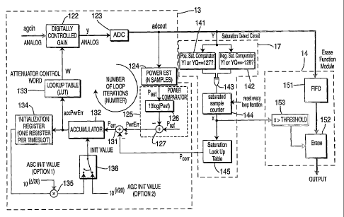
input
signal is too large, the output of the ADC may be saturated. On the other
hand,
if the power of the input signal is too small, the output of the ADC may be
severely quantized. For both of these scenarios, the information expected to
be
recover ed at the receiver may be degraded or lost.
[0006] A common approach for solving this problem is to apply a
dynamically adjustable gain amplifier in front of the ADC so that the input
signal of the ADC can be maintained within desired limits. Typically, the
adjustable gain is controlled using an AGC circuit.
[0007] It is well known in the art that power varies significantly between
adjacent timeslots in a TDD frame and between the same time slot in adjacent
frames due to variable data rates or a variable nmnber of active users in a
-1-
CA 02518476 2005-09-07
WO 2004/084460 PCT/US2004/007496
timeslot. In order to determine the correct gain level for a given timeslot,
the
AGC estimates the symbol power of the first N symbols in the timeslot as they
are received. During this estimation process, the symbols may be lost for data
estimation due to ianperfect gain control during this time. Also, depending on
the
ax~itial accurac~% o~the gaix~a estixaatr~, this estan~aation
procedu~°e n~aay t~Le a long
time; accuracy in this case is the difference between the gain applied at the
start
of the timeslot and the final "correct99 gain as determined by the AGC
circuit.
[0003] A typical TDD fraxx~e generally comprises fifteen timeslots. Each of
tlae timeslots includes two data bursts that are separated by a midamble,
followed by a guard period at the end of the timeslot. The data bur sts
transx~nit
the desired data, and the midamble is used to perform. channel estimation.
[0009] It would be desirable to have a system and method which avoids the
accuracy and data loss problems of current AGC methods.
[0010] SUMMARY
[0011] According to the present invention, the initial gain applied by a
digital AGC circuit in a timeslot is determined using a final calculated gain
from
the same timeslot in the previous frame together with an offset factor. An
erase
function is activated for a given data sample block when the number of
saturated
data samples that are detected within the block exceeds a threshold value. The
power measurement made by the AGC circuit and used to update the gain is
adjusted based on the number of measured data samples that are saturated.
These elements provide a gain limiting function and allows limiting of the
dynamic range for further signal processing.
[0012] BRIEF DESCRIPTION OF THE DRAWINGS
[0013] Figure 1 is a general block diagram of an automatic gain control
(AGC) circuit made in accordance with the present invention;
[0014] Figure 2 is a block diagram of an AGC circuit constructed in
accordance with the present invention;
-2-
CA 02518476 2005-09-07
WO 2004/084460 PCT/US2004/007496
[0015] Figure 3is a flow diagram showing the AGC calculation performed
in accordance with one embodiment of the present invention; and
[0016] Figure 4 is a timing diagram of the sequence of events within a
timeslot.
[0017] DETAILFD DESCl~IPTI~N ~F TI-IE PREFFRRFD ElllB~DI1~ENT(S)
[001] The present invention will be described with reference to the
drawing fngures wherein like numerals represent like elements throughout.
[00191 The present inventi~n is useful in wireless communications, such as
in conjunction with a third generation partnership program (3GPP) system
utilising the time division duplex mode. It is noted, however, that the
present
invention is applicable to any wireless communication system. Such systems use
base stations (BS) and wireless transmitlreceive units (WTRUs). A WTRU
includes, but is not limited to a user equipment, mobile station, fixed or
mobile
subscriber unit, pager, or any other type of device capable of operating in a
wireless environment. A base station includes, but is not limited to, a Node
B,
site controller, access point or other interfacing device in a wireless
environment.
While CDMA under the 3GPP protocol is described in connection with exemplary
embodiments, the invention has general applicability to other wireless or
wired,
and timeslotted or non-timeslotted communication systems.
[0020] In accordance with the present invention, the following assumptions
are made. First, the cell search process has been completed successfully and
the
timeslot timing has been acquired. Second, the cell search AGC provides the
initial value of gain to be used for the first time slot, (i.e., the Broadcast
Channel
(BCH) timeslot) that is demodulated after cell search has successfully
completed.
Third, the total gain of the RF chain has been applied to the received signal
and
is reflected in the values of the signal at the input of the digital
controlled gain
block.
[0021] The AGC process in accordance with the present invention is
timesl~t-based. Referring to Figure 4, a timing diagram is shown. For each
timeslot 200, there is a start of the timeslot 203, and a plurality of
sampling
-3-
CA 02518476 2005-09-07
WO 2004/084460 PCT/US2004/007496
periods NS~P 211-213, separated by a plurality of skip periods NSF 221, 222.
The
end of the data burst 231 is followed by a guard period 232, which is adjacent
to
the end 233 of the timeslot 200. Generally, for each timeslot 200, the
digitally
controlled gain is initialized, followed by a plurality of adjustments so that
the
power at the output of AI~C becomes close to a reference povSer level.
[0022] A block diagram of the AGC unit 11 made in accordance with the
present invention is shown in Figure 1. The AGC unit 11 includes an AGC loop
13, an erase function module 14, and a saturation detection circuit 17. An
input
signal is received by the ~9GC loop 13, which processes the input signs.l and
outputs to the erase function module 14 and the saturation detection circuit
17.
The saturation detection circuit 1'7, receives the output from the AGC loop 13
and
provides its output to both the AGC loop 13 and to the erase function module
14.
The erase function module 14 in turn provides its output to subsequent
receiver
processes.
[0023] In operation, the AGC loop 13 samples an input signal and processes
the signal to provide an output to the saturation detection circuit 17 and to
the
erase function module 14. The AGC loop 13 determines the proper AGC level,
utilizing an input from the saturation detection circuit 17. The saturation
detection circuit 17 provides a count of the number of samples within a sample
block (NS~P) that are saturated. If the number of saturated samples within the
sample block (NSF,) exceeds a predetermined threshold, the erase function
module 14 replaces all of the samples within an extended block (NSF + NSHIP)
with zeros. The saturation count is also used by AGC circuit 11 to compensate
for the overestimation of the required gain, due to the presence of saturated
samples.
[0024] The output for the AGC circuit 11 comprises digital data samples
from the I and ~ channels for subsequent receiver processes.
[0025] The frequency of operation of the AGC circuit 11 is determined by a
need to effect processing for the signals which are received in each timeslot.
_4_
CA 02518476 2005-09-07
WO 2004/084460 PCT/US2004/007496
Therefore the frequency of operation is such that the AGC operates on each
active
received timeslot.
[0026] Referring now to Figure 2, there is shown a detailed block diagram
of a cir cuit 100 for executing the enhanced AGC process of the present
invention.
The circuit 100 includes the AGC loop 13, the er ase function n~ociule 14,
a~a.d the
satur anon detection module 17.
[002°7] The AGC Loop 13 includes a digitally controlled gain circuit
122, an
ADC 123, a power estimator 124, a power comparator 125, a summer 131, an
accumulator 132, a control word look-u.p table (IdUT) 133, an initialization
register 134, a multiplier 135, and an initial value selector 136.
[002] The digitally contgolled gain circuit 122 receives an input analog
signal (agcin) and processes the analog signal to provide a gain-controlled
analog
input (y) to the ADC 123. The ADC provides a digital sample output
(adcSampout). The digital sample output (adcSampout) is provided to the
saturation detection circuit 17, the erase function module 14 and the power
estimation circuit 124.
[0029] The power estimation circuit 124 estimates the power of the digital
sample output (adcSampout) and provides this estimate to the power comparator
125.
[0030] The power comparator 125 preferably includes a log estimator 126.
Using a log function linearizes the AGC loop in dB, providing loop response
faster
than what would be achieved without the log function. The power estimate Pest
of
the log estimator 126 is input to a summer 127 which compares the power
estimate Pest of the log estimator 126 with a power reference (Pref). The
output
from summer 127 is an error signal (pwrErr) that indicates the power setting
error. This is calculated as follows:
wr~Err =10 ~ to
Pesr
Equation (1)
[0031] The power setting error pwrEr-r output from the summer 127 is
input into a second summer 131, which adjusts the power setting error pwr~Err
by
_5_
CA 02518476 2005-09-07
WO 2004/084460 PCT/US2004/007496
a correction factor p~~m . As will be explained in detail hereinafter with
reference
to the saturation detection circuit 17, the correction factor p~~~ depends on
the
saturation count.
[0032] The summer 131 uses the following inputs to calculate a power errcar
sagnal Perr' 1) the power setting error ~aivr~r~r from the p~wer comparator
circuit
125; and 2) a power correction value Pco~. fr om a satur ation LUT 145. The
output
of the summer 131 is a power error signal Pe~. which includes saturation level
adjustment. It is calculated as follows:
err - ~W ~~'°j~f' - ~carr
Equation (2)
[0033] The pure~se of the power error signal Perr is to compensate for the
over estimation of the gain due to underestimating the received power because
of
saturations. The power error signal Pe~. is then input to the accumulator 132.
[0034] The accumulator 132 accumulates the power error signal Pe,.r and
provides its output accPwrErr to the control word LUT 133 and to the
initialization register 124.
[0035] The control word LUT 133 provides a gain control word (W) to the
digitally controlled gain circuit 122 that corresponds to the desired gain
setting
determined in the current iteration. In one preferred embodiment, the gain
setting is in steps of 1 dB for a total range of 0 to 75 dB, although this is
just one
example of such a setting. The input of the LUT 133 is the accumulated error
signal accPwrErr from the accumulator 132. The output of the LUT 133 is the
gain control word (W) which adjusts the digitally controlled gain circuit 122
to
achieve the desired gain setting.
[0036] The output accPwrErr of the accumulator 132 is also provided to the
initialization register 134. The operation of the AGC loop 13 requires storage
of
the accumulator 132 values at the end of each timeslot. These values are
stored
in the initialization register 134. There is one initialization register 134
for each
timeslot. The output of the initialization register 134 is multiplied by a
factor of
10~° using multiplier 135, (where ~ is a pre-prograxumed ~ffset
factor), to provide
-6-
CA 02518476 2005-09-07
WO 2004/084460 PCT/US2004/007496
a first input (option 1) to the initial value selector 136. The first input is
a
preferred embodiment of the present invention whereby the accumulator value of
a timeslot in the previous frame stored in the initialization register 134 is
used
along with the offset factor ~ , to calculate the initial gain applied in the
curs ent
tixxaeslot. An e~ax~aple range for the offset f~.ctor ~ is fr~m 0 to -20 dB in
1 dB
steps.
[0037] A second input (option 2) to the initial value selector 136 is a
predetermined value. An example range for this value is from 0 to -75 dB in 1
dB steps.
[0033] The switching circuit 136 selects between the f rst and second inputs
to provide an initialization value to the accumulator 132. The selection of an
initial value via the selector 136 is accomplished with a gain initialization
indication. If gain initialization option 1 is indicated, the initial gain is
the final
calculated gain from the previous frame for the current timeslot adjusted by
the
offset factor 0. If gain initialization option 2 is indicated, the initial
gain is a
predetermined fixed value, t, is applied to the accumulator as 10 'ZO . An
example
range for i is 0 to -75 dB, although the specific value is dependent upon the
implementation. After initialization, the accumulator 132 receives inputs,
once
per iteration, from the power comparator 125.
[0039] The signal from the ADC 123 (adcSampout) is also provided to the
saturation detection circuit 17. The saturation detection circuit 17
compensates
for under-valued power estimates due to saturated samples. The saturation
detection circuit 17 includes a positive saturation comparator 141, a negative
saturation comparator 142, an OR-gate 143, a saturated sample counter 144 and
a saturation LUT 145. The saturated sample counter 144 provides outputs to
both the saturation LUT 145 and to the erase function module 14.
[0040] The positive and negative saturation comparators 141, 142 detect
saturated samples. In the comparators 141, 142, if both I and ~,1 samples are
saturated at the same time, it counts as a single saturated sample, not two
saturated samples. The effect ~f OR-gate 143 is that either a negative ~r
positive
_7_
CA 02518476 2005-09-07
WO 2004/084460 PCT/US2004/007496
saturation counts as saturation. The saturated sample counter 144 counts the
number of saturated samples in a given sample block (NS~P).
[0041] The saturation LUT 145 maps the number of saturated samples to
power adjustment in order to compensate ~or the overestimati~n of gain due to
the saturated samples. It should be noted that the reason that the Q~.ig~ is
overestimated when there are saturated samples is that the saturated samples
are clipped or reduced versions of what the true value would be if there were
more ADC bits and the signal was not clipped.
[004] The saturation detection circuit 17 provides protection to
subsequent receiver processes for extreme cases of signal saturation, by
trigger ing the er asing of samples. The saturation detection circuit 17
triggers
the condition under which the erase function module 14 is activated for a
given
sample block (NSF + NSHIP). The condition is satisfied when the saturation
count
exceeds a predetermined threshold. Each given sample block (Ns~P + NSHIP) is
handled separately. As the loop iterates, the probability of saturation drops
considerably. Thus, as a practical matter, it is unlikely that any sample
block
(NSF + NSHIP) other than possibly the first one in the timeslot will trigger
the
erase function module 14.
[0043] Although the AGC design described hereinafter in one embodiment
of the invention uses fixed-point settings derived from the basic assumption
that
the ADC word size is 3 bits (7 magnitude; 1 sign bit), it should be noted that
the
ADC word size is given by way of example and thus this particular ADC word
size is not required.
[0044] In an exemplary embodiment, the saturation LUT 145 is required to
provide a six-bit output as a function of the saturation counter 144. The LUT
145
has length equal to NsaMP. It has an input (x) from the saturation sample
counter 144 and an output of F~o~., the power error correction value.
[0045] In operation, the saturation detection circuit 17 receives the output
from the ADC 123. saturation detection is started by counting the number of
samples output (adcSampout) from the signed 3-bit ADC that have values -123 or
_$_
CA 02518476 2005-09-07
WO 2004/084460 PCT/US2004/007496
+127. The count is performed for every sample block NsAMP and it is reset for
each iteration of the sample block (NS~P + NSHIP). The number of saturated
samples (x) in a sampling block Ns~ is used to form the estimate of the amount
of satur ation. If either the I or ~ parts of a given input vela a is -123 or
+127, the
satuxstion counter 143 is ia~crexga.ex~ted. The resulting count apt the ena~
of a
sampling block Ns, which is a count of the nmxgber of saturated samples (~)
that occurred within the sampling block Ns, is then output to the saturation
LUT 145 and the erase function module 14.
[0046] Based on the number of saturated samples (~~) during a sampling
block I~Ts, the power error correction value P~o~. is output from the
saturation
LUT 145. This value is an estimate of, and is pr oportional to, the amount of
saturation that has occurred.
[0047] As described hereinbefore, this value is subtracted from the output
of the power comparator block 125. The power error correction value P~o~. is
based on the same sampling block (NSAMP) as the power estimate Pest, making
the
pair fully synchronized. Because the power estimates are preferably in
logarithmic form, they allow for a smaller word size of the contents of the
saturation LUT 145.
[004] The output of the ADC 123 is also provided to the erase function
module 14. The erase function module 14 includes a FIFO 151, an erase circuit
152 and a compare circuit 153.
[0049] The erase function module 14 makes the decision to erase data
samples, (i.e., I and ~ samples are set to zero), based on the number of
saturated
samples (x) from the saturation detection circuit 17. When the number of
saturated samples (x) exceeds a predetermined threshold, all of the samples in
the corresponding period (NS~P + NSHIP) for a given loop iteration are erased.
[0050] FIF~ 151 must be appropriately sized, since the sampling block
NSF must be received before a decision can be made, and the number of
saturated samples (x) is being counted during the sampling block NSA~.
-9-
CA 02518476 2005-09-07
WO 2004/084460 PCT/US2004/007496
[0051] The output from the erase function module 14 is the received data
with some of the samples set to zero (erased).
[0052] Figure 3 is a flow diagram of a method 300 of AGC calculation
performed in accordance with one embodiment of the present invention. In the
guard peraocl_ of the previous tixxaeslot, the g~.in is set (step 302). It is
voted that
the gain xnay be set Casing option 1 or optiox~ 2. In option 1, the gain is
the value
stor ed in the register f~r the timeslot adjusted by the offset. In eption 2,
the gain
is a fired value. The selection of option 1 versus option 2 is pre-determined.
I~,egardless of choosing option 1 ox option. 2, the initial AGC gain value is
set
before the start of the timeslot.
[0053] At the start of an iteration, an AGC power calculate~n begins
(step 304). The start of an iteration is either at the beginning of a timeslot
or
immediately after the previous iteration in the timeslot. Saturation detection
is
run (step 306). This is followed by computing Pest, P~oL,., Per, and applying
these
values to the accumulator and the decision whether to erase the data symbols
in
the iteration is made (step 308). An updated AGC gain value is provided to the
radio controller (step 310), and the value is stored in the register for the
timeslot
wherein the iteration began (step 312). A skip period begins (step 314) and
then
ends (step 316). This is repeated (steps 304-316) for N iterations or until
the end
of the timeslot (step 318).
-10-