Note: Descriptions are shown in the official language in which they were submitted.
CA 02518625 2005-09-09
PCT/AU2004/000283
PvOPER~AABUeGmum Iamb process spec' ul7edx~I3lO5I~5 Received I 3 May 2005
A LAMP AND A PROCESS FOR PRODUCIl~'G A LAMP
FIELD OF THE INVENTION
The present invention relates to a process for producing a lamp assembly, a
process for
producing a lamp, and an array of light source assemblies.
The present invention is an improvement on the subject matter of International
Patent No.
PCT/AU03/00724, the entire subject matter of which is incorporated herein by
reference.
BACKGROUND TO THE INVENTION
Solid-state light sources, such as light emitting diodes (LEDs), are often
proposed as the
light sources of the future for both specialist and general lighting
applications. Recent
improvements in the efficiency and the colours and intensity of illumination
produced by
such devices has led to their increasing adoption for many lighting
applications. Even
though LEDs are not yet as efficient as fluorescent light sources, their
extremely long
lifetime has led to their widespread use in non-domestic lighting
applications.
In order to obtain a sufficient intensity of light for many applications,
lamps have been
developed that include many individual LEDs grouped together to provide a high
intensity
light beam that has the appearance of being produced by a single light source.
Because the
divergence of the light beam produced by each individual LED is relatively
small, the
LEDs can be arranged in slightly different orientations (e.g., on a non-planar
surface) to
provide a composite light beam having a relatively large angular divergence
suitable for
general lighting applications, as described in International Patent No.
PCT/AU03/00724.
Unfortunately, existing processes for producing such lamps are time consuming,
difficult,
and consequently expensive. In. particular, the making of electrical
connections to the
individual light sources in such lamps can involve non-standard assembly
processes that
can be quite cumbersome. Far example, electrical connections to LEDs have -
previously
Amended Sheet
CA 02518625 2005-09-09
PCT/AU2004/000283
P'.vOPERUtABUadnwen Iamb V« ~<-crt7s dac-13rO5~O5 Received 13 May 2005
-2-
been made using wire bonding machines. However, this can be difficult when
these
connections are to be made between connection points that are not in the same
horizontal
plane, such as when the LEDs are mounted on a non-planar surface, because wire
bonding
machines are not readily suited to making such connections.
A further difficulty of existing lamps incorporating solid-state light sources
is the heat
generated by these devices, which in the case of standard LEDs is of the order
of one Watt
per square millimetre. Standard LEDs typically produce about 100 milliWatts of
heat,
which, when the LEDs are packaged individually, is quite manageable. Even in
densely
packed arrays with many such LEDs, the heat dissipation issue can be
successfully
addressed. However, larger LEDs with areas exceeding one square millimetre are
now
becoming commonplace, and each of these LEDs can generate more than one Watt
of heat.
Because this heat is generated in a small physical volume, and the surface
area of each
LED is small, the temperature of each LED can rise dramatically unless this
heat can be
I S effectively dissipated. In general, LEDs operate less efficiently as the
temperature of the
active region increases. There is also a strong body of evidence to suggest
that LEDs are
degraded by extended operation at high temperatures.
It is desired to provide a process for producing a lamp assembly, a process
for producing a
lamp, and an array of light source assemblies that alleviate one or more
difficulties of the
prior art, or at least that provide a useful alternative.
SUMMARY OF THE INVENTION
In accordance with the present invention, there is provided a process for
producing a lamp
assembly having a plurality of light emitting semiconductor devices mounted to
a non-
planar support, the process including:
forming a plurality of substantially rigid non-planar electrical connectors,
each of
said connectors including an electrically conductive annular portion and a
plurality of
contacts projecting from and electrically connected to the annular portion;
and
Amended Sheet
roc~i~ri
CA 02518625 2005-09-09
PCT/AU2004/000283
P.vOPERUtABUdmum Iamb D«' ~~ - ~a-da~ U~05I05
Received 13 May 2005
-3-
mounting the plurality of contacts of said non-planar electrical connectors to
respective
electrically conductive locations of said lamp assembly to provide at least
one path for
conducting electrical current through said plurality of light emitting
semiconductor
devices.
The present invention also provides a process for producing a lamp, including:
forming an electrically conductive receptacle having a substantially planar
base and
a substantially planar peripheral region;
forming a substantially planar electrical insulator on said substantially
planar
peripheral region;
forming a substantially planar electrically conductive contact on said
substantially
planar electrical insulator;
mounting a light source on said base of said receptacle;
making a first electrical connection between said substantially planar
electrically
conductive contact and a first contact of said light source, and a second
electrical
connection between said electrically conductive receptacle and a second
contact of
said light source; and
encapsulating said light source and said electrical connections to provide a
light
source assembly for mounting on an electrically conductive support, wherein an
unencapsulated portion of said substantially planar electrically conductive
contact
provides a first electrical contact to said light source mounted in said
receptacle, and
the electrically conductive receptacle provides a second electrical contact to
the light
source.
2~ The present invention also provides a process for producing a lamp,
including:
forming an array of electrically conductive receptacles interconnected by
receptacle
joining portions, each of said receptacles having a substantially planar base
and a
substantially planar peripheral region;
forming an array of substantially planar electrical insulators on said
peripheral
regions of said receptacles;
Amended Sheet
1PEA/AU
CA 02518625 2005-09-09
PCT/AU2004/000283
P',~oE0.UiA8Uedmum lamp Proccu syec - an7a.doc~ l7NSi03
Received 13 May 2005
forming an array of substantially planar electrically conductive contacts on
said
electrical insulators;
mounting light sources on the bases of said array of receptacles;
making first electrical connections between a first contact of each light
source and
the electrically conductive contact of the corresponding receptacle, and
second
electrical connections between a second contact of each light source and the
corresponding receptacle; and
encapsulating said light sources and said electrical connections to form an
array of
light source assemblies, wherein an unencapsulated portion of the
substantially planar
electrically conductive contact of each receptacle provides a first electrical
contact to
the light source mounted in that receptacle, and the electrically conductive
receptacle
provides a second electrical contact to the light source.
The present invention also provides a light source assembly produced by any of
the above
processes.
The present invention also provides a lamp assembly produced by any of the
above
processes.
The present invention also provides a lamp produced by any of the above
processes.
The present invention also provides a lamp production system having components
for
executing the steps of any of the above processes.
The present invention also provides an array of light source assemblies,
including:
an array of electrically conductive receptacles for receiving respective light
sources,
said receptacles interconnected by receptacle joining portions, each of said
receptacles
having a substantially planar base and a substantially planar peripheral
region;
Amended Sheet
TPEA/AU
CA 02518625 2005-09-09
PCT/AU2004/000283
p woERU2A BUedmum ~am0 Rouss spec s"N sn SW nadmmu doo.l L1~9A
Received 12 October 2004
-4A-
an array of substantially planar electrical insulators on said peripheral
regions of
said electrically conductive receptacles;
an array of substantially planar electrically conductive contacts on said
electrical
insulators;
light sources mounted on the bases of said array of electrically conductive
receptacles;
first electrical connections between said electrically conductive contacts and
first
contacts of said light sources, and second electrical connections between said
electrically conductive receptacles and second contacts of said light sources;
and
said light sources and said electrical connections being encapsulated, wherein
an
unencapsulated portion of the substantially planar electrically conductive
contact of each
receptacle provides a first electrical contact to the light source mounted in
that receptacle,
and the electrically conductive receptacle provides a second electrical
contact to the light
source.
BRIEF DESCRIPTION OF THE DRAWINGS
Preferred embodiments of the present invention are hereinafter described, by
way of
example only, with reference to the accompanying drawings, wherein:
Figures 1 to 3 are perspective, side, and plan views, respectively, of a lamp
assembly according to one preferred embodiment of the invention;
Figure 4 is a flow diagram of a lamp production process according to one
preferred
embodiment of the invention;
Figure 5 is a flow diagram of a cup assembly process forming pan of the lamp
production process of Figure 4;
Figure 6 is a plan view of an array of cups used in lamp assemblies of the
type
shown in Figures 1 to 3;
AMENDED S~tE~ s
CA 02518625 2005-09-09
WO 2004/082021 PCT/AU2004/000283
-5-
Figure 7 is a plan view of a single cup of the cup array;
Figure 8 shows a plan view and a cross-sectional side view of the cup
separated
from array;
Figure 9 is a plan view of an array of cup contact rings of the lamp assembly;
Figure 10 is a plan view of a single cup contact ring of the cup contact ring
an~ay;
Figure 11 shows a plan view and a cross-sectional side view of the cup contact
ring
separated from the cup contact ring array;
Figure 12 is a plan view of a cup assembly of the lamp assembly;
Figure 13 is a side cross-section view of the cup assembly;
Figure 14 is a plan view of a cup support lead frame of the lamp;
Figure 15 is a plan view of the cup support lead frame after its curved
portion has
been partitioned into three portions and three openings have been cut in each
portion, and
showing three cup assemblies mounted in the openings in a left hand portion;
Figure 16 is a plan view of an array of annular connector pairs of the lamp;
Figure 17 is a plan view of a single annular connector pair of the annular
connector
array;
Figures 18 and 19 are plan views of inner and outer annular connectors,
respectively, ~f the annular connector pair;
Figure 20 is a side view of the cup support lead frame encapsulated within an
optical package;
Figure 21 is a side view of the encapsulated cup support lead frame clamped
between cover and base components of an outer package;
Figures 22 shows plan and side views of the cover of the outer package;
Figure 23 shows plan and side views of the base of the outer package;
Figure 24 shows plan and side views of the encapsulated lamp assembly in the
outer package;
Figure 25 is a side view of the encapsulated and packaged lamp assembly after
lead
forming;
Figures 26 and 27 are plan and side views, respectively, of the packaged and
encapsulated cup support lead frame prior to removal of redundant portions of
the lead
frame sheet;
CA 02518625 2005-09-09
WO 2004/082021 PCT/AU2004/000283
-6-
Figure 28 is a side view of the lamp;
Figure 29 is a side view of an alternative embodiment of a lamp having an
alternative arrangement of contact leads;
Figures 30 and 31 show plan and cross-sectional side views, respectively, of
an
alternative cup assembly having a circular encapsulant;
Figures 32 to 34 are perspective, side, and plan views, respectively, of a
further
alternative lamp assembly;
Figures 35 is a plan view of yet a further alternative cup support lead frame
partitioned into twelve portions for supporting respective cup assemblies,
and, using an
alternative contact configuration; and
Figure 36 is a plan view of yet another further alternative and unpartitioned
cup
support lead frame supporting twelve cup assemblies, having a contact
configuration that
allows each cup assembly to be independently controlled.
DETAILED DESCRIPTION OF THE PREFERRED EMBODIMENTS
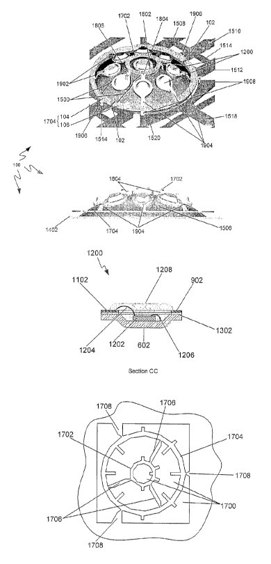
A lamp includes a lamp assembly 1009 as shown in Figures 1 to 3, including
nine light
source assemblies 1200 mounted on an electrically conductive light source
support 1406.
Each of the light source assemblies 1200 contains a light source, being a
light-emitting
diode (LED) that emits a beam of light from its surface when electric current
is passed
through the LED. Each LED is preferably of a type having a relatively large
active area
(e.g., in the range 0.5 - 1.5 mm2), requiring an operating current which can
be up to 3~0 -
400 mA; however, smaller area LEDs can alternatively be used.
The LEDs are mounted on the concave side of each light source assembly 1200
and are
therefore not visible in Figures 1 to 3. In the arrangement shown, the light
source
assemblies 1200 are mounted on the convex outer surface of the support 1406
with their
base part directed towards the concave inner side of the light source support
1406.
Consequently, the light beams generated by the LEDs point in different
directions,
providing uniform illumination over a relatively wide divergence angle
suitable for many
lighting applications.
CA 02518625 2005-09-09
WO 2004/082021 PCT/AU2004/000283
-7_
The lamp 100 is made by executing a lamp production process, as shown in
Figure 4. The
lamp production process is a batch process whereby many instances of the lamp
100 are
made simultaneously in an array form. The process begins by forming light
source
assemblies 1200, referred to hereinafter as cup assemblies 1200, using a cup
assembly
process 402, as shown in Figure 5. This process begins by forming an array 600
of cup or
bowl-shaped receptacles 602 referred to hereinafter as cups 602, as shown in
Figure 6. The
cup array 600 is manufactured from relatively thick (e.g., at least 0.3 mm)
sheet metal to
provide an electrically conductive cup that allows substantial heat flow
through the cup
602. However, it will be apparent that the cups 602 can alternatively be
manufactured from
any other material having substantial electrical and thermal conductivity and
mechanical
rigidity. The array 600 can be produced in continuous roll form from a sheet
of suitable
material, or alternately in discrete lengths, as illustrated.
As shown in Figure 7, each cup 602 is formed using a standard stamping
technique to
deform the sheet to create the cup depressions or cavities, and removing
portions 702 of
the sheet. The cup 602 remains connected to the sheet by joining portions 704.
As
described below, the cups 602 are separated from the array 600 in a later step
by cutting
the joining portions 704 along the path 706. For the purposes of illustration,
Figure 8
provides a plan view and a side-view cross-section of a separated cup 602. The
cup 602 is
generally shaped like a bowl or shallow cup having a recess defined by a flat
base 802 and
an outer rim 804 joined by sloping sides 806. The cup includes residual
portions 808 of the
joining portions 704, and a contact area or tab 810 projecting outwards from
the rim 804.
After the cup array 600 has been formed, an array 900 of contact loops or
rings 902 is
formed at step 504 by stamping, etching, laser cutting, or some other form of
machining, or
whichever method was used to form the cup array 600, except that the sheet
metal from
which the contact rings 902 are formed is thinner that that used in the cups
602 because the
contact rings 902 do not need to conduct heat. As shown in Figure 10, each
contact ring
902 is formed by removing portions 1002 from the sheet, leaving the contact
ring attached
to the array 900 by contact ring joining portions 1004. The contact rings 902
are separated
CA 02518625 2005-09-09
WO 2004/082021 PCT/AU2004/000283
_g_
from the array 900 in a later step by cutting the joining portions 1004 using
a cutting tool
to follow a cutting path 1006. The cutting tool also follows a second cutting
path 1008 to
remove a central portion from the contact ring 902 to define a circular loop
or ring
structure with a central hole 1010. Figure 11 shows a plan view and a side
view cross-
S section of the contact ring 902 after cutting. The contact ring 902 includes
an outwardly
projecting contact area or tab 1102 in the plane of the ring 902.
The outer dimensions of each contact ring 902 are the same as those of the rim
804 and
contact tab 810 of each cup 602. Although the cup rims 804 and contact loops
or rings 902
are shown having a generally keyhole-like shape comprising a circular annular
loop with a
sharply-defined outwardly proj ecting contact area 810,1102, other shapes can
be
alternatively used, although it is preferred that the cup rims and contact
loops have at least
the same outer shape so that they can be easily aligned relative to each
other. For example,
alternative embodiments can be devised in which the annular cup rims and
contact loops
are not circular in shape, but could alternatively be oval, square, or
rectangular annular
loops, for example. Furthermore, although it is preferred that the loops are
closed, it can be
envisaged that the loops could be open loops including a small gap.
At step 506, an array (not shown) of loop or ring-shaped insulators 1302
having the same
dimensions (with the possible exception of thickness) and orientation as the
contact rings
602 is formed from a sheet of electrically insulating material such as
Folyimide.
Alternatively, the sheet of insulation can be formed as an array of circular
holes having the
same diameter as the inner diameter of the contact rings 602. In either case,
excess
insulation is trimmed from the assembly in a later operation, as described
below.
Figures 12 and 13 are plan and side cross-section views, respectively, of a
cup
assembly 1200 of an array of cup assemblies 1200 produced by subsequent steps
508 to
518 of the cup assembly process. Other than Figures 6 to 1 l, the cup rims 804
insulators
1302, and contact loops or rings 902 are shown having a common teardrop-like
outer shape
as an alternative to the keyhole-like shape shown in Figures 6 to 11.
CA 02518625 2005-09-09
WO 2004/082021 PCT/AU2004/000283
-9-
The steps for producing the cup assembly 1200 from the cup array 600, the
contact ring
array 900, and the insulator array are as follows. At step 508, the insulators
1302 of the
insulator array are permanently attached to respective rims 804 of the cup
array 600, and at
step 510, the contact rings 902 of the contact ring array 900 are permanently
attached to
the insulators 1302 of the insulator array. These attachments are achieved
using a standard
adhesive such as a pressure sensitive thermosetting type. The result is that
the contact rings
902 lie over, and are electrically insulated from, the rims 804 of the cups
602.
Alternatively, insulators can be formed by wiping the rims 804 of the cups
with a pad
saturated with a suitable liquid phase insulator, or by direct screen
printing. Suitable
insulation materials include uncured epoxy which can be polymerised at
relatively low
temperatures, or semi-cured thermosetting epoxy. In this case, the contact
ring array 900
can be applied to the insulators while they are uncured or semi-cured so that
the curing
process bonds the contact rings 902 to the rims 804 of the cups 602 via the
insulation.
At step 512, the joining portions 1004 of the contact ring array 900 are cut
to separate the
contact rings 902 from the array 900. At step 514, an LED 1202 is attached to
the base 802
of each cup 602 by a conductive adhesive. Each LED 1202 includes two terminals
or
contacts for providing electrical current to the LED 1202. At step 516, one or
more
electrical contacts of a first polarity are electrically connected to the
contact tab 1102 of the
corresponding contact ring 902 by first gold wires 1204, and one or more
contacts of a
second polarity are connected to the inside surface of the corresponding cup
602 by second
gold wires 1206. The gold wire connections 1204, 1206 are formed by standard
wire
bonding methods. The result of these steps is referred to as an intermediate
cup assembly.
Alternatively, if each LED 1202 includes a contact pad on its underside, it
will be apparent
that the second bonding wires 1206 between the LED chips and the cups are not
required,
because in such a case the conductive adhesive that attaches the LED die 1202
to the cup
602 provides an electrical connection of the second polarity.
CA 02518625 2005-09-09
WO 2004/082021 PCT/AU2004/000283
-10-
At step 518, the LEDs 1202 and corresponding contact wires 1204, 1206 are
encapsulated
in an optically transparent medium 1208 to protect the LEDs 1202 and bonding
wires 1204, 1206. As shown in Figure 12, the encapsulant 1208 is shaped like a
teardrop in
plan view so as to incorporate all of the first gold wires 1204.
The encapsulation 1208 is formed by a standard moulding method such as
transfer
moulding, book moulding or plate moulding, using a thermosetting encapsulant.
The
mould (not shown) used to form the encapsulants 1208 includes an array of
mould cavities
dimensioned to receive a composite array of cups 602, insulators 1302, and
contact rings
902, complete with attached LEDs 1202 and bonding wires 1204, 1206.
In an alternative embodiment, a contact ring 3000 is formed having an inner
opening that
is not completely circular, but rather is truncated on the part of the opening
near the contact
area 3002 of the contact ring 3000, as shown in Figures 30 and 31.
Consequently, when
the contact ring 3000 is attached to the insulator 1302, the contact ring 3000
protrudes
inside the inner diameter of the cup rim 804 to overhang the cup recess
slightly. This
allows bonding wires 3004 to be terminated inside the inner diameter of the
cup rim, which
in turn allows encapsulation 3006 having a circular shape in plan view, as
opposed to the
teardrop-shaped encapsulation 1208 shown in Figure 12.
In either case, the encapsulation material is selected to have high thermal
conductivity,
high electrical resistivity, a low coefficient of thermal expansion, high
transmission of
visible light, high refractive index, high tolerance to near-LJV radiation,
good temperature
stability and low water absorption. Moulding processes that use material other
than
thermosetting material are generally less desirable for various reasons. In
particular,
thermoplastic moulding may cause delicate components to fail by subjecting
them to
excessive pressure and/or thermal budget (i.e., temperature/time combination).
To address
this difficulty, the array of encapsulants 1208 can alternatively be pre-
formed and then
attached to each intermediate cup assembly. This greatly increases the range
of suitable
encapsulant materials because the pre-formed modules can be produced from a
wider
range of materials and processes requiring high temperatures and/or pressures.
CA 02518625 2005-09-09
WO 2004/082021 PCT/AU2004/000283
-11-
Each cup assembly 1200 of the resulting array of cup assemblies 1200 is then
separated
from the array at step 520 by cutting the sheet metal joining portions 704 of
the cup array
900, the contact ring joining portions 1004, and any excess insulation, along
the cutting
path 706. At step 522, the individual cup assemblies 1200 are then attached to
a tape
handling system. This completes the cup assembly process 402.
Each cup assembly 1200 constitutes an individually operable light source that
is easy to
handle and can be used in a variety of applications in addition to the lamp
described herein.
Because the two contact regions of the LED 1202 are electrically connected to
the cup
body 602 and the contact ring 902, respectively, further electrical
connections necessary
for providing power to the LED 1202 can be made easily by applying electrical
contacts to
the cup body 602 and the contact ring 902. Unlike the electrical connections
made to the
contact areas of the LED 1202, these contacts can be made with macroscopic
connectors
and do not need to be located with great precision. The cup assemblies 1200
are robust
because the gold contact wires 1204, 1206 and the LED 1202 are protected by
the
encapsulant 1208.
!~ cup assembly 1200 provides light when an electrical current passes through
the
LED 1202. This is achieved by impressing electrical energy of an appropriate
first polarity
on the contact tab 1102 of the contact ring 24, and simultaneously applying
electrical
energy of a second, opposite polarity to the electrically conductive cup 602.
The cup assemblies 1200 provide an effective means of both electrical and
thermal
conduction through the body of the cup 602. It is important that the heat
generated by the
action of electrical current flowing through the cup assembly 1200 be
effectively
conducted away from the LED 1202 for a number of reasons. For example, the
efficiency
of light generation in the LED 1200 decreases with increasing temperature.
Moreover, high
temperatures may also cause failures of lamp assembly components; for example,
by
fracturing the bonding wires 1204, 1206, or detaching the LED chip 1202 from
the cup
base 802 by virtue of different rates of thermal expansion. Even if there is
no catastrophic
CA 02518625 2005-09-09
WO 2004/082021 PCT/AU2004/000283
-12-
failure of the cup assembly 1200, the efficiency of the LED 1202 may be
permanently
degraded by operation at excessively high temperatures.
In light of the above, it is desirable to mount the cup assemblies 1200 on a
support that is
thermally conductive to provide a thermally conductive path along which excess
heat can
be conducted away, and that is also electrically conductive in order to
simplify electrical
connection to the cup assemblies 1200.
Returning to Figure 4, an array of lamp lead frames including non-planar
supports is
formed at step 404 of the lamp production process. Figure 14 is a plan view of
a portion of
the one-dimensional array 1400 of lamp lead frames 1402, illustrating a single
lamp lead
frame 1402. The array 1400 is produced as a continuous strip or as sheets of
discrete length
by machining sheet metal to remove twenty four portions 1404, as shown, or an
equivalent
number of portions for an alternate lead frame arrangement. Alternatively, the
array 1400
can be manufactured from some other material having substantial electrical and
thermal
conductivity.
The lead frame 1402 includes a central portion or support 1406 that is
deformed out of the
plane of the array 1400 so that the central portion 1406 is non-planar and is
curved like a
dome or part of a spherical shell. The deformation can be performed
simultaneously with
removal of the portions 1404 (e.g., by stamping), or can be performed in a
separate step.
At step 406, two partitions 1500 are cut through the domed central portion or
support 1406,
dividing it into three support portions 1502, 1504, 1506, as shown in Figure
15. Elongated
electrical contact leads 1508, 1510, 1512 at either end of the respective
support portions
1502, 1504, 1506 provide a convenient means for making electrical connections
to the
support portions 1502, 1504, 1506. Until the lead frame 1402 is separated from
the array
1400 in a later step, the contact leads 1508 are not electrically isolated
from each other due
to the presence of the lateral joining portions 1514 and longitudinal joining
portions 1516
attaching the pointed end of each contact lead 1508 to 1512 to the surrounding
sheet
CA 02518625 2005-09-09
WO 2004/082021 PCT/AU2004/000283
-13-
material. A lateral contact lead 1518 provides means for making electrical
contact to a
terminal 1520, as described below.
The cutting of the two partitions 1500 and the nine holes 1522 is performed by
machining
with a laser beam or other precision cutting process. Each lamp lead frame
1402 is
positioned on a table equipped with a multiple axis indexing system, and the
cutting tool is
operated and moved or rotated in synchronism with the indexing system to
produce the
partitions 1500 which correspond to the contact lead configuration of the lamp
lead frame
1402.
At step 408, three circular openings or holes 1522 are also cut into each of
the support
portions 1502, 1504, 1506 for receiving respective cup assemblies 1200, as
shown in the
left-hand support portion 1502 in Figure 1 ~. The attachment of cup assemblies
1200 to the
support portions 1502, 1504, 1506 is achieved at step 410 using conductive
adhesive (e.~.,
a paste incorporating colloidal silver particles), solder, welding or any
other means that
establishes good electrical and thermal continuity.
In the described embodiment, the cup assemblies 1200 are oriented so that each
cup 602 is
directly attached and electrically connected to the support portions 1502,
1504, 1506, and
light emitted from the cup assemblies 1200 is directed upwards (i. e.,
generally towards
from the viewer in Figure 15). However, the cup assemblies 1200 can
alternatively be
mounted in an opposite orientation so that the contact rings 902 are directly
attached and
electrically connected to the support portions 1502, 1504, 1506, and light
emitted from the
cup assemblies 1200 is then directed downwards towards the concave sides of
the support
portions 1502, 1504, 1506 (i.e., generally away from the viewer in Figure 15).
By mounting the cup assemblies 1200 directly on the support portions 1502,
1504, 1506
using an electrically conductive attachment medium, electrical connections are
made
between each support portion and the cups 602 (or contact rings 602, if
oriented oppositely
as described above) of the cup assemblies 1200 mounted on that support
portion. Thus
electric current can be supplied to each LED 1202 via a first electrical
connection to either
CA 02518625 2005-09-09
WO 2004/082021 PCT/AU2004/000283
-14-
of the contact leads for the support portion on which the corresponding cup
assembly 1200
is mounted, and via a second electrical connection made to the contact ring
602 of that cup
assembly 1200. Alternatively, the cup assemblies 1200 can be mounted in the
opposite
orientation, with the contact rings 602 making the electrical connection to
the support
portions 1502, 1504, 1506 and a second electrical connection is then made to
the cup 602.
As described in International Patent No. PCT/AU03/00724, the second electrical
connection could be made using a wire bonder to bond fine (~ 25 ~.m diameter)
gold wire
to the cup 1200. However, although this wire is sufficient for carrying the
relatively small
electric current required by a small-area LED (e.g., 20-50 mA), the larger
current (e.g.,
350-400 mA) required by each of the large-area LEDs 1202, if used in the lamp,
requires a
gold wire having a cross-sectional area at least ~-20 times larger or,
equivalently, at least
3-5 times larger in diameter, or an equivalent number of gold wires used in
parallel to
make each comlection. However, it is expensive to use more gold per item.
Aluminium, on
the other hand, is not as expensive as gold, but it is not as good a
conductor, so that an
aluminium bonding wire would need to have a larger diameter than a gold
bonding wire
carrying the same current. 5~hen used with large area LEDs 1202, aluminium
wires with
sufficient current carrying capacity would have a diameter large enough to
make effective
bonding difficult to achieve. The installation of multiple parallel wires is
time consuming,
inconvenient, and expensive.
In the described embodiments, the second electrical connections are made by
electrical
connectors having predetermined shapes to make electrical connections to the
cups 602 of
the cup assemblies 1200 mounted on the curved support portions 1502, 1504,
1506. At
step 412, an array 1600 of electrical connectors 1602, 1604 is formed from a
metal sheet,
as shown in Figure 16. The array 1600 is fabricated as a continuous strip.
As shown in Figure 17, the electrical comiectors 1602, 1604 are formed by
removing
portions 1700 from the metal sheet to form a first annular inner connector
1702 and a
second annular connector 1704. The first annular connector 1702 is smaller
than the
second annular connector 1704, allowing pairs of the two connectors 1602, 1604
to be
CA 02518625 2005-09-09
WO 2004/082021 PCT/AU2004/000283
-15-
arranged concentrically within the array 1600 and joined together by radially
directed tie
bars 1706. The first annular connector 1702 is therefore referred to
hereinafter as the inner
annular connector 1702, and the second annular connector 1704 as the outer
annular
connector 1704. The outer annular connector 1704 is connected to the array
1600 at three
attachment points by respective outer joining portions 1708 of the surrounding
sheet
material.
At step 414, the annular connectors 1602, 1604 are separated from the array
and from each
other by removing the tie bars 1706 and shearing the outer joining portions
1708. As
shown in Figure 18, the imler annular connector 1702 includes one inwardly
projecting
contact tab 1802 at an angular position corresponding to an analog clock face
time of 3
o'clock, and four outwardly projecting contact tabs 1804, 1806 at respective
angular
positions of approximately 12, 2, 4, and 6 o'clock.
As shown in Figure 19, the outer annular connector 1704 includes:
(i) a first group of three inwardly projecting contact tabs 1902 at respective
angular positions corresponding to analog clock face times of
approximately 7:30, 9:00, and 10:30;
(ii) a second group of three inwardly projecting contact tabs 1904 at
respective angular positions of approximately 1:30, 3:00, and 4:30;
(iii) a first pair of outwardly projecting contact tabs 1906 at respective
angular positions of 12:00, and 6:00; and
(iv) a second pair of outwardly projecting contact tabs 1908 at respective
angular positions of 1:30 and 4:30.
At step 415, the contact tabs 1804 to 1908 of the annular connectors 1602,
1604 (except
for the inwardly projecting contact tab 1802) are deformed out of the plane of
the
connectors 1602, 1604, as described below. At step 416, the annular connectors
1602,
1604 are are placed concentrically over the curved support portion 1406 of the
lamp lead
frame 1402 after cup assemblies 1200 have been attached, and the deformed
contact tabs
1804 to 1908 make electrical connections as described below.
CA 02518625 2005-09-09
WO 2004/082021 PCT/AU2004/000283
-16-
As shown in Figure 1, the mounting of cup assemblies 1200 on the curved
support portions
1502, 1504, 1506 at step 410 is performed so that:
(i) the contact tabs 810, 1102 of the cup assemblies 1200 mounted on the two
outermost curved support portions 1502, 1506 are directed radially outwards
from the curved support 1406;
(ii) the contact tabs 810, 1102 of the cup assemblies 1200 mounted on the
central
curved support portion 1504 are directed radially inwardly; and
(iii) the contact tabs 810, 1102 of the central cup assembly are directed
towards the
right-hand curved support portion 1506.
The outwardly projecting contact tabs 1804 of the inner annular connector 1702
at angular
positions of 2:00 and 4:00 are deformed downwards at a right angle to the
plane of the
inner annular connector 1702 to contact the right-hand outer curved support
portion 1506.
The other outwardly projecting contact tabs 1802 at 12 and 6 o'clock are
deformed
downwards at a smaller angle (~ 30°) and these and the undeformed
inwardly projecting
contact tab 1806 are positioned such that they correspond with the lOCatloll,
orientation and
position in three-dimensional space of the cup contact tabs 810 of the three
cup assemblies
1200 attached to the central curved support portion 1504.
Referring now to the contact tabs 1902 to 1908 of the outer annular connector
1704, each
of the six inwardly projecting contact tabs 1902, 1904 is deformed upwards to
form a step-
like shape, and these respectively contact the outwardly directed cup contact
tabs 810 of
the six cup assemblies mounted on the two outermost curved support portions
1502, 1506.
The first pair of outwardly projecting contact tabs 1906 at respective angular
positions of
12:00, and 6:00 are deformed downwards to form a right-angle with the plane of
the outer
annular connector 1704 to contact the contact leads connected to the central
curved support
portion 1504.
CA 02518625 2005-09-09
WO 2004/082021 PCT/AU2004/000283
-17-
Finally, the second pair of outwardly projecting contact tabs 1908 at
respective angular
positions of 1:30 and 4:30 are also deformed downwards to form a right-angle
with the
plane of the outer annular connector 1704, but these contact the terminal
1520.
The contact tabs 1802 to 1908 are connected electrically to their respective
targets by
conductive adhesive, soldering, welding, or other suitable means of
establishing reliable
electrical connection.
At step 418, the outer annular connector 1704 is cut in two to form a left-
hand portion 104
and a right-hand portion 106, using a laser cutting tool to remove partition
portions 102 in
order to complete the desired electrical colmnections in the lamp assembly
100.
It will be apparent from the above that the components of the lamp assembly
100 are
electrically connected as follows, bearing in mind that the contact lead
joining portions
1514 ShOWIl 111 Figures 1 to 3 will be removed in a later step. Referring to
Figure 1,
electrical current supplied through the lateral contact lead 1518 can flow up
the
downwardly projecting contact pins 1908 of the outer annular connector 1704,
and through
the inwardly projecting contact tabs 1904 to the cups 602 of the cup
assemblies 1200
mounted on the right-hand curved support portion 1506. This current will flow
through the
LEDs mounted in these assemblies 1200, and out to the electrically conductive
right-hand
curved support portion 1506 itself.
From there, the current flow is into the right-hand portion 106 of the inner
annular
connector 1702 via the two contact tabs 1804. The current then flows through
this portion
106 of the inner annular connector 1702 and into the cups 602 of the cup
assemblies 1200
mounted on the central curved support portion 1504. Once again, the current
flows
through the LEDs mounted in these cup assemblies 1200, and out through the
electrically
conductive curved support portion 1504 itself. Electrical access to the
central curved
support portion 1504 is provided by the corresponding contact leads 1510, and
the current
flows through these and out into the left-hand portion 104 of the outer
annular connector
1704 via the deformed contact tabs 1906. The current then flows through this
portion 104
CA 02518625 2005-09-09
WO 2004/082021 PCT/AU2004/000283
-18-
of the outer annular connector 1704 and into the cup assemblies 1200 mounted
on the left-
hand curved support 1502, through these cup assemblies, through the
electrically
conductive left-hand curved support 1502, and finally leaving the lamp
assembly 100 from
the left-hand contact leads 1508. It will be apparent that the direction of
current flow
depends upon which LED contact is connected to the cup 602 of each cup
assembly 1200.
Thus the lamp assembly 100 includes nine cup assemblies 1200 which are
arranged in
three series-connected groups of three parallel-connected assemblies 1200 with
one
termination at the terminal contact 1518, and the other at the left-hand
contact leads 1508
of the left-hand curved support portion 1502. Each group of three cup
assemblies 1200
connected in parallel and connected to one of the curved support portions
1502, 1504,
1506 can be controlled independently of the other two groups by supplying
appropriate
electrical potentials to respective contact leads 1508, 1510, 1512.
In an alternative embodiment, pre-cut pieces of wire or thin sheet metal 3202,
3204 with a
relatively large cross-sectional area similar to that of the annular
connectors described
above, as shown in Figures 32 to 34, are used as the electrical connectors
instead of the
annular contacts described above. These connectors 32029 3204 are formed in a
predetermined shape by pre-cutting to a desired length using a laser cutting
tool, stamping,
etching, or other means, followed by deformation to the desired shape. Each of
the
resulting connectors 3202, 3204 is then positioned with both ends in
simultaneous position
for attaching to the lamp assembly. Attachment is performed by laser spot
welding or other
suitable means.
As shown in Figures 32 to 34, connection of the supply terminal 1510 to the
three
respective cup assemblies attached to the right-hand curved support portion
1512 is
achieved by installing three long conductors 3202. These long conductors 3202
make
connections equivalent to those made by the outwardly projecting contact tabs
1908 and
the inwardly projecting contact tabs 1904 shown in Figures 1 to 3. Similarly,
six short
conductors 3204 are installed to connect the cup assemblies 1200 attached to
the left-hand
curved support portion 1508 and the central curved support portion 1510, and
are
CA 02518625 2005-09-09
WO 2004/082021 PCT/AU2004/000283
-19-
electrically equivalent to contact tabs 1902, 1906, and 1802, 1804, 1806,
respectively.
Thus the two embodiments are electrically identical.
After the array of lamp assemblies 100 has been prepared, as represented by
the single
lamp assembly 100 shown in Figures 1 to 3, at step 420 an optical package 2000
is applied
to the curved support 1406 and cup assemblies 1200 of each lamp assembly 100,
as shown
in Figure 20. Figure 20 is a side view section through the optically packaged
lamp
assembly which shows the radius of the curved support 1406 of the lamp lead
frame 1402
and a spherical radius f° on the underside of the package. The annular
connectors 1702,
1704 and cup assemblies 1200 have been omitted for clarity. The contact leads
1508, 1510,
1512 are shown in their final, deformed state to illustrate the spatial
relationship between
these and the optical package 2000. The optical package 2000 is moulded over,
through
and beneath the lamp lead frame 1402, and consists of an optically transparent
material
that has similar physical properties to that moulded over cup assemblies 1200
as described
above, and is preferably formed by the same or a similar process.
At step 422, each lamp assembly 100 and its optical package 2000 is separated
from the
array, and the contact leads 15089 110, 1512 are separated by removing the
~ollllng
portions 1514, and are formed perpendicular to the lead frame 1402. At step
424, the
contact leads 1508, 1510, 1 S 12 of each lamp assembly 100 are clamped between
a cover
2102 and a base 2104 of an outer package 2100, as shown in Figures 21 to 27.
The outer
package 2100 is pre-formed by another process and placed around the lamp lead
frame
1402 and optical package assembly 2000, as shown in Figure 21.
Returning to Figure 20, the radius ~ represents a part-spherical volume
beneath the optical
package 2000 that can be used to enhance the thermal path from each lamp in
order to
avoid overheating the the lamp components. The cavity thus formed can be
filled with a
material of higher thermal conductivity than that of the optical package
material to
improve the heat dissipation from the lamp. For example, a metallic insert
shaped to fit the
cavity can be placed in contact with both the optical package 2000 and the
base 2104 of the
outer package 2100. In an alternative embodiment, the base of the outer
package can
CA 02518625 2005-09-09
WO 2004/082021 PCT/AU2004/000283
-20-
include a part spherical portion that contacts the underside of the optical
package 2000 to
provide an efficient thermal path.
The material and process used to manufacture the outer package 2100 is
determined
largely by the physical properties required of the package 2100. The material
of which the
outer package 2100 is made may be ceramic in nature; aluminium nitride (A1N)
is
preferred as it provides excellent thermal conductivity, but is difficult to
work.
Alternatively, aluminium dioxide (A1203) or a plastic material can be used,
depending
upon the thermal requirements. For example, a lamp using only LED chips
requiring about
50 milliampr each requires only minor heat sinking due to the relatively small
amount of
heat to be dissipated. For the embodiments described above, this might be
equivalent to
about one Watt of electrical energy, and a plastic moulding should provide a
satisfactory
outer package. However, if larger LED chips are used, then the amount of heat
to be
dissipated could be equivalent to approximately ten Watts, and will therefore
require a
thermal path with high conductivity such as that provided by a ceramic
material.
The cover 2102 and base 2104 of the outer package 2100 are sealed together
with sealing
material 2106 to hold the lamp lead frame 1402 firmly between them. The
sealing material
can be semi-cured epoxy, but other materials commonly used to secure ceramic
packages
can alternatively be used.
Figure 20 provides a plan view and a side view of the cover 2102, and Figure
21 provides a
plan view and two side views of the base 2104. The base 2104 includes seven
recesses
2302 in its three of its four side walls 2304. The recesses 2302 are
positioned and
dimensioned to snugly accommodate the contact leads 1508 to 1512 of the lamp
lead
frame 1402 when the cover 2102 and the base 2104 of the outer package 2100 are
sealed
together. Alternatively, corresponding recesses can be provided in the cover
2102 rather
than the base 2104, or at omitted altogether. However, in all cases the cover
2102 and base
2104 are in close contact with the contact leads 1508 to 1512, regardless of
the
aiTangement of the lamp lead frame 1402 and its contact leads 1508 to 1512.
CA 02518625 2005-09-09
WO 2004/082021 PCT/AU2004/000283
-21 -
Figures 24 and 25 provide further views of the packaged lamp, showing only the
outline of
the lamp lead frame 1402 and omitting various details for clarity. Figures 26
and 27
provide plan and side views, respectively, of the outer package 2100 applied
to a lamp lead
frame 1402, showing details of the latter. Figures 28 and 29 are side views of
an alternate
arrangement of the lamp lead frame and corresponding contact leads.
In an alternative embodiment, a lamp lead frame 3500 includes an electrically
conductive
curved support 3508 cut into twelve separated portions, each having an opening
for
receiving a corresponding cup assembly 1200, as shown in Figure 35. The lamp
lead frame
3500 includes twelve contact leads 3502 electrically connected to the
respective curved
support portions, and eight common contact leads 3504 connected to every cup
assembly
1200. Thus each of the twelve cup assemblies 1200 can be individually
controlled by
controlling the flow of electrical current passing through any of the common
contact leads
3504 and the corresponding contact lead connected to that cup assembly.
The common contact leads 3504 are attached to a shared circular ring contact
3506 by
contact arms 3510. The circular ring contact 3506 is also attached to the
contact ring 902
of each cup assembly 1200, thereby establishing an electrical connection
between the
common contact leads 3504 and a contact of a first polarity on the LED chip
1202 inside
each of the cup assemblies 1200. The LED contact pad of a second polarity is
connected to
the cup 602 which in turn is in electrical contact with its respective contact
lead 3502.
In yet a further alternative embodiment, a lamp lead frame 3600 includes an
electrically
conductive curved support 3602 having twelve openings for receiving respective
cup
assemblies 1200, as shown in Figure 36. In this embodiment, the curved support
3602 is
not partitioned, but instead cup assembly contact leads 3604 are separated
from it. The
cups 602 are connected to common contact leads 3606, which are also connected
to the
curved support 3602.
This arrangement therefore establishes an electrical connection between LED
contact pads
of a first polarity and the common contact leads 3606. Connections of a second
respective
CA 02518625 2005-09-09
WO 2004/082021 PCT/AU2004/000283
-22-
polarity are made between the contact rings 902 of the cup assemblies 1200 and
the
respective contact leads 3604 by a first contact lead frame including parts
3608, 3610,
3612, and a second contact lead frame including parts 3614, 3616, 3618. These
two contact
lead frames are initially formed in a single piece and are shaped and formed
to match the
relative locations in three-dimensional space of the corresponding contact
regions of the
respective cup assemblies. To allow a separate electrical circuit to be
established for each
cup assembly 1200, partitions 3620 are subsequently made by cutting the
contact lead
frames with a laser cutting tool after the contact lead frames have been
attached.
As described above, the cup assemblies 1200 described herein are not only
useful with the
lamp assemblies described herein, but can be used in a wide variety of other
arrangements
and applications. For example, the cup assemblies 1200 can be mounted in a
metal cored
printed circuit board (MCPCB). The MCPCB has a circuit of tracks on one side
of the
board which are electrically insulated from the metal core, and which can be
electrically
connected by standard means to the contact area 1102 of the contact ring 902
to make a
first connection. A second electrical connection is established between the
all of the
cups 602 on the MCPCB and the metal core of the MCPCB. The metal core performs
two
functions: it not only provides a means of making electrical contact with the
cup
assemblies 1200, but also acts as a heat sink for the LEDs 1202 which are in
close thermal
contact with it.
Many modifications will be apparent to those skilled in the art without
departing from the
scope of the present invention as herein described with reference to the
accompanying
drawings.