Note: Descriptions are shown in the official language in which they were submitted.
CA 02518633 2005-09-07
Agilent Docket 10041626-1
TITLE OF THE INVENTION
SENSOR HAVING INTEGRATED LIGHT DETECTOR AND/OR LIGHT SOURCE
BACKGROUND OF THE INVENTION
Description of the Related Art
[0001] There are many different types of sensors, such as biosensors and
chemical sensors,
that are commonly used to detect a variety of conditions and body functions.
For example,
biosensors and chemical sensors are commonly used for home pregnancy testing,
blood sugar
testing and dn,ig testing. Some of these sensors use integrated optical
detection to improve
readability and accuracy
[0002] For example, FIG. 1 is a diagram illustrating a conventional lateral
flow biosensor,
which is a specific type of biosensor. Referring now to FIG. 1, an analyte
(i.e., a sample being
tested) 10 is placed on a chemical layer 12. Chemical layer 12 is typically
referred to as a "test
strip" when used in a lateral flow biosensor. Analyte 10 lateraliy flows
across chemical layer 12
to a detection zone 16 via capillary action, typically resulting, for example,
in some chemical or
physical modification of analyte 10, or resulting in modification of chemicals
or materials in or on
chemical layer 12. An optical signal 14 is produced in response to the
modification. The
presence, absence or the concentration of analyte 10 in zone 16 of chemical
layer 12 can be
detem~ined from signal 14.
[0003] With many types of lateral flow biosensors, the modification of analyte
10 or chemicals
or materials in or on chemical layer 12 causes an absorption change in zone
16, either in
intensity or wavelength. Therefore, signal 14 is simply a color change that is
visually identified
by a person.
[0004] However, color based tests are difficult to quantify visually by a
person because the
degree of absorption change is difficult to judge. Therefore, if a test
requires a quantitative
measurement (such as, for example, in a blood sugar test), an optical detector
is often provided
to read signal 14.
1
CA 02518633 2005-09-07
[0005] For example, in FIG. 1, light detector 18 is provided to read signal
14. Light detector
18 detects signal 14, to thereby detect the presence, absence or concentration
of analyte 10.
Signal 14 is an optical signal, so that light detector 18 is conventionally a
photodiode which
produces an electrical output corresponding to the intensity of the detected
signal 14. Light
detector 18 is connected to an external display device (not illustrated) to
display, for example, a
numerical readout or other indication corresponding to the electrical output
of light detector 18.
[0006] As indicated above, with many lateral flow biosensors, signal 14 is
produced in
response to an absorption change. Ambient light is sometimes sufficient for
detector 18 to
detect a signal 14 produced in response to an absorption change. If so, the
sensor might not
include a light source. However, if ambient light is not sufficient, then
sensor 30 would include a
light source 20, such as an LED or laser.
[0007] Moreover, some sensors require a light source to produce signal 14. For
example,
light source 20 might be an LED or laser which emits a light that causes
fluorescence to occur,
and thereby causes signal 14 to be produced.
[0008] Optical components 22 and 24, which may be optical lens and/or filters,
are often
provided to improve performance of the sensor.
[0009] In a conventional sensor, light source 20, light detector 18, optics(
components 22 and
24 are discrete, relatively large components, which are assembled and held in
place by
mechanical fixtures. As a result, the sensor is overly large, and can be
expensive to produce.
[0010] In addition, many sensors are intended to be disposable sensors. For
example, the
sensor might be provided in an enclosure 25, which could be a disposable box.
The use of
discrete, individually assembled components for light source 20, detector 18
and optical
components 22 and 24 makes the sensor prohibitively expensive as a disposable
sensor
[0011] As an example, METRICA produces such a disposable sensor for glycomic
management. However, the sensor is assembled from discrete components, i.e.,
discrete LEDs,
discrete optics, discrete photodiodes. As a result, the sensor is relatively
expensive for one
time use.
[0012] Therefore, in many conventional sensors, light source 20, detector 18
and optical
components 22 and 24 are included in a separate, reusable, external optical
system that is used
2
CA 02518633 2005-09-07
with a disposable test strip or chemical layer 12. However, reusing such an
external optical
system has many disadvantages. For example, with home use, the user must carry
around both
the external optical system and test strips. For tests that are done
infrequently, the user has to
remember the location of the external optical system. Moreover, with a
reusable external optical
system, there is a danger of cross contamination between tests, especially
when the optical
system is used repeatedly for multiple tests such as in a doctor's office. The
chance of cross
contamination is especially troublesome in drug testing, where even the remote
possibility of
cross transfer can result in legal challenges of the outcome of the test.
SUMMARY OF THE INVENTION
[0013] Various embodiments of the present invention provide an apparatus
including (a) a
chemical layer via which an optical signal is produced in response to an
analyte being placed on
the chemical layer; (b) a detector which detects the optical signal to thereby
detect presence,
absence or concentration of the analyte; and (c) a substrate, wherein the
detector is on the
substrate, and the chemical layer and the substrate are laminated together.
(0014] Moreover, various embodiments of the present invention provide an
apparatus including
(a) a chemical layer via which an optical signal is produced in response to an
analyte being
placed on the chemical layer; (b) a detector, being an organic photodiode or
amorphous silicon,
which detects the signal to thereby detect the presence, absence or
concentration of the analyte;
(c) an organic light emitting diode (OLED) which emits a light that causes the
optical signal to be
produced or detected in response to the analyte being placed on the chemical
layer, and (d) a
substrate, wherein the detector and the OLED are manufactured directly on the
substrate, and
the chemical layer and the substrate are laminated together.
[0015] In addition, various embodiments of the present invention provide an
apparatus including
(a) a chemical layer via which an optical signal is produced in response to an
analyte being
placed on the chemical layer; and (b) a detector which detects the signal, to
thereby detect
presence, absence or concentration of the analyte, wherein the chemical layer
and the detector
are integrated together by lamination.
3
CA 02518633 2005-09-07
BRIEF DESCRIPTION OF THE DRAWINGS
[0016] These and other aspects and advantages of the invention will become
apparent and
more readily appreciated from the following description of the prefer-ed
embodiments, taken in
conjunction with the accompanying drawings of which:
FIG. 1 (prior art) is a diagram illustrating a conventional lateral flow
biosensor.
FIG. 2 is a diagram illustrating a sensor according to an embodiment of the
present
invention.
FIG. 3 is a diagram illustrating a sensor having an integrated display device,
according to
an embodiment of the present invention.
FIGS. 4 and 5 are diagrams illustrating a sensor according to an additional
embodiment
of the present invention.
FIGS. 6 and 7 illustrate a sensor having a light source and detector on
opposite sides of
a chemical layer, according to an embodiment of the present invention.
DESCRIPTION OF THE PREFERRED EMBODIMENTS
[0017] Reference will now be made in detail to the present preferred
embodiments of the
present invention, examples of which are illustrated in the accompanying
drawings, wherein like
reference numerals refer to like elements throughout.
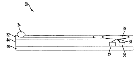
[0018] FIG. 2 is a diagram illustrating a sensor 30 according to an embodiment
of the present
invention. In FlG. 2, sensor 30 is a lateral flow biosensor. However, the
present invention is not
limited to being a °lateral flow" biosensor. Instead, the present
invention is applicable to
biosensors other than "lateral flow" biosensors. Moreover, the present
invention is not limited to
being a "biosensor". Instead, the present invention is applicable to many
different types of
sensors, including biosensors and chemical sensors.
[0019] Referring now to FIG. 2, sensor 30 includes a chemical layer 32. When
an analyte 34
is placed on chemical layer 32, an optical signal 38 is produced in zone 39 of
chemical layer 32.
For example, optical signal 38 is produced in response to a chemical or
physical modification of
analyte 34, or a chemical or physical modification of a chemical or material
in or on chemical
layer 32. A detector 36 detects signal 38, to thereby detect the presence,
absence or
concentration of analyte 34. For example, in some embodiments, the presence of
analyte 34
4
CA 02518633 2005-09-07
would be detected. In other embodiments, the concentration of analyte 34 would
be detected.
Detector 36 is placed in appropriate proximity to zone 39 to allow sufficient
detection of signal
38. Detector 36 is, for example, a photodiode. However, the present invention
is not limited to
detector 36 being a photodiode, and other suitable detectors can be used.
[0020] In some types of sensors, it is not required for the sensor to include
a light source. For
example, in some sensors, detector 36 may detect an absorption change in zone
39. Ambient
light might be sufficient for detector 36 to detect the change. If ambient
light is sufficient, it may
not necessary for the sensor to include a light source. Otherwise, a light
source might be
provided.
[0021] However, some sensors must include a light source. For example, some
sensors
require a light source to produce signal 38. As an example, a light source
might be required to
cause signal 38 to be produced via fluorescence .
[0022] If a light source is required to produce or detect signal 38, sensor 30
would include a
light source 42: Light source 42 is, for example, a light emitting diode
{LED). LEDs are well
known. However, light source 42 is not limited to being an LED, and other
suitable types of light
sources can be used.
[0023] Sensor 30 also includes a substrate 40. Substrate 40 includes
conductive elements
(not illustrated) to connect components together on substrate 40 or, if
necessary, to connect
external components to components on substrate 40. Substrate 40 is, for
example, a flexible
substrate such as, for example, a polyimide substrate. Such substrates are
well known.
However, substrate 40 is not limited to being a flexible substrate, and is
also not limited to being
a polyimide substrate. Instead, other suitable substrates can be used.
[0024] Detector 36 is on substrate 40. In the embodiment in FIG. 2, if sensor
30 also
includes light source 42, then light source 42 is also on substrate 40. For
example, detector 36
and light source 42 are bonded to substrate 40, or attached to substrate in
any suitable other
manner. Chemical layer 32 and substrate 40 are laminated together. In other
embodiments of
the present invention, detector 36 and light source 42 can be on opposite
sides of chemical layer
32. Hence, two optical layers (i.e., one layer including detector 36 and one
layer including light
source 42) are bonded to a chemical layer.
CA 02518633 2005-09-07
[0025] A separation layer 44 can be used to provide the necessary optical
separation
between chemical layer 32 and the optical components such as light source 42
and detector 36,
which is especially important when both light source 42 and detector 36 are
mounted on the
same side of chemical layer 32. For example, separation layer 44 can be
provided between
chemical layer 32 and substrate 40 so that separation layer 44 is between
chemical layer 32 and
detector 36, and between chemical layer 32 and light source 42. Separation
layer 44 can be, for
example, a separate piece of plastic or a clear, conformal coating on top of
substrate 40. Here,
"clear" indicates that separate layer 44 is "clear" to signal 38, and not
necessarily "clear" to the
human eye. For example, if light source 42 emits infrared light, separation
layer 44 might be
black in color to the human eye. Chemical layer 32, separation layer 44 and
substrate 40 are
laminated together.
[0026] By using an appropriate detector 36 (such as, for example, an surface
mount
photodiode), a suitable light source (such as, for example, an surface mount
LED), and a
suitable substrate (such as, for example, a polyimide flex substrate), the
present invention
integrates chemical layer 32, detector 36 and light source 42 together into
one unit, and can be
used, for example, as a disposable sensor. Such a disposable sensor would be
relatively
inexpensive compared to a conventional sensor. Further, such a disposable
sensor would have
substantial cost and size savings due to the lack of required submounts and
alignments as
compared to a conventional sensor. In addition, due to the proximity of
detector 38 to chemical
layer 32, a disposable sensor according to various embodiments of the present
invention might
not require any collection optics.
(0027] The integration of light source 42 and detector 36 on substrate 40 is
based, for
example, on flex technology. Generally, flex technology is typically used to
integrate electronic
components onto a flexible substrate. Flex technology is known, and has been
applied for low
cost manufacturing of a variety of electronic components such as, for example,
CMOS cameras.
For example, within conventional flex technology, the camera IC and any
required passive
components are directly mounted onto a flex substrate that is used to connect
the camera to a
PC board.
6
CA 02518633 2005-09-07
[0028] FIG. 3 is a diagram illustrating sensor 30 having an integrated display
device,
according to an embodiment of the present invention. Referring now to FIG. 3,
a display device
50 is on substrate 40. For example, display device 50 is bonded to substrate
40, or attached to
substrate in any suitable other manner. Display device 50 displays a result
corresponding to
signal 38 detected by detector 36. Display device 50 might, for example,
simply provide a light
which goes ON or OFF to indicate YES or NO. Or, display device 50 might, for
example, provide
a numerical readout con-esponding, for example, to the concentration of the
analyte. Display
device 50 is, for example, a light emitting diode (LED), an organic light
emitting diode (OLED) or
a liquid crystal display. However, display device 50 is not limited to being
an LED, an OLED or a
liquid crystal display, and any suitable display device can be used.
[0029] By using an appropriate display device 50 (such as, for example, an LED
or a liquid
crystal display), the present invention integrates chemical layer 32, detector
36, light source 42
and display device 50 together into one laminated unit, and can be used, for
example, as a
disposable sensor. Such a disposable sensor would be relatively inexpensive
compared to a
convention sensor using discrete components and a separate, external display
device.
[0030] Although not shown in FIGS. 2 and 3, appropriate components such as
polarizers,
optical filters and other measurement supporting components, can be integrated
into the optical
sensor to cooperate with light source 42 and/or detector 36, if desired. These
components can
be, for example, bonded to substrate 40, or provided as a layer between
chemical layer 32 and
substrate 40, and laminated together with chemical layer 32 and substrate 40.
The selection of
appropriate materials for such components would be within the skill of a
person of ordinary skill
in the art, in view of the disclosure herein.
[0031] According to embodiments of the present invention, if the appropriate
materials are
selected for use as light source 42, detector 36 and substrate 40, then light
source 42 and
detector 36 can be manufactured directly on substrate 40. For example, light
source 42 and
detector 36 can be made of organic materials (such as light source 42 being an
OLED and
detector 36 being an organic photodiode). Alternatively, detector 36 can be of
a material such
as, for example, amorphous silicon. In addition, substrate 40 can be, for
example, a flexible
substrate such as, for example, a polyimide substrate. With such material
selection, light source
42 and detector 36 can be manufactured directly on substrate 40. As a result,
the sensor can be
manufactured by a potentially low cost manufacturing method. The manufacturing
of a light
7
CA 02518633 2005-09-07
source such, for example, as an OLED on a substrate, such as, for example, a
flexible
substrate, is known. The manufacturing of a detector such as, for example, an
organic
photodiode or amorphous silicon, directly on a substrate, such as, for
example, a flexible
substrate, is known.
[0032] Although not shown in FIGS. 2 or 3, a power source would also typically
be provided
on the sensor. A power supply for integration in such a sensor would be
understood by a person
of ordinary skill in the art in view of this disclosure.
[0033] Moreover, although not shown in FIG. 3, a processing device might be
provided on
substrate 40 to process the output signal of detector 36 for use by display
device 50. A
processing device in such a sensor would be understood by a person of ordinary
skill in the art
in view of this disclosure.
[0034] Sensor 30 in FIGS. 2 and 3 is a lateral flow biosensor, since analyte
34 laterally flows
across chemical layer 32, which causes signal 38 to be produced in zone 39.
However, the
present invention also applies to sensors which are not lateral flow
biosensors.
[0035] For example, FIGS. 4 and 5 illustrate a sensor 60 according to
additional
embodiments of the present invention. Sensor 60 is not a lateral flow sensor
Referring now to
FIGS. 4 and 5, an analyte (not illustrated in FIGS. 4 and 5) is placed
directly in zone 39, to
thereby produce signal 38. Otherwise, sensor 60 in FIGS. 4 and 5 is similar to
sensor 30 in
FIGS. 2 and 3, respectively
[0036] In FIGS. 2-5, light source 42 and detector 36 are on the same side of
chemical layer
32 with respect to each other. However, in some embodiments, light source 42
and detector 36
can be on opposite sides of chemical layer 32 with respect to each other.
[0037] For example, FIGS. 6 and 7 illustrate a sensor having a light source
and detector on
opposite sides of chemical layer 32. Referring now to FIGS. 6 and 7, light
source 42 is provided
on a separate substrate 70. Substrate 70 might be, for example, a flexible
substrate such as, for
example, a polyimide substrate. However, substrate 70 is not limited to being
a flexible
substrate or a polyimide substrate. Chemical layer 32 is sandwiched between
substrates 40 and
70. Although separation layer 44 is shown in FIGS. 6 and 7, a separation layer
would often not
be necessary, and could be eliminated, if light source 42 and detector 36 are
on opposite sides
8
CA 02518633 2005-09-07
of chemical layer 32. Further, a display device, such as display device 50 in
FIGS. 3 and 5,
could be positioned on either substrate 40 or 70.
[0038] In FIGS. 6 and 7, substrate 70 is shown as being much shorter in length
than
substrate 40. The present invention is not limited to substrate 70 being any
specific length or
size with respect to substrate 40. In some embodiments of the present
invention, a window (not
illustrated) could be provided on substrate 70 to allow an analyte to be
passed through the
window and be placed on chemical layer 32.
[0039] There are many different types of sensors that operate in different
manners. The
present invention is not limited to any particular type of sensor The present
invention is
particularly applicable to biosensors and chemical sensors. Moreover, there
are many different
types of chemical layers or test strips that can be used in a sensor, and
these chemical layers or
test strips can operate with different underlying chemicals and in accordance
with different
mechanisms of action. The present invention is not limited to any particular
type of chemical
layer or test strip, to any particular underlying chemical, or to any
particular mechanism of action.
[0040 Although a few preferred embodiments of the present invention have been
shown ancf
described, it would be appreciated by those skilled in the art that changes
may be made in these
embodiments without departing from the principles and spirit of the invention,
the scope of which
is defined in the claims and their equivalents.
9