Note: Descriptions are shown in the official language in which they were submitted.
CA 02518687 2005-09-08
WO 2004/081588 PCT/US2004/007030
METHOD AND APPARATUS FOR DETECTING AND CORRECTING
WIRING ERRORS IN POWER MONITORING APPLICATIONS
~'hELD OF THE I1~~~1E~~T°I~I~t.T
This invention is directed generally to power monitoring, and more
particularly to
detecting and correcting wiring errors in power monitoring applications using
hardware-
based dynamic conversion means.
RACI~GROU~ID OF THE II~~1E1~TIOt~~
io Power monitoring systems monitor the flow of electrical power in circuits
through
a plant or other facility. In the POWERL~GIC~ system manufactured by the
instant
assignee, Square D Company, circuit monitors and power meters are dedicated to
power
monitoring, while other compatible devices collect additional equipment
information from
protective relays, circuit breakers, transformer temperature controllers, and
panelboards.
is Electrical data, such as current, power, energy, waveforms, and equipment
status, is
passed over a data network to one or more personal computers. The personal
computers
run power monitoring application software that retrieves, stores, organizes,
and displays
real-time circuit information in simple, usable formats. The information
collected and
stored in a power monitoring system helps operate a facility more efficiently.
The quality
ao of the data depends upon the accuracy of the instrumentation and the
usability of the
display formats.
The power meter can replace conventional metering devices such as ammeters,
voltmeters, and watt-hour meters while providing other capabilities not
offered by analog
metering. The power meter's true rms readings reflect non-linear circuit
loading more
is accurately than conventional analog metering devices. The power meter
calculates the
neutral current, which can assist in identifying overloaded neutrals due to
either
unbalanced single phase loads or harmonics. Circuits can be closely monitored
for
available capacity by keeping track of the peak average demand current.
Permanently installed electrical monitoring equipment is typically installed
during a
so plant shut-down which may only happen once or twice a year. ~ne or more
metering
devices are typically installed during these shutdowns. Upon re-energizing the
electrical
distribution equipment in the facility some wiring errors may be found that
cannot be
CA 02518687 2005-09-08
WO 2004/081588 PCT/US2004/007030
2
corrected until the next shut-down due to cost of taking manufacturing down to
correct
for these errors. In poly-phase systems, common wiring errors include swapping
phases
on the voltage and current channels or wiring current phases backwards. For
example,
the installer may mistakenly connect the phase B voltage line to the phase C
voltage line
s on a meter. I~ue to the differences in electrical connectors typically used,
interchanging
current and voltage lines is normally not encountered.
In somewhat more sophisticated or higher-end monitoring systems, a
microprocessor-based control system is utilized. In such systems, phase wiring
errors
may be corrected using software. However, this solution requires more
microprocessor
io processing time as well as at least double the memory requirement. That is,
buffers or
registers used to take in the raw data from the metering points or monitor
input would
have to be duplicated by a second buffer or register, in each instance, to
transfer the
corrected data points under control of the processor. In lower-end meiering
applications,
there is either insufFicient processing power, insufficient memory, or both to
correct phase
is wiring errors through software alone. Moreover, the analog circuitry which
processes
and digitizes the incoming signals is space-consuming.
Therefore, a need exists for a system and method for detecting and correcting
wiring errors without having to shut-down the system and without burdening the
processor with memory-intensive operations. A need also exists for a power-
monitoring
zo system having a reduced circuit board footprint. The present invention
satisfies this and
other needs.
SUMMARY OF THE INVENTION
Briefly, in accordance with the foregoing, a power-monitoring system that
detects
zs and dynamically corrects a wiring error in a poly-phase electrical circuit
includes inputs
adapted to receive power signals to be monitored, a processor having data
inputs, a
correction circuit including an analog multiplexes having inputs coupled to
receive the
power signals, having outputs coupled to said the inputs of the processor, and
having a
control input coupled to the processor, and the processor having a control
output coupled
3o with the control input to cause representative ones of the power signals to
be provided
CA 02518687 2005-09-08
WO 2004/081588 PCT/US2004/007030
from the outputs of the analog multiplexer to the data inputs of the processor
in a
determined sequence.
A method for detecting a wiring error in an electrical circuit monitored by a
power-monitoring system includes addressing an analog multiplexer under
control of a
s processor to select a first input carrying an analog voltage signal from the
electrical circuit
monitored by the power-monitoring system, addressing the analog multiplexes to
select a
second input carrying an analog current signal corresponding to the analog
voltage signal,
calculating the power factor corresponding to the analog voltage signal and
the analog
current signal, and comparing the power factor with an expected power factor
range.
io The above summary of the present invention is not intended to represent
each
embodiment, or every aspect, of the present invention. This is the purpose of
the figures
and the detailed description which follow.
BRIEF DESCRIPTION OF THE DRAWINGS
is The foregoing and other advantages of the invention will become apparent
upon
reading the following detailed description and upon reference to the drawings.
FIG. 1 is a functional block diagram of a poly-phase monitoring system;
FIG. 2 is a vectdr diagram of a three-phase power load with all phases in
their
correct relationship;
ao FIG. 3 is a vector diagram of a three-phase power load with two current
phases,
IB and IC, switched; ~,nd
FIG. 4 is a flo~.v chart diagram of the steps to obtain a power reading from a
three-
phase power circuit, in accordance with a specific embodiment of the present
invention.
While the invention is susceptible to various modifications and alternative
forms,
zs specific embodiments have been shown by way of example in the drawings and
will be
described in detail herein. It should be understood, however, that the
invention is not
intended to be limited to the particular forms disclosed. Rather, the
invention is to cover
all modifications, equivalents, and alternatives falling within the spirit and
scope of the
invention as defined by the appended claims.
CA 02518687 2005-09-08
WO 2004/081588 PCT/US2004/007030
4
DETAILED DESCRIPTION OF THE ILLUSTRATED EMBODIMENT
The present invention detects and corrects for wiring errors without requiring
the
electrical equipment to be powered down and rewired. There are at least two
common
wiring errors that operators can make when connecting electrical equipment to
power
s monitors. One wiring error involves swapping the phases on the current or
voltage lines,
such as connecting the phase A current line to the phase B current line. When
this wiring
error occurs, the displacement angles ofthe respective phases appear in the
wrong
quadrant. Another wiring error involves wiring up a current phase backwards,
such that
the current flows backwards with respect to its corresponding voltage phase.
io Generally speaking, in a three-phase system, typical power monitors provide
one
connection or metering point each for each of the three voltage and current
phases, for a
total of six connection points. Heretofore, basic metering devices would yield
incorrect
readings if the wrong phase is connected to the wrong input, for example, if
the phase-B
current line is physically connected to the phase-A current line. In such
systems, the only
is way in which to correct the error is to shut down the system and rewire the
metering
points as noted above.
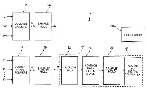
Referring to the drawings and initially to FIG. 1, there is shown the data
paths and
principal components of a poly-phase monitoring system 8 in accordance with an
embodiment of the present invention. The system 8 generally includes voltage
dividers
zo 10, current transformers 12, sample and hold circuits l4a,b, a correction
circuit 20, and a
processor 30. The correction circuit 20 includes a mufti-channel analog
multiplexes 22, a
common gainlfilter stage 24, a sample and hold circuit 26, and an analog-to-
digital
converter 28 (ADC).
N voltage lines and N current lines corresponding to 2N lines to be monitored
are
zs connected to the voltage dividers 10 and the current transformers 12. As is
known, the
voltage dividers 10 and current transformers 12 operate to reduce the
magnitude of the
incoming voltage and current, respectively, to levels appropriate for the
sample and hold
circuits l4a,b.
The voltage dividers 10 and the current transformer 12 are connected to N-way
3o sample and hold circuits 14a and 14b, respectively. The processor 30
simultaneously
strobes each of the sample and hold circuits l4a,b in order to obtain voltage
and current
CA 02518687 2005-09-08
WO 2004/081588 PCT/US2004/007030
samples of each input and to preserve the relative phase relationship of all
inputs of the
sample and hold circuits l4a,b.
In the correction circuit 20, the analog multiplexes 22 selects one of the N
voltage
or current charmels for analysis from at least 2N or ICI number of channels.
In a specific
s embodiment, the analog multiplexes 22 is an 8-channel multiplexes. An
optional neutral
line (not shown) may also be monitored by the system 8 and coupled to the
analog
multiplexes 22. Thus, in a three-phase system, 7 channels of the analog
multiplexes 22
would be used; 3 for each of the 3 voltage channels, 3 for each of the 3
current channels,
and one for neutral. Note that in other embodiments, a different number of
channels may
io be multiplexed by the analog multiplexes 22, which may have fewer or more
than 8
channels.
The selected channel is provided to the gain/filter stage 24 and the sample
and
hold circuit 26 and the resulting signal is converted to a representative
digital signal by the
ADC 28. In an embodiment, the ADC 28 is a 12-bit converter. The converted
digitized
is input is provided to the microprocessor for analysis. While a mufti-channel
ADC could be
used instead of the analog multiplexes 22, the conversion order would be fixed
and there
would only be a one-to-one mapping of the voltage and current channels. In
contrast, the
present invention utilizes the sample and hold circuits 14a and 14b in
conjunction with the
mufti-channel analog multiplexes 22 to dynamically change the conversion order
of the
zo channels by changing the successive addresses assigned to the analog
multiplexes 22 after
the sample and hold circuits 14 have latched the channels, such that the data
is always
provided to the processor in an expected order.
The analog multiplexes 22 is controlled through software executed by the
processor 30, which also controls the conversion order of the ADC 28 to
correct for any
as wiring errors without requiring the system 8 to be rewired. Any wiring
errors will be
detected by defaulting the conversion sequence to VA, VB, VC, IA, IB, IC or
the order
expected when the wiring is correct.
The correction circuit 20 may contain discrete elements or in other
embodiments
may be implemented in an integrated circuit such as the ADC12048 commercially
3o available from National Semiconductor. The integrated circuit replaces
numerous analog
components, which reduces complexity and circuit-board real estate.
CA 02518687 2005-09-08
WO 2004/081588 PCT/US2004/007030
6
FIG. 2 is a vector diagram of an exemplary three-phase power load with the
voltage phases VA, VB, and VC shown in proper phase relationship with their
corresponding current phases IA, IB, and IC. The power computation of a
polyphase
circuit is obtained by determining the po~r3rer factor using a Fast Fourier
Transform of each
s pair, i.e., VA/IA, VB/IB and VC/IC. The expected power factor associated
with each
phase is assumed to be within certain bounds, normally about 0.5 leading or
about 0.8
leading to about 0.5 lagging. When the phases have been wired up incorrectly,
one of at
least two things can occur. First, one or more of their associated
displacement angles
appear in the wrong quadrants. Thus, when two voltage lines are swapped, the
voltage
io phase appears 120 degrees out of the expected range. Second, current
appears to flow
backwards with respect to the voltage in the same phase. Thus, when a current
line is
wired up backwards, the phase for the current appears 180 degrees out of the
expected
range. To correct a current phase wired up backwards, the processor 30 is
instructed to
multiply the value corresponding to the current on the incorrectly wired up
phase by -1.
is FIG. 3 is a vector diagram of a three-phase power load with two current
lines, IB
and IC, inadvertently switched, i.e., the operator connected the phase-B
current line to
the phase-C current line. After performing a Fourier transform and analyzing
the phase
fundamentals of each phase, the processor 30 can determine that the operator
has
inadvertently switched the IB and IC lines. According to the present
invention, for any
zo wiring error in which phases are swapped (such as IB and IC swapped), the
A/D
conversion sequence for the power factor computation of each voltage/current
pair is
changed to VA/IA, VB/IC and VC/IB. The analog multiplexer 22, under control of
the
processor 30, switches the addresses of the incorrectly wired channels so that
they appear
to the processor 30 in the proper and expected order. The system 8 may inform
the
as operator that a wiring error has been detected and the type of wiring error
so that the
phases can be wired up correctly during the next planned system shutdown. The
present
invention avoids costly unplanned system shutdowns to correct wiring errors,
and does
not require substantial processor bandwidth or expanded memory allocation.
FIG. 4 depicts a flowchart for obtaining a power reading on a three-phase
(A,B,C)
so power circuit using the system 8 shown in FIG. 1. The main routine is
entered at step 100
which may occur by command or by a timer. At step 102, the N-way sample and
hold
CA 02518687 2005-09-08
WO 2004/081588 PCT/US2004/007030
7
circuits 14a and 14b are strobed by the processor 30 to obtain a snapshot of
the voltage
and current readings of the signals present in the voltage dividers 10 and the
current
transformers 12 at a specific instant of time.
At step 104, the power factor for phase A is determined by calling the power
s factor subroutine, steps 120-134, which is described in more detail below.
The power
factor subroutine returns the power factor for phase A, which may be stored in
a memory
location. This power factor A corresponds to the power factor for the
voltage/current
channel pairs from the voltage dividers 10 and the current transformers 12,
i.e., V1/I1.
At step 106, the power factor for phase B is determined in a similar manner,
io except that the parameter B is passed as an argument to the power factor
subroutine.° The
power factor B may also be stored in a memory location, and corresponds to the
power
factor for V2/I2.
At step 108, the power factor for phase C is determined by passing the
parameter
C to the power factor subroutine. The power factor C may be stored in a memory
is location, and corresponds to the power factor for V3/I3.
At step 110 the power of the three-phase circuit is calculated using the
computed
power factors for. phases A, B, and C. In an embodiment, the routine is idled
at step 112
until a timer restarts the cycle at step 100. In an alternate embodiment, the
routine
continually cycles, passing control from step 112 to step 100.
ao The power factor subroutine is initiated at step 120, and receives as
parameters
the addresses of the voltage/current pair (e.g., the address of Vl and the
address of Il) to
be analyzed. In one embodiment, the system 8 has already determined that one
or more
wiring errors has occurred, and instructs the multiplexer 22 to adjust the
addresses so that
the readings are made in the proper order. In another embodiment, such as at
power-up
as after the system 8 has been wired up, the system 8 has not yet determined
whether a
wiring error has occurred, and must therefore check the phase-angle
relationships of each
voltage/current pair to determine whether an adjustment in the analog
multiplexer 28 is
necessary. In yet another embodiment, the system 8 periodically or at
predetermined
intervals checks the phase relationships to verify they are not outside of
expected ranges.
so At step 122, tile analog multiplexer 22 selects the address of the voltage
line Vl-
VN corresponding to the phase parameter to be analyzed. For example, to
analyze phase
CA 02518687 2005-09-08
WO 2004/081588 PCT/US2004/007030
8
B, the address corresponding to voltage line V2 is selected by the multiplexer
22 under
command of the processor 30. If a wiring error has been previously detected, a
different
address may be selected. For example, if V1 and V2 were reversed, the address
of ~2
actually corresponds to the voltage line ~1. In such a case, the processor 30
would
s instruct the multiplexer 22 to select the address corresponding to voltage
line Vl in order
to compute the power factor for phase B.
As described in connection with FIG. 1, the multiplexer 22 receives the signal
corresponding to the voltage channel held by the sample and hold circuit 14a
and provides
the resulting signal to the gain/filter stage 24=. The amplified signal is
sampled by the
io sample and hold circuit 26 and digitized by the ADC 28. The digital signal
is provided to
the processor 30 in step 124. The resulting voltage sample may be stored in a
memory
location.
Similarly, at step 126 the processor 30 instructs the analog multiplexer 22 to
select
the address of the current line Il-IN corresponding to the phase parameter to
be analyzed.
is The analog multiplexer 28 reads the current channel corresponding to the
phase to be
analyzed from the sample and hold circuit 14b, and provides that signal to the
gain/filter
stage 24. The resulting signal is amplified and digitized by the ADC 28 and
provided to
the processor 30 in step 128. The resulting current sample may be stored in a
memory
location.
zo The processor 30 applies a Fast Fourier Transform algorithm on the voltage
and
current samples to obtain their phase angles. At step 130, the processor
optionally checks
the relationship of the phase angles. As noted above, the expected power
factor on each
phase is assumed to be within certain bounds, normally about 0.5 leading or
about 0.8
leading to about 0.5 lagging. If the relationship is outside of an expected
range, then a
zs wiring error or other circuit failure may be indicated.
In the preceding description, the addresses of the voltagelcurrent pairs is
assumed
and those addresses are passed to the power factor routine steps 120-134 as
arguments.
In the case of a wiring error, the error can be detected at optional step 130
and a new
current line address I1-IN can be tried until a reading is obtained indicating
a proper phase
3o relationship. In such a case, the addresses of the voltage/current pairs
are modified such
that the voltage/current phases are in their proper relationship. For example,
in the wiring
CA 02518687 2005-09-08
WO 2004/081588 PCT/US2004/007030
9
error described in connection with FIG. 3, steps 104, 106, 108 would call the
power
factor routine with the voltage/current address arguments of Vl/I1, V2/I3 and
V3/I2
respectively. In this manner, although the IZ and I3 lines are swapped, the
data
nonetheless arrives in the menl~ry map in the e:~pected sequence. The power
factor
s subroutine is exited at step 134.
The invention generally may be used in meters or other devices which monitor
electricity or quantities with known phase relationships such as power
systems. The
invention offers greater flexibility in auto configuration or self correction
for wiring errors
without causing downtime to the end user. While a 3-phase power system has
been
io described herein, it is understood that the system 8 can be extended to any
number of
inputs which have fixed phase relationships.
As indicated above, the invention may have other uses or advantages as well.
For
example, rather than correcting for incorrect wiring sequences, the invention
may be used
to automatically configure any given wire sequence to a desired input sequence
and any
is type of metering or monitoring situation where the quantities to be
monitored have known
phase or relationships which can be detected by the monitoring process. In
addition, the
invention advantageously can solve for problems of coupling between channels.
While particular embodiments and applications of the present invention have
been
illustrated and described, it is to be understood that the invention is not
limited to the
ao precise construction and compositions disclosed herein and that various
modifications,
changes, and variations may be apparent from the foregoing descriptions
without
departing from the spirit and scope of the invention as defined in the
appended claims.