Note: Descriptions are shown in the official language in which they were submitted.
CA 02518955 2008-02-11
TITLE OF THE INVENTION
COATED ARTICLE INCLUDING TITANIUM OXYCARBIDE AND
METHOD OF MAKING SAME
[0001] This application relates to a coated article including a layer
comprising
titanium oxycarbide, and a method of making the same. In certain example
embodiments, a layer of titanium oxide (e.g., TiOx, where x is from 1 to 3,
preferably
about 2) is sputter deposited on a substrate; and thereafter an ion source(s)
using a
high voltage is used to implant carbon (C) ions with high energy into the
titanium
oxide so as to form a layer comprising titanium oxycarbide.
BACKGROUND OF THE INVENTION
[OOU2] Contact angle 0 in general is discussed in U.S. Patent Nos. 6,303,225
and 6,461,731. In certain instances, high contact angles are desired, while in
other
instances low contact angles are desired. The desired contact angle depends
upon the
situation in which an intended product is to be used.
[0003] It is known in the art to coat a glass substrate with a layer of
titanium
oxide (e.g., Ti02, or other stoichiometry). A layer of titanium oxide, if
provided as
the outermost layer on a glass substrate, can achieve a rather low contact
angle 0 with
a sessile drop of water after lengthy exposure to ultraviolet (UV) radiation
and water.
[0004] However, titanium oxide layers are problematic with respect to
durability. For example, the scratch resistance of a titanium oxide layer is
not that
much better than that of glass. As a result, coated articles with an exposed
layer of
titanium oxide are highly susceptible to damage (e.g., scratching) during
transport and
the like, and are problernatic ui this respect.
[0005] In view of the above, it is apparent that there exists a need in the
art for
a coated article that is more durable (e.g., scratch resistant) than is pure
titanium
oxide. In certain example instances, a low contact angle 0 may also be
desired.
1
CA 02518955 2005-09-12
WO 2004/081251 PCT/US2004/007054
BRIEF SUMMARY OF EXAMPLE EMBODIMENTS
[0006] According to certain example embodiments of this invention, a coated
article is provided which includes a layer comprising titanium oxycarbide
and/or
titanium carbide. In order to forrn the coated article, a layer corxbprising
titanium
oxide (e.g., TiO%, where x is from 1 to 3, preferably about 2) is deposited on
a
substrate by sputtering (e.g., magnetron sputtering) or any other suitable
deposition
technique. Other layer(s) may or may not be provided between the substrate and
the
layer comprising titanium oxide in different embodiments of this invention.
After
sputtering of the layer comprising TiO, an ion beam source(s) is used to
implant at
least carbon ions into the TiO$. When implanting into the TiO$ inclusive
layer, the
carbon ions have sufficient ion energy to penetrate the surface of the layer
and knock
off oxygen (0) atoms from TiO,, molecules so as to enable a substantially
continuous
layer comprising titanium oxycarbide to form near a surface of the previously
sputtered layer. In embodiments where the sputtered TiO,, layer is
sufficiently thick,
the layer comprising titanium oxycarbide may be formed over a layer of TiOX
which
was originally a lower portion of the originally sputtered TiOx layer.
[0007] A relatively high voltage is required in the ion source(s) in order to
provide sufficient energy for the carbon ions from the ion source to: (a)
penetrate the
surface and implant into the sputtered TiOX layer, (b) knock off oxygen from
TiOx
molecules, and (c) carry out (a) and (b) to an extent sufficient so that a
substantially
continuous layer of titanium oxycarbide can be formed. In order to achieve
sufficient
energy in this respect, according to certain example embodiments of this
invention the
ion source(s) uses an anode-cathode voltage of at least about 800 V, more
preferably
of at least about 1,500 V, even more preferably of at least about 2,000V, and
still
more preferably of at least about 2,500 V. For purposes of example only, in
the case
where the C ions are formed using acetylene (C2H2,) as a feedstock gas in an
ion
source, the aforesaid ion source voltages translate into respective ion
energies of at
least about 200 eV per C ion, more preferably at least about 375 eV per C ion,
even
more preferably at least about 500 eV per C ion, and still more preferably of
at least
about 625 eV per C ion.
2
CA 02518955 2005-09-12
WO 2004/081251 PCT/US2004/007054
[0008] In certain example embodiments, C ions are implanted deep enough
into the sputtered TiOX layer so as to enable a substantially continuous layer
comprising titanium oxycarbide to form at least at a top portion thereof. This
layer
comprising titanium oxycarbide may include TiO, TiC, TiOC, OC, CC, CH, and/or
combinations thereof. In certain example embodiments, at least some C ions (or
C
atoms) are implanted into the sputtered layer to a depth "d" of at least 25 A
below the
top surface of the sputtered layer (more preferably at least 50 A, even more
preferably
e
at least 100 A).
[0009] The coated article made, as explained above, to include a layer
comprising titanium oxycarbide has improved scratch resistance compared to
that of a
purely titanium oxide layer. Moreover, in certain example embodiments, the use
of C
implantation enables certain contact angle 0 characteristics to be improved.
For
example, the resulting coated article may be capable of achieving lower
contact
angles 0, (initial, or after UV/water exposure) than a layer of pure amorphous
diamond-like carbon (DLC) and/or a layer of pure titanium oxide. The resulting
coated article may also be capable of maintaining a low contact angle(s) 0 for
a longer
period of time than a layer of titanium oxide. Thus, it can be seen that the
implantation of C ions/atoms into the layer comprising titanium oxide is
advantageous
in several respects.
[0010] Optionally, in addition to the C ions which are implanted into the
layer
comprising titanium oxide to form the titanium oxycarbide, further ion beam
deposition of carbon using high ion energy may take place over the titanium
oxycarbide in certain example embodiments so that a thin layer comprising
amorphous diamond-like carbon (DLC) with a large amount of sp3 carbon-carbon
bonds (e.g., at least 40% such bonds, more preferably at least 50% such bonds)
may
0
be formed over the oxycarbide. This additional DLC layer may be from 0 to 100
A
thick in certain example embodiments of this invention, more preferably from 1
to 40
A thick, and most preferably from about 1 to 30 OA thick. This optional DLC
layer
may or may not be hydrogenated (e.g., from about 1-25% H, more preferably from
about 3-18% H) or include other dopants in different embodiments of this
invention,
and may have a density of at least 2.4 gms/cm3 in certain example instances.
This
3
CA 02518955 2005-09-12
WO 2004/081251 PCT/US2004/007054
DLC inclusive layer may serve to improve durability in certain example
embodiments
of this invention.
[0011] In certain example embodiments of this invention, there is provided a
method of malging a coated article, the method comprising: providing a glass
substrate; sputtering a layer comprising titanium oxide 'I`iO" (where x is
from 1 to 3)
on the substrate, thereby forming a sputtered layer; and utilizing at least
one ion
source using anode-cathode voltage of at least about 1,500 V to cause at least
carbon
ions to be directed toward the sputtered layer comprising titanium oxide so
that at
least some of the carbon ions are implanted into the sputtered layer to a
depth of at
least 25 A below a surface of the sputtered layer.
[0012] In other example embodiments of this invention, there is provided a
method of making a coated article, the method comprising: providing a
substrate;
forming a layer comprising a metal oxide on the substrate; and directing at
least
carbon ions toward the layer comprising the metal oxide, at least some of the
carbon
ions having an ion energy of at least 200 eV per carbon ion so that at least
some of the
carbon ions implant in the layer thereby forming a layer comprising an
oxycarbide.
[0013] In other example embodiments of this invention, there is provided a
coated article comprising a coating supported by a substrate, the coating
comprising: a
sputtered layer comprising a metal oxide, and at least carbon atoms which are
ion
beam implanted in the sputtered layer comprising the metal oxide, at least
some of the
carbon ions being implanted to a depth of at least 25 A below a surface of the
sputtered layer, thereby forming a layer comprising an oxycarbide.
BRIEF DESCRIPTION OF THE DRAWINGS
[0014] FIGURE 1 is a schematic partial cross sectional view illustrating a
technique for making a coated article according to an example embodiment of
this
invention.
[0015] FIGURE 2 is a flowchart illustrating certain steps performed in making
the article of Fig. 1 according to an example embodiment of this invention.
4
CA 02518955 2005-09-12
WO 2004/081251 PCT/US2004/007054
[0016] FIGURE 3 is a sectional view of an example ion source which may be
used to implant carbon ions into the originally sputtered titanium oxide
inclusive layer
of Figs. 1-2 according to an example embodiment of this invention.
[0017] FIGURE 4 is a perspective view of the ion source of Fig. 3.
[0013] FIGURE 5 is an ~TS (X-ray Photoelectron Spectroscopy) graph
illustrating the elements/components present in atomic amounts throughout the
thickness of the layer system of Example 1 at a first location on the
substrate.
[001.9] FIGURE 6 is an XPS graph illustrating the elements/components
present in atomic amounts throughout the thickness of the layer system of
Example 1
at a second location on the substrate (different than the first location
measured in Fig.
5).
[0020] FIGURE 7 is a time vs. contact angle 8 graph comparing a sputtered
layer of only Ti02 to sputtered Ti02 implanted with and/or covered with
different
amounts of C.
DETAILED DESCRIPTION OF EXAMPLE EMBODIMENTS OF THE
INVENTION
[0021] Certain embodiments of the instant invention relate to a coated article
which includes a layer comprising titanium oxycarbide. In order to form the
coated
article in certain example embodiments, a layer of titanium oxide (e.g., TiO,,
where x
is from 1 to 3, more preferably from 1.5 to 2.5, and most preferably about 2)
is
deposited on'a substrate by sputtering (e.g., magnetron sputtering) or via any
other
suitable deposition technique. Other layer(s) may or may not be provided
between the
substrate and the titanium oxide in different embodiments of this invention.
After
sputtering of the layer comprising TiOX, at least one ion beam source is used
to
implant carbon (C) ions into the TiO$. When implanting into the Z'iOY layer,
the
carbon ions have sufficient ion energy so as to penetrate the surface of the
sputtered
layer, and knock off oxygen (0) from TiO, molecules so as to enable a
substantially
continuous layer comprising titanium oxycarbide to form near a surface of the
previously sputtered layer. In embodiments where the sputtered TiO,, layer is
CA 02518955 2005-09-12
WO 2004/081251 PCT/US2004/007054
sufficiently thick, the layer comprising titanium oxycarbide may be formed
over a
layer of TiO, which was originally a lower portion of the originally sputtered
TiO,,
layer.
[0022] The coated article including at least one substantially continuous
layer
comprising titanium oxycarbide has improved scratch resistance compared to
that of a
purely titanium oxide layer. Moreover, in certain example embodiments the use
of
the C implantation enables certain contact angle 0 characteristics to be
improved. For
example, it has been found that the resulting coated article may be capable of
achieving lower contact angles 0(initial, or after UV/water exposure) than
would a
layer of pure amorphous diamond-like carbon (DLC) and/or a layer of pure Ti02.
Surprisingly, the resulting coated article may also be capable of maintaining
a low
contact angle(s) 0 for a longer period of time than would a layer of only
titanium
oxide. Thus, it can be seen that the implantation of C ions/atoms into the
layer
comprising titanium oxide is advantageous in several significant respects.
[0023] Coated articles herein comprising an oxycarbide, may be used in
various commercial applications, including but not limited to insulating glass
(IG)
window units, vehicle windows, architectural windows, furniture applications,
and/or
the like.
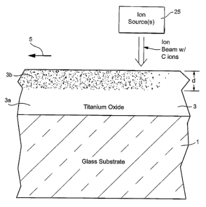
[0024] Fig. 1 is a cross sectional view of a coated article being formed
according to an example embodiment of this invention, whereas Fig. 2 sets
forth steps
that are carried out in making the coated article of Fig. 1. Referring to
Figs. 1-2, a
substrate (e.g., glass substrate which may or may not include other layers) is
provided
(see step A in Fig. 2). An amorphous layer 3 of or including titanium oxide
(TiOr) is
then deposited by sputtering on the substrate (see step B in Fig. 2). The
sputtered
titanium oxide of layer 3 may or may not be doped with other elements in
different
embodiments of this invention. Layer 3.~nay be from about 50 to 1,000 A thick
in
certain example embodiments of this invention, more preferably from about 50
to 500
A thick. After the TiO% inclusive layer 3 has been sputtered onto substrate,
the coated
article is moved in direction 5 as shown in Fig. 1 relative to at least one
ion source 25.
At least one gas including carbon (e.g., a hydrocarbon gas such as C2I~~ or
the like) is
fed through or used in the ion source(s) so that the ion source(s) 25 causes
an ion
6
CA 02518955 2005-09-12
WO 2004/081251 PCT/US2004/007054
beam including carbon (C) ions to be emitted toward the TiOx inclusive layer 3
(see
step C in Fig. 2). The C ions in the ion beam are provided with sufficient
energy so
that they can implant into the TiO, inclusive layer 3 as shown in Fig. 1. In
Fig. 1, the
dots illustrated in layer 3 represent C ions/atoms that have implanted into
the
sputtered layer 3; and the far right-hand portion of the layer 3 in Fig. 1 has
no
implanted dots because that portion of the coated article has not yet passed
under the
ion source. It is noted that the ion beam from source 25 may be focused,
diffused, or
collimated in different embodiments of this invention.
[0025] The implantation of C ions/atoms into the sputtered TiO, inclusive
layer 3 causes a layer comprising titanium oxycarbide 3b to be formed at least
proximate the surface of the layer as shown in Fig. 1 (see also step D in Fig.
2). This
implantation of C ions/atoms into layer 3 causes the durability of the
resulting layer to
significantly improve relative to that of layer 3 before the C ions/atoms were
implanted. For example, scratch resistant is significantly improved.
[0026] Moreover, it has surprisingly been found that the presence of the
implanted carbon in the layer 3 enables the resulting amorphous layer's
contact angle
0 to be fairly low in certain instances relative to pure titanium oxide. For
example,
Fig. 7 illustrates that the implanted layer 3 can realize a lower initial
contact angle 0
than can a layer of only amorphous titanium oxide. Thus, one does not
necessarily
need microcrystalline Ti02 (anatase or rutile) to induce low contact angles in
a
titanium oxide inclusive layer. Moreover, it has surprisingly been found that
once the
C ions/atoms have been implanted in layer 3, and a low contact angle has
been
achieved, the layer's ability to maintain a low contact angle(s) 0 over time
is
significantly improved compared to the situation where the C ions/atoms were
not
implanted (see Fig. 7). Yet another surprising aspect of certain example
embodiments
of this invention is that the implantation of the C ions/atoms into layer 3
enables the
implanted layer to realize hydrophilic behavior (low contact angle(s)) in the
presence
of green visible light without necessarily needing UV to induce lower contact
angles).
In other words, visible green light for example may cause the contact angle of
the
implanted layer to decrease which is advantageous in many commercial
situations.
7
CA 02518955 2005-09-12
WO 2004/081251 PCT/US2004/007054
[0027] In certain example embodiments of this invention, the layer comprising
titanium oxycarbide has a contact angle 0 of no greater than about 20 degrees,
more
preferably no greater than about 15 degrees. This contact angle may be either
an
initial contact angle, or after exposure to UV radiation and water (QUV) for
at least
50 hours. The QUV exposure is known in the art.
[0023] When implanting into the TiO, layer, the carbon ions have sufficient
ion energy so as to knock off oxygen (0) from TiO,, molecules so as to enable
a
substantially continuous layer comprising titanium oxycarbide 3b to form near
a
surface of the previously sputtered layer as shown in Fig. 1. Fig. 1 also
illustrates an
embodiment where the sputtered TiO$ layer 3 was sufficiently thick so that the
layer
comprising titanium oxycarbide 3b (in the area of the implanted dots shown in
Fig. 1)
may be formed over a layer of TiOr 3a which was originally a lower portion 3a
of the
originally sputtered TiO,, layer. In certain example embodiments, the titanium
oxycarbide layer 3b may be characterized at least in part by TiO,Cy, where x/y
is from
0.5 to 1.5.
[0029] It is also believed that the implantation of the C ions/atoms into the
layer 3 as shown in Fig. 1 can cause a heterojunction to occur between
resulting layers
3a and 3b. This heterojunction is formed at the interface between layers 3a
and 3b (or
alternatively at the interface between semiconductive layer 3b and an
overlying
semiconductive layer comprising DLC), these layers having different bandgaps
(TiOX
is about 3.2 eV +/- about 0.1, and the DLC may have a bandgap of about 1.9 to
2.2
eV). Under chemical equilibrium conditions, the fermi levels are aligned in
the two
materials, so that band bending may occur. This band bending creates an
internal
field at the heterojunction. Charge accumulates at the interface. It is
believed that
when incident light (e.g., visible green light) hits this charge at the
heterojunction,
electron hole pairs form and cause contact angle 0 to decrease.
[0030] A relatively high voltage is required in the ion source(s) 25 in order
to
provide sufficient energy for the carbon ions in the beam from the ion source
to: (a)
implant into the sputtered TiO, layer 3, (b) knock off oxygen from TiO,
molecules,
and (c) carry out (a) and (b) to an extent sufficient so that a substantially
continuous
layer of titanium oxycarbide 3b can be formed. In order to achieve sufficient
energy
8
CA 02518955 2005-09-12
WO 2004/081251 PCT/US2004/007054
in this respect, according to certain example embodiments of this invention
the ion
source(s) 25 uses an anode-cathode voltage of at least about 800 V, more
preferably at
least about 1,500 V, even more preferably at least about 2,000V, and still
more
preferably at least about 2,500 V. Even a source voltage of at least about
3,500 V
may be used in certain instances.
[0031] The aforesaid "voltage" (or accelerating voltage) referred to which is
used in the ion source(s) 25 to cause implantation of the C ions/atoms in
layer 3, is the
voltage between the anode and the cathode of the ion source 25. As is known in
the
art, "ion energy" is related to this anode/cathode "voltage" but is different
therefrom.
The molecular fragment ion energy is one half (1/2) of the accelerating
voltage for
molecular acetylene (C2H2) for example. Thus, the molecular fragment ion
energy,
given a voltage of 2,000 V would be 2,000/2 = 1,000 V. Moreover, in the case
of C
ions formed from acetylene (C2H21) used as a feedstock gas in the ion source,
there are
two carbon atoms per molecular fragment. Thus, the energy per carbon ion is
the
molecular fragment ion energy divided by 2 in this case where C2H2 is used as
the
feedstock gas to form the C ions in the beam. In other words, for purposes of
example only, in the case where the C ions are formed using C;,Hz as the
feedstock
gas in the ion source 25, ion source voltages (i.e., at least about 800 V,
1,500 V, 2,000
V and/or 2,500 V as explained above) translate into ion energies of at least
about 200
eV per C ion, more preferably at least about 375 eV per C ion, even more
preferably
at least about 500 eV per C ion, and still more preferably at least about 625
eV per C
ion.
[0032] In certain embodiments of this invention, it is important that one or
more of the aforesaid ion source voltages and/or ion energies be used. This is
because, if too low of an ion energy (or voltage in the ion source 25) is used
(e.g., 75
eV per C ion is too low), C ion implantation and/or formation of a continuous
layer
comprising titanium oxycarbide cannot be achieved.
[0033] It will be recognized that when a hydrocarbon gas such as C2H2 is used
as the feedstock gas in the source 25, the ions in the resulting beam will
include both
C ions and H ions. Thus, the titanium oxycarbide layer 3b may be doped with H
in
certain embodiments of this invention. In certain example embodiments, the
layer 3b
9
CA 02518955 2008-02-11
may include from 0 to 20% H, more preferably from about L to 18% H, and even
more preferably from about 5 to 15% H. Other materials may also be present in
layers 3a, 3b in certain instances, as shown in the XPS graphs discussed
herein.
[0034] In certain embodiments of this invention, C ions are implanted deep
enough into the sputtered TiO, layer 3 so as to enable a substantially
continuous layer
comprising titanium oxycarbide 3b to form at [cast proximate a top portion
thereof.
In certain example embodiments, at least some C ions (and/or C atoms) are
implanted
into the sputtered layer 3 to a depth "d" of at least 25 A below the top
surface of the
sputtcred layer (more preferably at least 50.8-, even more preferably at least
100 A).
Insufficient implantation may contribute to non-enhancement of durability, or
the like,
or very quick wearing off of the same.
[0035] In certain example embodiments of this invention, the ion source(s) 25
may be operated so as to only emit enough C'sons toward layer 3 so as to cause
C
ion/atom implantation in layer 3 as shown in Fig. 1, but not to cause a layer
of
amorphous DLC (e.g., ta-C or ta-C:H) to form over the titanium oxycarbide
layei- 3h.
Alternatively, in other embodiments of this invention, the source(s) 25 is
operated so
as to cause a thin laycr (not shown) comprising amorphous DLC (e.g., ta-C or
ta-C:Fi)
to form ovcr the titanium oxycarbide layer 3b. Example characteristics of such
DLC
layers are discussed in U.S. Patent No. 6,261,693. This thin DLC layer may be
from
about 1-30 A thick in certain example embodiments, more preferably from about
1-20
A thick. tt is noted that other layers may also be provided over the
oxycarbide in
certain instances. Moreover, this very thin DLC inclusive layer may in certain
embodiments be sacrificial in that it is designed so that it may wear away
(i.e.,
disappear) over time. Thus, for example, such a thin layer comprising DLC may
be
used to protect the coated article from scratching or the like during
shipping, process,
or the like, and then wear off over time so as to expose the layer comprising
titanium
oxycarbide 3b which may be characterized by a more desirable low contact angle
and/or good durability. It is also noted that in certain example embodiments,
the
titanium oxycarbide may be designed tu be sacrificial, so that it wears away
over time
after its job of protecting the coating from scratching or the like during
shipmeut,
processing, or the like, has been fulfilled.
CA 02518955 2005-09-12
WO 2004/081251 PCT/US2004/007054
[0036] Optionally, this overlying layer comprising DLC may be even thicker
than 30 A in certain example instances. Such overlying DLC inclusive layer(s)
herein
may include a large amount of sp3 carbon-carbon bonds (e.g., at least 40 ' of
C-C
bonds in the layer may be such bonds, more preferably at least 50%), may or
may not
be hydrogenated (e.g., from about 1-25% H, more preferably from about 3-18~'
H) or
include other dopants in different embodiments of this invention, and/or may
have a
density of at least 2.4 gms/cm3 in certain example instances.
[0037] Figs. 3-4 illustrate an example ion source 25 which may be used to
implant C ions in layer 3 according to certain example embodiments of this
invention.
Ion source 25 includes gas/power inlet 26, anode 27, grounded cathode magnet
portion 28, cathode magnet portion 29, and insulators 30. A 3kV (or other
power
supply amount) DC and/or AC power supply may be used for source 25 in some
embodiments. The voltages described above are provided between the anode 27
and
the cathode 29 of the ion source proximate the electric aap near the racetrack
shaped
slit in the cathode. Ion beam source 25 is based upon a known gridless ion
source
design. The linear source includes a linear shell (which is the cathode and
may be
grounded) inside of which lies a concentric anode (which is at a positive
potential).
This geometry of cathode-anode and magnetic field 33 gives rise to a closed
drift
condition. The source can also work in a reactive mode. The source may
includes a
metal housing with a slit in a shape of a race track as shown in Figures 3-4,
the hollow
housing being at ground potential in example instances. The anode electrode 27
is
situated within the cathode body 28, 29 (though electrically insulated) and is
positioned just below the slit. The anode 27 can be connected to a positive
potential
as high as 3,000 or more volts (V) (or as otherwise needed for the varying ion
energies used herein). Both electrodes may be water cooled in certain
embodiments.
One or more feedstock or precursor gas (e.g., acetylene, other hydrocarbon
gas, or any
other suitable gas) is/are fed through the cavity between the anode and
cathode (or
alternatively may be otherwise provided at the source).
[0033] Still referring to Figs. 3-4, electrical energy cracks the gas(es) to
produce a plasma within the source 25. The ion beam emanating from the slit is
approximately uniform in the longiludinal direction and has a Gaussian profile
in the
11
CA 02518955 2008-02-11
transverse direction. Exemplary ions 34 in the ion beam are shown in Figure 3.
A
source as long as four meters may be made, although sources of different
lengths are
anticipated in different embodiments of this invention. Electron layer 35
completes
the circuit thereby enabling the ion beam source to function properly. The ion
beam
source of Figs. 3-4 is merely exemplary. Thus, in altemative embodiments of
this
invention, an ion beam source device or apparatus as described and shown in
the first
three flgures of U.S. Patent No. 6,002,208 may be used. Any other suitable
type of
ion source may also be used.
[0039] In certain embodiments, the oxycarbide may be heated during and/or
after the ion beam treatment, from for example from about 100 to 650 degrees
C.
This heating may make the surface more hydrophilic, and/or to enhance the
formation
of oxvcarbides.
EXAMPLES
[0040] For purposes of example only, several examples were made and
analyzed in accordance with different embodiinents of this invention. In each
of the
below-listed examples, an amorphous TiOz layer 3 approximately 220-230 A thick
was magnetron sputtered onto a 3 mm thick glass substrate 1. 1'hen, cach
sample was
passed beneath an ion source 25 at a rate of 100 inches per minute, where the
source
25 used acetylene gas to expel at least C ions toward the layer 3. The beam
was
incidcnt on the layer 3 at an angle of about 90 degrees. In Example 1, the
layers were
deposited on the tin side of the Ãfoat glass substrate 1, whereas in Examples
2-4 the
lavers were deposited on the air side (non-tin side) of the substrate 1.
Processing for
the implantation for each example is set forth below. Gas flows bclow are
total gas
flows of acetylene in units of scem in the sourcc, and voltage is the
anode/cathode
voltage in'source 25.
TABLE I: iMPLANTATION PROCESSING FOR EXAMPLES
Gas & Flow Voltage CtuTent Pressure
Example I: C2H2 100 sc:cm 4,500 V 0.87 A 0.30 mTorr
12
CA 02518955 2005-09-12
WO 2004/081251 PCT/US2004/007054
Example 2: C2H2 100 sccm 3,000 V 0.79 A 0.32 mTorr
Example 3: C2H2 120 sccm 3,000 V 1.01 A 0.35 mTorr
Example 4: C2H2 310 sccm 3,000 V 1.17 A 0.99 mTorr
[0041] Example 1 was analyzed via ~TS, at two different locations illustrated
in Figs. 5 and 6. In the XPS analysis, 15 A steps were used. Fig. 5 is an XPS
graph
illustrating the elements/components present in atomic amounts throughout the
thickness of the layer system of Example 1 at a first location on the
substrate, where
in the graph the vertical axis represents atomic percent while the horizontal
axis
represents the depth into the coating from the exterior surface thereof in
units of
angstroms (A) relative to sputtering of a silicon oxide layer as is known in
the art.
Fig. 6 is similar to Fig. 5, except that the data was measured at a different
location on
the Example 1 sample. The instrument used for the measuring was a Physical
Electronics Quantum 2000 Scanning XPS, and the x-ray source was monochromatic
Al Ka. The analysis area was 0.2 mm by 0.2 mm, and the take-off angle was 45
degrees. Sputter conditions used for the reference thickness were 1 keV Ar+, 2
mm x
2 mm raster, - 30A/min vs. Si02.
[0042] As shown in Figs. 5-6, on the surface the proportion of C-O relative to
C-C/C-H appears to be similar in both areas. The Ols spectra reflects a
mixture of
metal oxides and hydroxide/organic. Moreover, it is noted that the coating
thickness
appears to be smaller in the location of Fig. 5 than in the location of Fig. 6
(the
increase in Si content in Figs. 5-6 is indicative of the presence of the glass
substrate
under the coating). The Cls spectra in the depth profile in Fig. 5 do not
reveal the
presence of TiC per se, rather it suggests an intermediate species of C in the
matrix of
TiOr (i.e.,. titanium oxycarbide), possibly bonded to both Ti and O(again,
titanium
oxycarbide). Thus, the phrase "titanium oxycarbide" as used herein includes
TiOC
bonding, and also situations where C is provided in a matrix of TiO,, but need
not
necessarily be bonded thereto.
[0043] Unfortunately, severe peak interference in the Ti2p spectra prevented
differentiation of TiC and TiO, which have nearly the same binding energy; and
also
13
CA 02518955 2005-09-12
WO 2004/081251 PCT/US2004/007054
precluded differentiation of various oxidic states due to Ti2p3 and Ti2pl
spectra
interference. This leads us to use two labels for Ti, elemental Ti and
TiOXCy/TiC. In
Fig. 5, a significant proportion of Ti appears to be in elemental state near
the glass
substrate 1 interface, and not much TiC was observed judging from the lack of
C-Ti
peak in the Cls spectra. In contrast, C-Ti bonding was indeed present in the C
ls
spectra in Fig. 6 and it peaked at about 50 A. The intermediate species of C
in the
matrix of TiO$, as mentioned above, was also present in the Cls spectra in
Fig. 6.
Fig. 6 also illustrates a higher TiO,,Cy/TiC concentration around 50 A, and
significant
titanium oxycarbide in this respect all the way through the layer 3, implying
a fairly
uniform distribution of the titanium oxycarbide component. In Fig. 6,
elemental Ti
was present in the film except for the top 50 A. The film of Example 1 was
also
found to have a very low contact angle, which angle decreased upon exposure to
visible light, and superior scratch resistance compared to titanium oxide.
[0044] Fig. 7 is a graph comparing Example 2 (Ti02 + C implant) vs. both a
layer of only Ti02 on a substrate and a layer of C implanted TiOz coated with
a layer
of DLC about 40 A thick over the same. It can be seen that the coated article
of
Example 2 had lower initial contact angle than either of the other two
articles, which
is advantageous in certain instances. Moreover, Fig. 7 illustrates that
Example 2 was
able to maintain a low contact angle for a longer period of time than were the
other
two samples.
[0045] While the invention has been described in connection with what is
presently considered to be the most practical and preferred embodiment, it is
to be
understood that the invention is not to be limited to the disclosed
embodiment, but on
the contrary, is intended to cover various modifications and equivalent
arrangements
included within the spirit and scope of the appended claims.
14