Note: Descriptions are shown in the official language in which they were submitted.
CA 02519932 2005-09-20
WO 2004/102820 PCT/CA2004/000733
Peak Current Control in Wireless Network Interface Devices
FIELD OF THE INVENTION
[0001] The present invention relates generally to current control in
electrical
devices. More particularly, the present invention relates to peak current
control in
wireless network interface devices such as, for example, wireless modems.
BACKGROUND OF THE INVENTION
[0002] Communication devices, such as cellular telephones, allow voice
communications over wireless coznrnunications networks. Such devices have
become
commonplace in today's world. In recent years, efforts have been made to
leverage
existing wireless communication systems, so that not just voice information
may be
communicated, but so that data from, for example, a portable (i.e. laptop)
computer or
personal digital assistant (PDA) may also be transmitted over the wireless
networks. One
result of such efforts is the General Packet Radio Service (GPRS) standard,
which
provides a packet switched data overlay of the Global System for Mobile
Communications (GSM) wireless cellular system.
[0003] GPRS utilizes a "timeslot" principle, whereby each radio frequency (RF)
Garner signal is divided into eight time slots. This allows the GPRS system to
provide
eight communication channels per carrier signal. By using several timeslots in
parallel,
data may be transmitted faster. In theory, when all eight timeslots are used,
GPRS allows
a maximum transmit speed of 171.2 kilobits per second (kbps). In practice,
however, this
CA 02519932 2005-09-20
WO 2004/102820 PCT/CA2004/000733
data rate is not possible, and devices are categorized by the number of
timeslots the
devices are able to use to transmit (TX) and receive (RX) data. For example, a
Class 8
device uses one TX slot and four RX slots. A Class 10 device, by comparison,
uses two
TX slots and four RX slots, meaning that it may transmit data bursts two times
as fast a
Class 8 device.
[0004] Because data from laptop computers and PDAs cannot be directly
communicated over wireless networks, interface devices axe necessary to gain
access to
the wireless network. Such interface devices include means for formatting the
data in
accordance with system standards (e.g. GPRS) and means far modulating a radio
frequency (RF) signal by the data to be transmitted, so that the data can be
transmitted
wirelessly over the wireless network.
(0005] Various standards have been developed that set forth both electrical
specifications and form factor requirements for interface devices of the type
described
above. One standard that is in common use today is the PCMCIA {Personal
Computer
Memory Card International Association) standard. PCMCIA is an organization,
consisting of some five hundred companies, which has developed a standard for
small,
credit card-sized devices, called PC Cards. Although originally directed at
adding
memory to portable computers, the PCMCIA standard has been expanded several
times
and is now applicable to many types of devices other than memory. There are
three types
of PCMCTA PC Cards, designated as Type I, Type IT and Type III. All three
types have
the same rectangular size {85.b by 54 millimeters), but each differs in
thickness. A Type
2
CA 02519932 2005-09-20
WO 2004/102820 PCT/CA2004/000733
TI card can be up to 5.0 mm thick, and is the type that is used for the
interface devices
described above. Such interface devices, when in the form of a PC Cards, are
commonly
referred to as PC Card wireless modems.
(0006] PC Cards plug into a PCMCIA slot designed into a laptop computer or
PDA. FIG. 1 shows a wireless data terminal 10 comprising a host computer 100
(e.g., a
laptop computer or PDA) and a PC Card wireless modem 102. The PC Card wireless
modem 102 includes an antenna 104 for transmitting/receiving radio frequency
(RF)
signals to/from a remote device over a wireless network. The PC Card wireless
modem
102 also includes various input/output (I/0) and power and ground terminals
106, which
are arranged according to the PCMCIA standard. The host computer 100
communicates
with the PC Card wireless modem 102, via a PCMGIA interface 108, when
terminals 106
are connected to corresponding terminals in a PCMCIA slot 110 of the host
computer
100. The PCMCIA interface 108 also provides connections for supplying power
from the
host computer power supply (i.e. battery) to the PC card wireless modem 102,
when
terminals 106 are connected to corresponding terminals in the PCMCIA slot 110
of the
host computer 100. This allows the PC Card wireless modem 102 to derive all of
its
power from the battery of the host computer 100. Hence, the PC Card wireless
modem
does not require its own dedicated power supply. FIG. 2 shows a conceptual
diagram of
a laptop computer 200 with a PC Card wireless modem 202 plugged into the
PCMCIA
slot 204 of the laptop computer 200.
CA 02519932 2005-09-20
WO 2004/102820 PCT/CA2004/000733
[0007] Among other electrical specifications, the Type II PCMCIA standard
specifies that the PC Card never draw more than l amp of current from the host
power
supply at any one time. Unfortunately, the power amplifier (PA) in the RF
section of the
PC Card wireless modem requires large currents, especially during burst
transmits. This
current requirement increases as the number of TX slots used by the PC Card
wireless
modem increases. Due to the difficulty in satisfying the PCMCIA maximum
current
draw standard, some PC Card wireless modem designs include an onboard "super
capacitor," which is connected in paxallel with the host power supply. The
super
capacitor lends itself as a current source during high current demand burst
transmits,
thereby supplementing the current provided by the host supply. In this manner
the 1 amp
PCMCIA maximum current dxaw specification can be satisfied.
[0008] Another standard of recent interest is the CompactFlash Plus (CF+)
standard. The CF+ standard is an extension of the original CompactFlash (CF)
standard,
which was originally developed by the CompactFlash Association (CFA) for the
purpose
of providing small, lightweight storage devices for mobile products. The CF+
specification expands the concept beyond flash data stoxage to include Il0
devices such
as, for example, wireless modems. An attractive feature of the CF+ standard is
that the
form factor is smaller (about the size of a matchbook) than the form factor of
a PCMCIA
card, which as explained above is about the size of a credit card. A drawback
from a
design standpoint, however, is that the CF+ standard specifies that, at 95% of
3.3 volts,
only 500 mA of peak current may be drawn from the host power supply. This is
about
half the allowable current draw permitted by the PCMCTA specification.
Unfortunately,
4
CA 02519932 2005-09-20
WO 2004/102820 PCT/CA2004/000733
because many wireless modems require much more current than 500 mA, especially
during burst transmits, this specification cannot be complied with. For
example, a Class
wireless modem requires more than 1.3 amps in a two timeslot transmission
configuration. Whereas attempts at achieving compliance to the CF+ standard
have been
made using a super capacitor, similar to that described above, these attempts
have failed
since even with the addition of a super capacitor the wireless modems draw
currents from
the host power supply that exceed the 500 znA maximum current draw limit.
Accordingly, use of a super capacitor alone is not an acceptable solution to
achieving
specif cation compliance.
SUMMARY OF THE INVENTION
[0009] Methods of and apparatuses for varying and controlling the effective
series
resistance (ESR) of a power supply rail configured to transmit power from a
power
supply of a host device to a wireless network interface device. Varying and
controlling
the ESR of the power supply rail, relative to an ESR of a super capacitor
coupled to the
power supply rail, allows control of the currents drawn from the host power
supply and a
super capacitor. During a time when the wireless network interface device is
transmitting
or is about to transmit, the ESR of the power supply rail is increased so that
it exceeds the
ESR of the super capacitor, thereby causing current for the power amplifier
(PA) of the
wireless network interface device to be drawn primarily from the super
capacitor, rather
than from the host power supply. During a time when the wireless network
interface
device has completed transmitting or is about to complete transmitting, the
ESR of the
host power supply is lowered so that it is less than the ESR of the super
capacitor, thereby
CA 02519932 2005-09-20
WO 2004/102820 PCT/CA2004/000733
causing the super capacitor to enter a charging state. According to one
embodiment, the
TX enable signal, found in most burst transmit wireless modem cards, is used
to
adaptively control the ESR of the host power supply through, for example, a
field effect
transistor (FET) switch.
[0010] Further aspects of the invention are described and claimed below, and a
further understanding of the nature and advantages of the inventions may be
realized by
reference to the remaining portions of the specification and the attached
drawings.
BRIEF DESCRIPTION OF THE DRAWINGS
FIG. 1 shows a wireless data terminal comprising a host computer (e.g., a
laptop
computer or PDA) and a PC Card wireless modem;
FIG. 2 shows a diagram of a laptop computer with a PC Card wireless modem
plugged into the PCMCIA slot of the laptop computer;
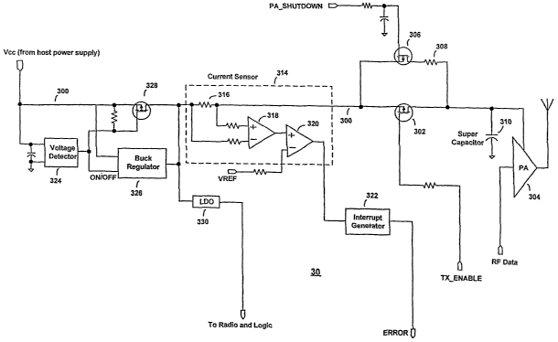
FIG. 3 shows an exemplary effective series resistance (ESR) control system,
which may be used to control the ESR of a host power supply rail of a power
supply of a
host device, according to an embodiment of the present invention;
FIG. 4 shows a graph of the current drawn by a PA of a system (e.g. wireless
network interface device) not having ESR control;
6
CA 02519932 2005-09-20
WO 2004/102820 PCT/CA2004/000733
FIG. 5 shows a graph of the current drawn by a PA of a system (e.g. wireless
network interface device) having ESR control, according to embodiments of the
present
invention; and
FIG. 6 shows a flow diagram that illustrates a method of varying and
controlling
the ESR of a power supply rail, according to embodiments of the present
invention.
DETAILED DESCRIPTION
[0011] Referring to FIG. 3, there is shown an exemplary effective series
resistance (ESR) control system 30, which may be used to control the ESR of a
host
power supply rail 300 of a power supply of a host device, according to an
embodiment of
the present invention.
[0012] According to this embodiment, when a wireless network interface device
(e.g. a wireless modem) coupled to the power supply rail 300 is transmitting
(e.g. during
burst transmit), the transmit TX ENABLE signal of the interface device is used
to turn
field effect transistor (FET) 302 OFF'. Under these circumstances, current
drawn by the
power amplifier (PA) 304 of the wireless network interface device bypasses FET
302 and
flows through the series combination of FET 306 and resistor 308. In an
exemplary
embodiment, the ESR under these circumstances is 0.83 S2. On the other hand,
when PA
304 is not transmitting, both FET 302 and FET 306 axe ON and current flows
through
both FET 302 and the series combination of FET 306 and resistor 308. Under
these
circumstances, FET 302 is in parallel with the series combination of FET 306
and resistor
7
CA 02519932 2005-09-20
WO 2004/102820 PCT/CA2004/000733
308. Consequently, the ESR of the power supply rail 300 is lower (0.17 S2 in
an
exemplary embodiment) than when the interface device is transmitting.
(0013] According to embodiments of the present invention, varying the ESR of
power supply rail 300 allows a super capacitor 310 to be controlled so that it
functions as
the primary current source (as opposed to the host power supply) for the PA
304 during
the time the wireless network interface device is transmitting data, e.g.,
during burst
transmits. It is during burst transmits that a supplemental current source,
besides the host
power supply, is needed, not only so that the massive current demands required
of the PA
304 can be provided, but also so that the maximum allowable current draw from
the host
power supply, as specified by a relevant standard, is complied with. During
burst
transmits, the ESR of the supply rail 300 is increased to a value that is
greater than the
ESR of the super capacitor. When the wireless network interface device is not
transmitting, the ESR of the power supply rail 300 is lowered to a value that
is less than
the ESR of the super capacitor 310, thereby placing the super capacitor 310 in
a charging
state. Under this condition, the super capacitor 310 is allowed to charge so
that it is able
to supply current to the PA 304 during subsequent burst transmits.
[0014] By supplementing the current drawn from the host power supply with
current from the super capacitor during transmission, the large currents
required for Class
8 and Class 10 modem burst transmits can be provided without violating the
relevant
maximum host supply current draw specification. In particular, according to an
embodiment of the present invention, the ESR control system 30 of FIG. 3 can
be used to
CA 02519932 2005-09-20
WO 2004/102820 PCT/CA2004/000733
allow Class 10 operation while still maintaining compliance with the CF+ 500
mA
maximum current draw specification. This capability is demonstrated in Table I
below.
Table I compares the peak current drawn by an RF power amplifier of a wixeless
network
interface device, under Class 10 operation, for circumstances where: {i) no
super
capacitor or ESR control present; (ii) with a super capacitor present but no
ESR control
present; and (iii) with both a super capacitor and ESR control present, the
latter
circumstance illustrative of an embodiment of the present invention.
[0015]
Without SuperWith Super CapacitorWith Super
Capacitor
Capacitor and Without and With ESR
and ESR
Without ESR Control Control
Control
Peak Current1.21 amps 0.511 amps 0.441 amps
Draw
Table I
[0016] Table I shows that when no super capacitor and no ESR control are
present, the peak current drawn by the power amplifier from a host power
supply is in
excess of 1 A. Hence, the PCMCIA maximum current draw specification of 1.0 amp
is
violated as too is the CF+ maximum current draw specification of O.S amps. The
addition of the super capacitor lowers the current draw from the host supply
down to
O.S11 amps. This brings the power amplifier into compliance with the PCMCIA
specification. However, use of the super capacitor alone is insufficient to
bring the power
amplifier into compliance with the CF+ maximum current draw specification. In
contrast
to the first two circumstances, when both a super capacitor and the ESR
control methods
9
CA 02519932 2005-09-20
WO 2004/102820 PCT/CA2004/000733
and apparatus of the present invention are employed, the peak current drawn by
the
power amplifier from the host power supply is 0.441 amps. This brings the
power
amplifier into compliance with both the PCMCIA and CF+ specifications.
[0017] During normal operation FET 306 of the ESR control system 30 is ON.
However, if an over-current condition arises as may happen, for example, if
the antenna
312 of the wireless modem is damaged, FET 306 provides over-current
protection. In
particular, once the current demand of the wireless modem exceeds some
predetermined
threshold, a PA SHUTDOWN signal (e.g. an interrupt issued by a microprocessor
on the
wireless network interface card) may be coupled to the control gate of FET 306
to turn
FET 306 OFF, and thereby decouple the host power supply from the PA 304.
[0018] Although not required, as shown in FIG. 3, the ESR control system 30
may also include a current sensor 314 that is configured to measure the
current being
drawn by the PA 304. A very low voltage dropped across low resistance resistor
316 is
used to 'measure' a voltage drop across the resistor. This measured voltage is
coupled to
inputs of a first operational amplifier (op-amp) 318, which provides a voltage
at its output
that is representative of the current being drawn by the PA 304. The output of
op-amp
318 is compared to a reference voltage, VREF, using a second op-amp 320
configured as
a comparator. If the voltage of the output of the first op-amp 318 exceeds
VREF an over-
current condition (e.g which may occur, for example if the modem antenna is
broken) has
been detected. This over-current detection can then be provide to an interrupt
generator
CA 02519932 2005-09-20
WO 2004/102820 PCT/CA2004/000733
322 to generate an ERROR signal, which can be used to notify the user or the
firmware
of the wireless modem that there is a problem.
[0019] Although not required, as shown in FIG. 3, the ESR control system 30
may also include a voltage detector 324 and a buck regulator 326 to
accommodate either
3.3 or 5 volt host supply nominal voltages. These optional components help to
maximize
power efficiency and to minimize heat dissipation. The voltage detector 324
detects
which of these two voltages power supply rail 300 is at. If at 3.3 volts
nominal, a pass
transistor 328 is turned ON, the buck regulator is bypassed, and the supply
voltage is
allowed to pass to the PA 304. On the other hand, if the supply voltage is at
5 volts
nominal, pass transistor 328 is fumed OFF and the buck regulator 326 converts
the S
volts to a 3.3 volts, which voltage is then allowed to pass to the PA 304. In
either case, a
low drop out (LDO) regulator 330 may by optionally included as a means fox
supplying
power to the rest of the wireless network interface device (e.g., not PA, but
rest of the
radio portion of the interface device, logic circuitry, etc.).
[0020] Referring now to FIGS. 4 and 5, there are shown oscilloscope (scope)
charts of a Class 10, 0.8 Watt GSM system without ESR control (FIG. 4) and
with ESR
control (FIG. 5). The scope chart for the system with ESR control (i.e. FIG.
5) employs
an ESR control system like that shown in FIG. 3. The scope chart in FIG. 4
shows the
current drawn from a host power supply by a PA of the wireless network
interface device
not having the TX ENABLE controlled FET 302 or the series combination of FET
306
and resistor 308. The scope chart in FIG. 4 shows that the current draw from
the host
11
CA 02519932 2005-09-20
WO 2004/102820 PCT/CA2004/000733
supply by the PA is about 500 mA, which is the upper limit of the CF+ maximum
allowable current draw specification. By contrast, tlxe scope chart in FIG. 5
shows, by
the absence of the peak currents during burst transmits, that the additional
current drawn
by the PA 304 during burst transmits is nearly entirely supplied by the super
capacitor
and not the host power supply.
[0021] Referring now to FIG. 6, there is shown a flow diagram illustrating a
method of varying and controlling the ESR of a power supply rail, according to
an
embodiment of the present invention. At step 602, the host power supply
voltage is
coupled to the power supply rail of the wireless network interface device. At
optional
step 604, a determination is made whether the host nominal supply voltage is
3.3 volts or
volts. If the voltage detector 324 / buck regulator 326 apparatus described
above is not
present the method continues at step 610. Otherwise, if it is determined that
the host
nominal supply voltage is 3.3 volts, the supply voltage is allowed to pass to
the PA 304
of the wireless network interface device. If it is determined that the host
nominal supply
voltage is 5 volts, the 5 volts is converted to 3.3 volts nominal by the buck.
regulator.
Next, at optional step 610, the system determines (e.g. using a current sensor
314)
whether there exists an over-current condition (i.e. current draw exceeding
some
predetermined or specified limit) measurement is performed. It should be noted
that this
step does not necessarily have to occur in the chronology shown in the flow
diagram in
FIG. 6. Indeed, it may occur at other times in the process and may even be
performed at
all times during the process. If optional step 610 is not performed, the
method continues
at decision block 612, where it is determined whether a burst transmit is
commencing. If
12
CA 02519932 2005-09-20
WO 2004/102820 PCT/CA2004/000733
yes, the ESR of the power supply rail is increased and the system transmits
with the aid
of super capacitor 310. If no, the ESR is left unchanged and the super
capacitor remains
in a charging state, unless the system has just completed a burst transmit, in
which case
the ESR is lowered to transition the super capacitor 310 into the charging
state. If at
optional step 610 an over-current condition is detected, at optional step 618
an interrupt
flag is generated, after which at step 620 the power supply rail is decoupled
from the PA
304.
(0022] Whereas the above is a complete description of the preferred
embodiments
of the invention, various alternatives, modifications, and equivalents may be
used. For
example, whereas some of the description provided above is presented in the
context of a
wireless network interface device (e.g. a wireless modem), CompactFlash cards
and
compliance with the CF+ specification, those skilled in the art will readily
understand
that the spirit of the invention encompasses not just wireless modems,
CompactFlash
cards, and compliance with the CF+ specification, but also encompasses PC Card
and PC
Card like interface devices. Indeed, the inventions disclosed in this
specification are
applicable to any host l wireless network interface device application that is
current
limited. Therefore, the above description should not be taken as limiting the
scope of the
invention as it is defined by the appended claims.
13