Note: Descriptions are shown in the official language in which they were submitted.
CA 02520250 2005-09-23
. . 1
DESCRIPTION
MICRO RELAY
TECHNICAL FIELD
The present invention relates to a micro relay manufactured by means of
semiconductor micromachining technology.
BACKGROUND ART
Japanese Non-examined Patent Publication No.5-114347 discloses a
micro relay manufactured by means of semiconductor micromachining technology.
This micro relay is an electromagnetic relay which opens or closes contacts
using
electromagnetic force of an electromagnetic device, and comprises a base
substrate having an electromagnetic device, a frame secured to the base
substrate
through a spacer, and an armature having a permanent magnet and disposed
inside the frame. In comparison with an electrostatic relay which opens or
closes
contacts using Coulomb's force, such electromagnetic relay can have large
driving
force, so such electromagnetic relay can enhance the reliability of the relay
by
increasing contact pressure.
However, in the above micro relay, because the permanent magnet is
secured to the armature, it is necessary to connect the armature and the base
substrate through the comparatively large spacer to create a space between the
armature and the base substrate. Therefore, there is a problem that the
thickness
of the relay is large.
DISCLOSURE OF THE INVENTION
In view of the above problem, the object of the present invention is to
provide a micro relay which can reduce the thickness and enhance the
reliability.
A micro relay in accordance with the present invention comprises a base
substrate, an armature block, and a cover. The base substrate has an
electromagnetic device, and has a fixed contact on one surface thereof. The
CA 02520250 2005-09-23
2
armature block includes a frame secured to the surface of the base substrate,
a
movable plate disposed inside the frame and supported rotatably by the frame,
and a movable contact base supported by the movable plate and having a
movable contact. The movable plate cooperates with a magnetic material
provided on a surface thereof to define an armature, and is driven by the
electromagnetic device to switch on/off a connection between the fixed contact
and
the movable contact. The cover is bonded to the frame. The cover creates a
space surrounded by the frame and closed between the base substrate to
accommodate the armature and the fixed contact. The feature of the present
invention resides in that the base substrate has a storage recess for
accommodating the electromagnetic device, and the storage recess is composed
of a hole extending from the one surface of the base substrate to an rear
surface
thereof and a thin storage recess lid fixed on the one surface of the base
substrate
to close the hole, and the electromagnetic device includes a yoke, a coil
wound
around the yoke to generate a flux in response to an exciting current, and a
permanent magnet secured to the yoke to generate a flux flowing through the
armature and the yoke.
For the micro relay of the present invention, it is not necessary to provide a
spacer between the armature and the base substrate because the permanent
magnet is secured to the yoke. Therefore, this micro relay can reduce the
thickness. Furthermore, because the electromagnetic device, which includes
organic material such as a coil, is put in the storage recess and the
electromagnetic device is isolated from the contacts by the storage recess
lid, the
reliability of the contacts can be improved. Furthermore, because the storage
recess is composed of the hole and the storage recess lid, the height of the
storage recess can be maximized within a limited height of the base substrate,
so
that a larger electromagnetic device can be used. Still furthermore, a
magnetic
gap between the electromagnetic device and the armature can be minimized.
Preferably, the yoke comprises a plate-shaped cross-member and a pair
of leg pieces upstanding from both ends of the cross-member, and the permanent
CA 02520250 2005-09-23
. ` ' = '
3
magnet has a height, and its opposite faces in a height direction are
magnetized to
opposite poles, and one pole face of the permanent magnet is secured to a
longitudinal center of the cross-member between the pair of leg pieces, and
the
coil is wound around the cross-member on both sides of the permanent magnet,
and top end surfaces of the leg pieces are energized to opposite poles in
response
to the exciting current to the coil. In this case, because the permanent
magnet is
disposed at the center of the cross-member and the coil is wound on both sides
of
the permanent magnet, the electromagnetic device can be constructed thinly.
Further, the armature can rotate around the permanent magnet, so that impact
resistance and vibration resistance can increase.
More preferably, the cross-member has a concave portion in which the
permanent magnet is put. By providing the concave portion, the micro relay can
be constructed more thinly. Or, a larger permanent magnet can be used within a
limited space so as to increase the reliability of the relay. Furthermore,
positioning of the permanent magnet can be done easily.
Preferably, the cross-member has convex portions for preventing the coil
from dropping. By providing the convex portion, the coil is prevented from
moving
to the leg piece and dropping from the cross-member in a manufacturing process
of the micro relay. More preferably, the convex portions are formed at four
corners on an undersurface of the cross-member. In this case, the convex
portions can be used as a mark for positioning the electromagnetic device when
the electromagnetic device is transported in an assembling process of the
micro
relay.
Preferably, an exposed surface of the yoke and a surface of the
permanent magnet are coated with resin. In this case, the yoke and the
permanent magnet are electrically isolated, and they are protected from rust.
Furthermore, a winding of the coil is protected from burrs of the edges of the
yoke
and the permanent magnet.
Preferably, the top end surfaces of the leg pieces and a top end surface of
the permanent magnet are polished to remove resin coating, and the top end
CA 02520250 2005-09-23
4
surfaces of the leg pieces and the top end surface of the permanent magnet are
in
the same plane. In this case, it is prevented that the magnetic gap between
the
electromagnetic device and the armature increases.
Preferably, a cross-section area of each of the leg pieces is formed larger
than that of the cross-member. In this case, a predetermined cross-section
area
for magnetic path can be ensured even if the edge of the leg piece is rounded
when the yoke is processed. So, a predetermined suction power can be ensured.
As for the material of the base substrate, when the base substrate is made
of glass and the storage recess lid is made of silicon, the storage recess lid
can be
processed thinly by polish or etching. Further, when the storage recess lid is
made of a silicon layer which was formed by selectively removing a silicon
substrate and an insulating layer from a SOI substrate which comprises the
silicon
substrate and the thin film silicon layer formed on the insulation layer of
the silicon
substrate, the storage recess lid can be processed not only thinly but also
precisely.
Preferably, the cover is closely bonded to the frame to create a sealed
space surrounded by the frame and closed between the base substrate and the
cover, and the base substrate has a fixed contact through-hole extending from
the
one surface of the base substrate to the rear surface thereof, a fixed contact
electrode formed on the rear surface of the base substrate, a fixed contact
conductive layer formed on an inner surface of the fixed contact through-hole
for
an electrical connection between the fixed contact and the fixed contact
electrode,
and a thin film through-hole lid provided on the one surface of the base
substrate
to close the fixed contact through-hole. In this case, a sealed micro relay
can be
constructed, so the reliability of the contacts can be improved. Further, it
is easy
to electrically connect the fixed contact to an external circuit, while
keeping the
sealed space. Further, because the through-hole lid is in the same plane with
the
storage recess lid, it is possible to form the through-hole lid and the
storage recess
lid at the same time. As a substitute for the through-hole lid, the base
substrate
may have a metal material buried in the through-hole to close the through-
hole.
In this case, electric resistance between the fixed contact and the fixed
contact
CA 02520250 2005-09-23
electrode can be reduced.
Preferably, the base substrate has, on the one surface thereof, a wiring
trace connected electrically to the fixed contact and a ground trace connected
to
ground, and the wiring trace and the ground trace run in parallel in a spaced
5 relation to each other. In this case, it is possible to set characteristic
impedance
of the wiring trace to a desired value by designing the distance between the
wiring
trace and the ground trace appropriately.
When the sealed micro relay has the ground trace, it is preferable that the
base substrate has a ground through-hole extending from the one surface of the
base substrate to the rear surface thereof, a ground electrode formed on the
rear
surface of the base substrate for earthing, a ground conductive layer formed
on an
inner surface of the ground through-hole for an electrical connection between
the
ground electrode and the ground trace, and a ground through-hole closing means
for closing the ground through-hole. In this case, it is easy to ground the
ground
trace while keeping the sealed space.
As for a contact configuration, a DPST (Double-Pole Single-Throw) micro
relay having one normally open contact and one normally closed contact can be
configured by providing two pairs of the fixed contacts at both ends in a
longitudinal direction of the base substrate and providing two movable
contacts
corresponding to the two pairs of the fixed contacts on the armature. When one
pair of the fixed contacts of the two pairs of the fixed contacts is grounded
on the
basis of this configuration, a SPST (Single-Pole Single-Throw) micro relay
having
one normally open contact or one normally closed contact can be configured. In
this case, if the two movable contacts are connected electrically to each
other
through a conductive path, high frequency characteristic (isolation
characteristic) of
the relay can be improved, because the movable contacts are grounded when the
other pair of the fixed contacts which is not grounded is opened.
Preferably, the movable plate is supported by the frame through a
supporting spring piece having elastic deformability, and the movable contact
base
is supported by the movable plate through a pressure spring piece, and the
frame,
CA 02520250 2005-09-23
6
the movable plate, the movable contact base, the supporting spring piece, and
the
pressure spring piece are formed from one semiconductor substrate. In this
case,
it is possible to miniaturize the armature and the frame easily by means of
semiconductor micromachining technology, and moreover, it is possible to
increase the life-span of a physical connection parts between the armature and
the
frame, and so on.
Preferably, the movable plate has, on a surface facing to the base
substrate, a supporting protrusion at a longitudinal center of the movable
plate, and
an apex of the supporting protrusion is in contact with the base substrate to
allow
the movable plate to make pivot motion about the apex, and the movable plate
further has, on the surface facing to the base substrate, stopper protrusions
at both
ends in a longitudinal direction, and an apex of each of the stopper
protrusions
comes in contact with the base substrate to regulate the pivot motion of the
movable plate when the movable plate makes pivot motion. By providing the
supporting protrusion, the movable plate can make the pivot motion easily.
And,
by providing the stopper protrusions, a stroke of the armature can be
controlled
precisely.
Preferably, the apex of the supporting protrusion and the apex of each of
the stopper protrusions are in a same plane. In this case, the supporting
protrusion
and the stopper protrusions can be formed at the same time under the same
conditions. The supporting protrusion, the stopper protrusions, and the
movable
contact base may be formed so that their apexes are in a same plane. In this
case, it becomes easier to process them.
Preferably, a distance from the supporting protrusion to the movable
contact base is longer than a distance from the supporting protrusion to a
portion
of the armature which is attracted to the electromagnetic device. In this
case, it is
possible to ensure a large stroke of the movable contact, so it is possible to
ensure
enough contact pressure of the movable contact.
Preferably, a distance from the supporting protrusion to the movable
contact base is longer than a distance from the supporting protrusion to each
of the
CA 02520250 2009-04-28
7
stopper protrusions. In this case, it is possible to regulate the rotation of
the
armature by the stopper protrusion after the movable contact came in contact
with
the fixed contact.
Preferably, the pressure spring piece has a meandering part which
meanders. By providing the meandering part, the length of the pressure spring
piece is lengthened, so that the pressure which acts on the pressure spring
piece
is eased.
Preferably, the movable plate is made of a semiconductor substrate and
has a hole extending from an upper surface to a undersurface, and the magnetic
material is disposed on a surface of the movable plate so that it closes one
end of
the hole, and the armature block further has a second magnetic material ora
metal
piece, and the second magnetic material or the metal piece is disposed so that
it
closes an other end of the hole, and the magnetic material and the second
magnetic material or the metal piece are jointed to each other inside the hole
by
iaser welding, and the movable plate is sandwiched between the magnetic
material and the second magnetic material or the metal piece. In this case,
warpage and so on of the movable plate caused by difference of thermal
expansion coefficient between the movable plate and the magnetic material can
be
suppressed.
According to an aspect of the present invention there is provided a micro
relay comprising:
a base substrate having an electromagnetic device, said base substrate having
a fixed contact on one surface thereof;
an armature block including a frame secured to the surface of said base
substrate, a movable plate disposed inside said frame and supported rotatably
by said frame, and a movable contact base supported by said movable plate and
having a movable contact, said movable plate cooperating with a magnetic
material provided on a surface of said movable plate to define an armature and
being driven by said electromagnetic device to switch on/off a connection
3o between said fixed contact and said movable contact; and
a cover bonded to said frame, said convert creating a space surrounded by said
frame and closed between said base substrate and the cover to accommodate
said armature and said fixed contact,
CA 02520250 2009-04-28
7a
wherein said base substrate has a storage recess for accommodating said
electromagnetic device, said storage recess comprising a hole extending from
the one surface of said base substrate to a rear surface thereof and a thin
storage recess lid fixed on the one surface of said base substrate to close
said
hole,
wherein said base substrate has, on the one surface thereof, a wiring trace
connected electrically to said fixed contact and a ground trace connected to
ground, said wiring trace and said ground trace running in parallel in spaced
relation to each other, and
wherein said electromagnetic device comprises a yoke, a coil wound around
said yoke to generate a first flux in response to an exciting current, and a
permanent magnet secured to said yoke to generate a second flux flowing
through said armature and said yoke.
BRIEF DESCRIPTION OF THE DRAWINGS
FIG. 1 is an exploded perspective view of a micro relay in accordance with a
first
embodiment of the present invention.
FIG. 2 is a perspective view of the micro relay looked from a bottom side.
FIG. 3 is an exploded perspective view of a body of the micro relay.
FIG. 4 is a sectional view of the micro relay.
FIG. 5 is a perspective view of a yoke used in the micro relay.
FIG. 6 is a front view of an electromagnetic device of the micro relay.
FIG. 7 is a partly enlarged illustration of another configuration of the micro
relay.
FIG. 8 is a partly enlarged illustration of another configuration of the micro
relay.
CA 02520250 2005-09-23
8
FIG. 9A is a plan view of an armature block of the micro relay.
FIG. 9B is a bottom view of the armature block of the micro relay.
FIG. 10 is an exploded perspective view of the armature block of the micro
relay.
FIG. 11 is a perspective view of a cover of the micro relay looked from a
bottom
side.
FIG. 12 is a view showing another configuration of the yoke of the micro
relay.
FIG. 13 is a view showing another configuration of the electromagnetic device
of
the micro relay.
FIG. 14A is a view showing another configuration of a meandering part of the
micro relay.
FIG. 14B is a view showing another configuration of the meandering part of the
micro relay.
FIG. 14C is a view showing another configuration of the meandering part of the
micro relay.
FIG. 14D is a view showing another configuration of the meandering part of the
micro relay.
FIG. 14E is a view showing another configuration of the meandering part of the
micro relay.
FIG. 14F is a view showing another configuration of the meandering part of the
micro relay.
FIG. 15A is a view showing another configuration of a pressure spring piece of
the
micro relay.
FIG. 15B is a view showing another configuration of the pressure spring piece
of
the micro relay.
FIG. 16 is a view showing another configuration of a supporting protrusion of
the
micro relay.
FIG. 17 is a view showing another configuration of a stopper protrusion of the
micro relay.
FIG. 18 is a view showing another configuration of a cover of the micro relay.
FIG. 19A is a partly enlarged illustration of another configuration of the
micro relay.
CA 02520250 2005-09-23
9
FIG. 19B is a partly enlarged illustration of another configuration of the
micro relay.
FIG. 20A is a partly enlarged illustration of another configuration of the
micro relay.
FIG. 20B is a partly enlarged illustration of another configuration of the
micro relay.
FIG. 21 is an exploded perspective view of a micro relay in accordance with a
second embodiment of the present invention.
FIG. 22 is a view showing an armature block of the micro relay with a magnetic
material removed, looked from a bottom side.
BEST MODE FOR CARRYING OUT THE INVENTION
Hereinafter, the present invention will be described in more detail with
reference to the accompanying drawings.
(First embodiment)
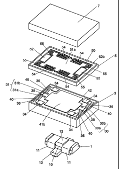
FIG. 1 shows a micro relay in accordance with a first embodiment of the
present invention. The micro relay comprises an electromagnetic device 1, a
base substrate 3, an armature block 5, and a cover 7. As shown in FIG. 2, the
base substrate 3 has, on the bottom side, a storage recess 41 for
accommodating
the electromagnetic device 1, and as shown in FIG. 3, the base substrate 3 has
two pairs of fixed contacts 30, 31, on an upper surface thereof. The armature
block 5 comprises a frame 50 secured to the upper surface of the base
substrate,
a movable plate 51 a disposed inside the frame 50 and supported rotatably by
the
frame 50 through supporting spring pieces 54, and movable contact bases 52
having movable contacts 53 on an undersurface thereof and supported by the
movable plate 51 a through pressure spring pieces 55. As shown in FIG. 4, the
movable plate 51 a cooperates with a magnetic material 51 b provided on an
undersurface thereof to define an armature 51, and is driven by the
electromagnetic device 1 to switch on/off a connection between the movable
contacts 53 and the pairs of the fixed contacts 30, 31. The cover 7 is closely
bonded to an upper surface of the frame 5. That is, the micro relay of this
embodiment is a sealed micro relay in which the armature 51, the movable
contacts 53, and the pairs of the fixed contacts 30, 31 are housed in a sealed
CA 02520250 2005-09-23
space surrounded by the frame 51 and closed between the base substrate 3 and
the cover 7.
The electromagnetic device 1 comprises a yoke 10, a coil 11 which is
wound around the yoke 10 and generates a flux in response to an exciting
current,
5 and a permanent magnet 12 which is bonded to the yoke 10 and generates a
flux
flowing through the armature 51 and the yoke 10. In more detail, as shown in
FIG.
5, the yoke 10 has a generally U-shaped configuration, and it comprises a
plate-
shaped cross-member 10a around which the coil 11 is wound and a pair of leg
pieces 10b upstanding from both ends of the cross-member 10a. The yoke 10 is
10 made of an iron plate, such as a soft magnetic iron sheet, by means of, for
example, bending process, forging process, or stamping process. The cross
section of each of the leg pieces 10b is a rectangle. The cross-member 10a has
a concave portion 10c for putting the permanent magnet 12 in, at the
longitudinal
center. The permanent magnet is a rectangular parallelepiped having a height,
and its opposite faces in the height direction are magnetized to opposite
poles, and
as shown in FIG. 6, one pole face 12b is bonded to the concave portion 10c. By
providing the concave portion 10c, the height of the electromagnetic device 1
can
be lowered. Or, a large permanent magnet which has extra height equal to the
depth of the recess 10c can be used to increase the suction power. The coil 11
is
directly wound around the cross-member 10a on both sides of the permanent
magnet 12 so that top end surfaces of the leg pieces 10b are energized to the
opposite poles in response to the exciting currents to the coil 11. When the
coil
11 is wound, the leg pieces 10b as well as the side faces of the permanent
magnet
12 act as flanges of a coil bobbin. The cross-member 10a has convex portions
10d at both ends of each of the both longitudinal side faces of the cross-
member
10a to prevent the coil 11 from dropping from the yoke 10. That is, the convex
portions 10d can prevent the coil 11 from dropping from the yoke 10 and can
prevent product failure when the micro relay is manufactured.
The yoke 10 and the permanent magnet 12 are coated with resin, such as
a polyimide, a fluorine resin, a polyamide-imide resin, a poly-para-xylylene,
and a
CA 02520250 2005-09-23
11
mixture thereof, after the permanent magnet 12 is bonded to the yoke 10. The
coating can isolate the yoke 10 and the permanent magnet 12. The coating can
also protect the yoke 10 and the permanent magnet 12 from rust. Furthermore,
the coating can prevent a winding of the coil from being broken by burrs of
the
yoke and the permanent magnet 12 when the coil is wound, because the coating
covers the burrs on the surfaces of the yoke and the permanent magnet 12. In
order to prevent the winding of the coil from being broken, the edges of the
yoke
and the four corners of the top end surface of the permanent magnet 12 may be
rounded. For rounding the edges of the yoke 10, chemical etching can be used.
Furthermore, the top end surfaces of the leg pieces 10b and a pole face
12a of the permanent magnet 12 are polished at the same time, and these three
surfaces, namely the top end surfaces of the leg pieces 10b and the pole face
12a
of the permanent magnet, are in the same plane. As a result, it is prevented
that
the magnetic gap between the electromagnetic device 1 and the armature 51
increases, so that the magnetic gap is stabilized and the suction power is
stabilized.
As shown in FIG. 6, a thickness (t2) of each of the leg pieces 10b is
formed thicker than a thickness (t1) of the cross-member 10a so that a cross-
section area of each of the leg pieces 10b becomes larger than that of the
cross-
member 10a. As a result, a predetermined cross-section area for the magnetic
path can be ensured even if the edge of the leg piece is rounded when the yoke
is
processed, so a predetermined suction power can be ensured without saturation
of
the magnetic flux.
As shown in FIG. 2, a coil terminal block 13 is secured to the center of the
undersurface of the cross-member 10a along a direction perpendicular to the
longitudinal direction of the cross-member 10a. The coil terminal block 13 has
conductive traces 13a at both ends of the undersurface and each end of the
coil 11
is electrically connected to each of the conductive traces 13a. Further, a
first
bump (a coil electrode) 13b is bonded to each of the conductive traces 13a for
an
electrical connection between the electric circuit on the printed board for
carrying
the micro relay and the coils. Instead of the bump 13b, an electrode pad for
CA 02520250 2005-09-23
. . . .
12
bonding wire may be formed.
The base substrate 3 is made of heat resistance glass, such as Pyrex (R),
and is formed into a rectangular shape. As shown in FIG.3, the pair of the
fixed
contacts 30 is composed of fixed contacts 30a and 30b which are disposed in a
spaced relation to each other, and the pair of the fixed contacts 30 is
disposed on
the upper surface of the base substrate 3 at longitudinal one end of the base
substrate 3. The pair of the fixed contacts 31 is composed of fixed contacts
31 a
and 31 b which are disposed in a spaced relation to each other, and is
disposed on
the upper surface of the base substrate 3 at the other longitudinal end of the
base
substrate. The base substrate 3 has, near its four corners, fixed contact
through-
holes 32 extending from the upper surface of the base substrate 3 to the
undersurface thereof. On a periphery of each end of each of the through-holes
32, a land 33 is formed. Each of the fixed contacts is electrically connected
to an
adjacent land 33 on the upper surface of the base substrate 3 through a linear
wiring trace 36 formed on the upper surface of the base substrate 3. The lands
33 at both ends of each of the through-holes 32 are electrically connected to
each
other through a fixed contact conductive layer formed on the inner surface of
each
of the through-holes 32 from a conductive material. The opening of each
through-
hole 32 is in the form of a circle, and the opening of each of the through-
hole on
the upper surface side of the base substrate 3 is closed by a first lid (a
through-
hole lid) 34 formed from a silicon thin film. A second bump 35 is secured to
each
of the lands 33 on the undersurface side of the base substrate 3, as a fixed
contact
electrode. After all, each of the fixed contacts is electrically connected to
each of
the second bump (the fixed contact electrode) 35 through the wiring trace 36
and
the fixed contact conductive layer.
Furthermore, the base substrate 3 has, at both ends in the longitudinal
direction, ground through-holes 37 extending from the upper surface of the
base
substrate 3 to the undersurface thereof. The land 33 is also formed on a
periphery of each end of each of the ground through-holes 37, and the lands 33
of
both ends of each of the ground through-holes 37 are electrically connected to
CA 02520250 2005-09-23
13
each other by a ground conductive layer (not shown) formed on the inner
surface
of each of the ground through-holes 37. The opening of each ground through-
hole 37 is in the form of a circle, and the opening of each of the ground
through-
holes 37 on the upper surface side of the base substrate 3 is closed by a
second
lid (a ground through-hole lid) 38 formed from a silicon thin film. A third
bump 39
is fixed to each of the lands 33 on the undersurface side of the base
substrate 3,
as a ground electrode. Each of the ground through-holes 37 is located at the
center of the base substrate 3 in a direction perpendicular to the
longitudinal
direction, and, on both sides of the ground through hole in the direction
perpendicular to the longitudinal direction of the base substrate 3, ground
traces 40
are formed on the upper surface of the base substrate 3. Each of the ground
traces 40 is electrically connected to the land 33 of the ground through-hole
37 and
each of the ground traces 40 is connected to the third bump (the ground
electrode)
39 through the ground conductive layer. The ground trace 40 has a linear
configuration, and runs parallel to the wiring trace 36 at fixed intervals
(t3). The
characteristic impedance of the wiring trace 36 can be set to a desired value
by
changing the intervals (t3) appropriately to improve the high frequency
characteristic of the micro relay.
The fixed contacts and the wiring traces 36 and the ground traces 40 and
the lands 33 can be made of a conductive material, for example, Cr, Ti, Pt,
Co, Cu,
Ni, Au, or an alloy thereof. The first bumps 13b, the second bumps 35, and the
third bumps 39 can be made of a conductive material such as Au, Ag, Cu, and
soldering. Each of the through-holes 32, 37 can be formed by sandblasting,
etching, drilling, supersonic machining, and so on. The conductive layer of
each
of the through-holes is made of a conductive material such as Cu, Cr, Ti, Pt,
Co, Ni,
Au, or an alloy thereof, and is formed by means of plating, deposition,
sputtering,
and so on.
Instead of closing the through-holes by using the first lids (the through-hole
lids) 34 and the second lids (the ground through-hole closing means) 38, each
of
the through-holes may be closed by burying a metal material 43 in the through-
CA 02520250 2005-09-23
14
hole, as shown in FIG. 7. The metal material 43 can be formed by plating. In
this case, airtightness of the sealed space can be improved. If a material
having
high electric conductivity, such as Cu, Ag, and soldering, is used as a
material of
the plating, electric resistance between the fixed contact and the second bump
(the
fixed contact electrode) 35 or between the ground trace 40 and the third bump
(the
ground electrode) 39 can be reduced. As shown in FIG. 8, a constricted part 44
may be formed inside the through-hole, and the metal material 43 may be buried
only near the constricted part 44. In this case, it becomes easy to plate the
through-hole. Also, the amount of the metal material 43 can be reduced.
As mentioned above, the base has the storage recess 41 for
accommodating the electromagnetic device 1 at the center on the bottom side of
the base substrate 3. As shown in FIG. 3, the storage recess 41 is composed of
a hole 41 a extending from the upper surface of the base substrate 3 to the
undersurface thereof, and a third lid (a storage recess lid) 41 b made of a
silicon
thin film and fixed on the upper surface of the base substrate 3 to close the
hole
41 a. The opening of the hole 41 a is in the form of a cross, and the hole 41
is
formed in a tapered shape in which the opening area of the hole 41 a becomes
larger gradually toward the undersurface side of the base substrate 3 in order
to
reduce the opening area of the hole 41 on the upper surface side of the base
substrate 3 and in order to make it easy to insert the electromagnetic device
into
the hole 41 from the undersurface side of the base substrate 3. The
electromagnetic device 1 is housed in the storage recess 41 with the top end
surfaces of the leg pieces 10b upward. As shown in FIG. 6, positioning hollows
41 c are formed in the undersurface of the third lid (the storage recess lid)
41 b, and
the electromagnetic mechanism 1 is disposed in the storage recess 41 with the
top
end surfaces of the leg pieces 10b and the pole face 12a of the permanent
magnet
12 fitted into the positioning hollows 41 c in order to dispose the
electromagnetic
device 1 in the storage recess 41 with precision. When the electromagnetic
device 1 was housed in the storage recess 41, the electromagnetic device 1 is
isolated from the pairs of the fixed contacts 30 and 31 and the movable
contacts
CA 02520250 2005-09-23
53 by the third lid (the storage recess lid) 41 b. That is, the
electromagnetic device
1 which includes organic material such as a coil is isolated from the contacts
by the
third lid (the storage recess lid) 41 b. Therefore, the reliability of the
contacts can
be improved. Furthermore, because the storage recess 41 is composed of the
5 hole 41 a and the third lid (the storage recess lid) 41 b, the height of the
storage
recess 41 can be maximized within a limited height of the base substrate 3.
Therefore, a larger electromagnetic device can be used. Still furthermore,
because the third lid (the storage recess lid) 41 b is made of a silicon thin
film, a
magnetic gap between the electromagnetic device and the armature can be
10 minimized.
After the electromagnetic device 1 is housed in the storage recess 41,
interstices in the storage recess 41 are filled with potting compound, as
shown in
FIG. 4, to fix the electromagnetic device 1 to the base substrate 3. As the
potting
compound, silicon resin which has elastic deformability even after it hardened
is
15 preferable. The height of the electromagnetic device 1 is designed so that
the
undersurface of the coil terminal block 13 is in the same plane with the
undersurface of the base substrate 3 when the electromagnetic device 1 was
housed in the storage recess 41.
The first lid 34, the second lid 38, and the third lid 41 b are formed by
processing a silicone substrate thinly by means of polish, etching, etc., and
the
thickness of each lid is set to 20,um. The thickness of each lid is not
limited to 20
um, but it can be set appropriately between about 5 pm and about 50 pm.
Alternatively, the first lid 34, the second lid 38, and the third lid 41 b may
be made
of a silicon layer which was formed by selectively removing a silicon
substrate and
an insulating layer from a SOI substrate which was composed of the silicon
substrate and the thin film silicon layer formed on the insulation layer of
the silicon
substrate. In this case, each of the lids can be processed not only thinly but
also
precisely. Alternatively, a glass thin film formed by processing a glass
substrate
thinly by polish, etching, etc., may be used for the lids.
The armature block 5 except for the magnetic material 51 b (namely, the
CA 02520250 2005-09-23
16
frame 50, the movable plate 51 a, the movable contact bases 52, the supporting
spring pieces 54, and the pressure spring pieces 55) is formed by processing
one
semiconductor substrate by means of semiconductor micromachining technology.
As the semiconductor substrate, a silicon substrate having about 50 /im to
about
300 pm, preferably 200Mm, in thickness is preferable. As shown in FIGS. 9A,
9B,
and 10, the frame 50 of the armature block 5 is a rectangular frame having
about
the same circumference as the base substrate 3. The movable plate 51 a is in
the
form of a flat plate, and it has first projecting pieces 56 at the center of
each of the
longitudinal sides of the movable plate 51 a and second projecting pieces 57
at four
corners thereof. Each of the first projecting pieces 56 has, on the base
substrate
3 side, a supporting protrusion 58 which is in the form of a frustum of a
quadrangular pyramid, and each of the second projecting pieces 57 has, on the
base substrate 3 side, a stopper protrusion 59 which is in the form of a
frustum of a
quadrangular pyramid. The supporting protrusions 58 and the stopper
protrusions 59 are processed so that the apexes of the supporting protrusions
58
and the apexes of the stopper protrusions 59 are in the same plane. After the
armature block 5 is bonded to the base substrate 3, the apex of each of the
supporting protrusions 58 is always in contact with the upper surface of the
third lid
(the storage recess lid) 41 b and defines a fulcrum of the armature 51. The
supporting protrusions 58 allow the armature to make pivot motion stably. The
apex of each of the stopper protrusions 59 comes in contact with the upper
surface
of the base substrate 3 (not the upper surface of the third lid 41 b) when the
armature 51 makes the pivot motion, and it regulates the pivot motion of the
armature 51. Therefore, a stroke of the armature 51 can be controlled
precisely
by controlling the dimensions of parts of the supporting protrusions 58 and
the
stopper protrusions 59 projecting from the movable plate 51. Because the
armature block 5 is manufactured by means of the semiconductor micromachining
technology, the control of the dimensions of the parts of the supporting
protrusions
58 and the stopper protrusions 59 is easy even 'rf the micro relay is small.
In
addition, because the apexes of the supporting protrusions 58 and the stopper
CA 02520250 2005-09-23
17
protrusions 59 are in the same plane, the supporting protrusions 58 and the
stopper protrusions 59 can be formed at the same time under the same
conditions.
So, it is easy to manufacture the micro relay. The shape of the stopper
protrusion
58 and the shape of the stopper protrusion 59 are not limited to the frustum
of a
quadrangular pyramid, but it may be, for example, in the form of a
quadrangular
prism.
Each of the first projecting pieces 56 has a convex part 56a on the side
face facing to the frame 50, and the frame 50 has, on the inner surface of the
frame 50 facing to the convex parts 56a, third projecting pieces 60 each of
which
has a concave part 60a. Each of the convex parts 56a is engaged into the
corresponding concave part 60a in the same plane as the frame 50, and the
convex part 56a and the concave part 60a define a movement restriction part 61
which restricts a horizontal movement of the armature 51. Because there is a
clearance between the convex part 56a and the concave part 56a, the movement
restriction part 61 does not interfere with the pivot motion of the armature
51.
The magnetic material 51 b is fixed on a surface of the movable plate 51 b
on the base substrate 3 side to define the armature 51 together with the
movable
plate 51 a. The magnetic material 51 b is made of, for example, soft magnetic
iron,
magnetic stainless, Permalloy, 42 alloy, etc. by means of machining process,
etching, plating, and so on. The magnetic material 51 is designed to be
thinner
than the frame in thickness in order to create a predetermined gap between the
magnetic material 51 b and the third lid (the storage recess lid) 41 b when
the
armature block 5 was bonded to the base substrate 3.
The movable plate 51 a is rotatably supported by the frame 50 through
supporting spring pieces 54 having elastic deformability. The supporting
spring
pieces 54 are formed at two sites on each longitudinal side of the movable
plate 51
in a spaced relation to each other. One end of each of the supporting spring
pieces 54 is connected to the frame 50 integrally, and the other end of it is
connected to the movable plate 51 a integrally. The supporting spring pieces
54
give the armature 51 return force when the armature 51 rotates. Each of the
CA 02520250 2005-09-23
18
supporting spring pieces 54 has, between the one end thereof and the other end
thereof, a meandering part 54a which meanders in one plane. By providing the
meandering part 54, the supporting spring pieces 54 is lengthened, whereby the
pressure which acts on the supporting spring pieces 54 when the movable plate
51 a rotates can be distributed. Therefore, the meandering part 54a can
prevent
the supporting spring pieces 54 from being destroyed.
The movable contact base 52 is disposed between the armature 51 and
the frame 50 at both longitudinal ends of the armature 51. The undersurface of
each of the movable contact bases 52 projects below the undersurface of the
armature 51. The movable contact 53 made of conductive material is fixed on
the
undersurface of each of the movable contact bases 52. Preferably, for easy
manufacturing, the movable contact bases 52 are processed so that the apex of
each of the movable contact bases 52 is in the same plane as the apex of each
of
the supporting protrusions 58 and the apex of each of the stopper protrusions
59.
Each of the movable contact bases 52 is supported by the movable plate 51 a
through two pressure spring pieces 55 which have elastic deformability and
give
the contact pressure to the movable contact 53. Each of the pressure spring
pieces 55 is formed so that it detours around the second projecting pieces 57,
and
one end of the each of the pressure spring pieces 55 is connected to the side
of
the movable contact base 52 integrally and the other end of it is connected to
the
side of the movable plate 51 a integrally. Each of the pressure spring pieces
55
has a meandering part 55a in the middle part thereof. By providing the
meandering part 55a, each of the pressure spring pieces 55 is lengthened, so
that
the pressure which acts on the pressure spring pieces 55 when the movable
plate
51 a rotates can be distributed. Therefore, the spring constant of the
pressure
spring piece 55 can be reduced without changing the cross-section area of the
pressure spring piece 55 perpendicular to the running direction of the
pressure
spring piece 55. Or, the strength of the pressure spring pieces 55 can be
improved without changing the spring constant by increasing the cross-section
area of the pressure spring pieces 55. The distance between one movable
CA 02520250 2005-09-23
19
contact 53 and the corresponding fixed contacts at the time when the movable
contact 53 separates from the fixed contacts can be set to an intended
distance by
changing the thickness of the movable contact base 52 and/or the thickness of
the
movable contact 53.
In this embodiment, because each of the movable contact bases 52 is
disposed between the longitudinal end of the armature 51 and the frame 50, a
distance from one supporting protrusion 58 to one movable contact base 52 is
longer than a distance from the supporting protrusion 58 to a portion of the
magnetic material 51 b which is attracted to the electromagnetic device 1
(that is, a
portion of the magnetic material 51 b facing to the leg piece 10b of the yoke
10).
Therefore, the stroke of the movable contact base 52 is larger than that of
the
armature 51 when the armature 51 rotates in response to the suction power of
the
electromagnetic device 1. Therefore, it is possible to ensure a large stroke
of the
movable contact 53 even if the micro relay is small, so it is possible to
ensure
enough contact pressure of the movable contact.
Also, because each of the stopper protrusions 59 is located between the
supporting protrusion 58 and the movable contact base 52, a distance from one
supporting protrusion 58 to one movable contact base 52 is longer than a
distance
from the supporting protrusion 58 to one stopper protrusion 59. Therefore,
when
the armature 51 rotates, it is possible to regulate the rotation of the
armature by the
stopper protrusions 59 after the movable contact 53 came in contact with the
fixed
contact and obtained enough contact pressure.
The cover 7 is made of heat resistance glass, such as Pyrex (R), and, as
shown in FIG. 11, it has, in a surface on the armature block side, a recess 70
for
creating a space for the pivot motion of the armature 51. The cover 7 has
about
the same circumference as the frame 50 and the base substrate 3, and the cover
7,
the frame 50, and the base substrate 3 forms one rectangular parallelepiped,
when
they were bonded to each other.
In order to bond the base substrate 3 and the frame 50 to each other, a
metal thin film 42 for bonding is formed over entire circumference of a
periphery of
CA 02520250 2005-09-23
the upper surface of the base substrate 3, and a metal thin film 62a for
bonding is
formed over entire circumference of a periphery of the undersurface of the
frame
50. Also, in order to bond the frame 50 and the cover 7 to each other, a metal
thin film 62a for bonding is formed over entire circumference of a periphery
of the
5 upper surface of the frame 50, and a metal thin film 71 for bonding is
formed over
entire circumference of a periphery of the undersurface of the cover 7. The
base
substrate 3 and the armature block 5 are closely bonded to each other by
pressure
bonding between the metal thin film 42 and the metal thin film 62a, and the
armature block 5 and the cover 7 are closely bonded to each other by pressure
10 bonding between the metal thin film 62b and the metal thin film 71. Because
the
hole 41 a of the storage recess 41, the fixed contact through-holes 32, and
the
ground through-holes 37 are closed by the lid 41 b, the lid 34, and the lid
38,
respectively, a sealed space surrounded by the frame 50 and closed between the
base substrate 3 and the cover 7 is created, and the armature 51, the pairs of
the
15 fixed contacts 30, 31, and the movable contacts 53 are housed inside the
sealed
space. Therefore, it is prevented that external foreign body gets inside the
micro
relay and degrades the reliability of the contact. In order to prevent the
surface of
the fixed contacts and the movable contacts 53 from being oxidized and
degraded,
the sealed space may be evacuated, or inert gases may be encapsulated. These
20 metal thin films 42, 62a, 62b, and 71 can be made of, for example, Au, Al-
Si, Al-Cu,
and so on.
When the micro relay constituted as above is mounted on a printed circuit
board, first, the first bumps 13b, the second bumps 35, and the third bumps 39
are
formed on the undersurface of the base substrate 3 by means of soldering
balls,
as shown in FIG. 2. Then, the first bumps (the coil electrodes) 13b are
connected
to driving conductive traces formed on the printed circuit board, and the
second
bumps (the fixed contact electrodes) 35 are connected to signal conductive
traces
formed on the printed circuit board, and the third bumps (the ground
electrodes) 39
are connected to ground conductive traces formed on the printed circuit board.
Or, the micro relay may fixed on the printed circuit board in a reversed state
(that is,
CA 02520250 2005-09-23
21
a state shown in FIG.2), and these bumps 13b, 35, 39 may be bonded to the
printed circuit board by means of wire bonding.
Hereinafter, the movement of the micro relay will be described. When
the coil 11 was energized, a flux generated by the coil 11 flows in the same
direction as a flux of the permanent magnet 12 at one leg piece 10b of the
yoke 10
and it flows in the direction opposite to the flux of the permanent magnet 12
at the
other leg piece 10b. Therefore, suction power is generated between the top end
surface of the one leg piece 10b and the magnetic material 51 b, so that one
longitudinal end of the magnetic material 51 b is attracted to the top end
surface of
the one leg piece 10b, and the armature 51 begins to rotate about the two
supporting protrusions 58. And that time, the movable contact bases 52 begins
to
rotate together with the armature 51, and the movable contact 53 fixed on one
movable contact base 52 comes in contact with the corresponding pair of the
fixed
contacts 30 (or 31) so as to electrically connect the fixed contact 30a (or 31
a) and
the fixed contact 30b (or 31 b).
At a point in time when the movable contact 53 came in contact with the
pair of the fixed contacts 30 (or 31), the apexes of the stopper protrusions
59 do
not come in contact with the base substrate 3, and the armature 51 rotates
further
(in other words, the armature 51 over-travels. ). The pressure spring pieces
55
are bent by this over-travel, and, contact pressure in accordance with an
amount of
the over-travel of the armature 51 (in other words, a travel amount of the
armature
51 after the movable contact 53 came in contact with the pair of the fixed
contacts
(or 31)) is generated between the movable contact 53 and the pair of the fixed
contacts 30 (or 31). After that, the apexes of the stopper protrusions 59 come
in
25 contact with the base substrate 3 to regulate the rotation of the armature
51.
Even if the energization of the coil 11 is stopped in this condition, the
connection
between the movable contact 53 and the pair of the fixed contacts 30 (or 31)
is
maintained by the flux generated by the permanent magnet 12.
When the coil 11 is energized in the opposite direction, the magnetic
30 material 51 b is attracted to the other leg piece 1 0b of the yoke 10, and
the
CA 02520250 2005-09-23
22
armature 51 begins to rotate, and the movable contact 53 fixed on the other
movable contact base 52 comes in contact with the corresponding pair of the
fixed
contacts 31 (or 30). And, contact pressure is generated by the over-travel of
the
armature 51, and then the rotation of the armature 51 is regulated by the
stopper
protrusions 33a. Even if the energization of the coil 11 is stopped in this
condition,
the connection between the movable contact 53 and the pair of the fixed
contacts
31 (or 30) is maintained by the flux generated by the permanent magnet 12.
As mentioned above, it is not necessary for the micro relay of this
embodiment to provide a spacer between the armature and the base substrate
because the permanent magnet 12 is secured to the yoke 10, therefore, the
micro
relay can reduce the thickness. The thickness of the entire micro relay is
defined
by a total of the thickness of the base substrate 3, the thickness of the
frame 50,
and the thickness of the cover 7. Furthermore, because the electromagnetic
device 1 is housed in the storage recess 41 and is isolated from the contacts
by
the third lid (the storage recess lid) 41 b, the micro relay has high
reliability.
Although the base substrate 3 and the cover 7 are made of glass
substrate respectively in this embodiment, one of the base substrate 3 and the
cover 7, or both of the base substrate 3 and the cover 7, may be made of
silicon
substrate. If the base substrate 3 and the cover 7 are made of glass substrate
respectively and the armature block 5 is made of silicon substrate, the base
substrate 3 and the armature block 5, as well as the armature clock 5 and the
cover 7, can be bonded directly by means of anodic bonding. In this case, the
metal thin films for bonding 42, 62a, 62b, 71 can be eliminated.
As to the electromagnetic device 1, although the convex portions 10d for
preventing the drop of the coil 11 are formed at both ends of each of the
longitudinal side faces of the cross-member 10a in this embodiment, the convex
portions 10d may be formed at four corners on the undersurface of the cross-
member 10a, as shown in FIG. 12. In this case, the convex portions 10d can not
only work to prevent the coil 11 from dropping, but also work to decide the
position
of the electromagnetic device when the electromagnetic device is transported
in a
CA 02520250 2005-09-23
23
process of assembling the micro relay or when the electromagnetic device is
transferred by a parts feeder. As shown in FIG. 13, notches 14 may be formed
at
both longitudinal ends of the coil terminal block 13 to wind the ends of the
coil 11
easily around the coil terminal block 13.
As to the armature block 5, the meandering part 54a of the supporting
spring piece 54 and the meandering part 55a of the pressure spring piece 55
may
have a shape shown in FIGS. 14A to 14F. As shown in FIG. 15A, one end of the
pressure spring piece 55 may be integrally connected to the second projecting
piece 57. Or, as shown in FIG. 15B, the pressure spring piece 55 may be
disposed beside the longitudinal side surface of the movable plate 51 a. As
shown in FIG. 16, the supporting protrusions 58 may be formed on the upper
surface of the third lid (the storage recess lid) 41 b, instead of being
formed on the
first projecting pieces 56. Also, as shown in FIG. 17, the stopper protrusions
59
may be formed on the upper surface of the third lid (the storage recess lid)
41 b,
instead of being formed on the second projecting pieces 57. Although, in this
embodiment, the spring constant of the supporting spring piece 54 was decided
so
that the suction power by the permanent magnet 12 is larger than the return
power
of the supporting spring piece 54, the spring constant of the supporting
spring
piece 54 may be decided so that the suction power by the permanent magnet 12
is
smaller than return power of the supporting spring piece 54.
As to the cover 7, as shown in FIG. 18, it is preferable that a metal thin
film
71 is secured to the upper surface of the cover, and the metal thin film 71 is
marked with a lot number, a brand name, etc. by means of a laser marking
device.
In this case, even if the micro relay is small, visibility of the lot number,
a brand
name, etc. can be improved.
Hereinafter, manufacturing method of the micro relay of this embodiment
will be described briefly. The manufacturing method includes an armature block
forming process, a sealing process, and an electromagnetic device setting
process.
In the armature block forming process, a silicon substrate is processed by
means
of semiconductor micromachining technology, namely micro machining technology,
CA 02520250 2005-09-23
24
such as lithography technology, and etching technology so as to form the frame
50,
the movable plate 51 a, the movable contact bases 52, the supporting spring
pieces 54, and the pressure spring pieces 55. Then, the magnetic material 51 b
is
secured to the surface of the movable plate 51 a on the base substrate 3 side,
and
the movable contact 53 is bonded to the movable contact base 52. In the
sealing
process, the armature block 5, the base substrate 3, and the cover 7 are
bonded to
each other by means of pressure bonding or anodic bonding so as to create a
sealed space surrounded by the base substrate 3, the cover 7, and the frame 50
of
the armature block 5. In the electromagnetic device setting process, the
electromagnetic device 1 is housed in the storage recess 41 of the base
substrate
3, and then the electromagnetic device 1 is fixed to the base substrate 3.
To form the base substrate 3, first, the hole 41 a of the storage recess 41
and the through-holes 32 and 37 are formed in a glass substrate which becomes
a
basis for the base substrate 3 by etching, or sandblasting, and then the lands
33,
the pairs of the fixed contacts 30 and 31, the wiring traces 36, the ground
traces 40,
the conductive layers, and so on are formed by means of sputtering, plating,
etching. Then, the hole 41 a and the through-holes 32, 37 are closed by the
third
lids 41 b, the first lid 34, and the second lids 38, respectively.
To form the cover 7, first, the recess 70 is formed in a glass substrate
which becomes a basis for the cover 7 by means of etching, sandblasting, and
so
on, and then, the metal thin film 71 is formed.
A wafer in which many armature blocks 5 were formed, a wafer in which
many base substrates 3 were formed, and a wafer in which many covers 7 were
formed may be bonded by pressure bonding or anodic bonding, and then the
wafers may be divided into individual micro relays by dicing process and so
on.
As to the bonding method between the movable plate 51 a and the
magnetic material 51 b, it is preferable that, as shown in FIG. 19A, the
movable
plate has a hole 63 extending from the upper surface of the movable plate to
the
undersurface thereof, and the magnetic material is disposed on the
undersurface
of the movable plate 51 a so that it closes one end of the hole 63, and the
armature
CA 02520250 2005-09-23
block 5 has a second magnetic material (or a metal piece) 64 disposed on the
upper surface of the movable plate 51 a so that it closes the other end of the
hole
63, and the magnetic material 51 b and the second magnetic material 64 are
jointed to each other inside the hole 63, as shown in FIG. 19B, by laser
welding
5 which irradiates the second magnetic material 64 with a laser L, and the
movable
plate 51 a is sandwiched between the magnetic material 51 b and the second
magnetic material 64. In this case, because the movable plate 51 a is jointed
to
the magnetic material 51 b at only a portion near the hole 63, deformation of
the
movable plate, such as warpage and strain, which is caused by difference of
10 thermal expansion coefficient between the movable plate 51 a and the
magnetic
material 51 b can be suppressed. As shown in FIGS. 20A and 20B, a recess 65
for putting the second magnetic material 64 in may be formed in the upper
surface
of the movable plate 51 a to make the armature 51 thinner.
15 (Second embodiment)
FIG. 21 shows a micro relay in accordance with a second embodiment of
the present invention. The basic composition of this embodiment is identical
to the
first embodiment except the base substrate and the armature block, so the
similar
part of these embodiments are identified by the same reference character and
no
20 duplicate explanation is made here.
In this embodiment, the pair of the fixed contacts 31 of the first
embodiment is integrated with the ground trace 40 and is grounded. And, as
shown in FIG. 22, two movable contacts 53 are connected to each other through
a
conductive trace 66 formed on the undersurface of the movable plate 51 a. That
25 is, the micro relay of this embodiment is a SPST (Single-Pole Single-Throw)
micro
relay having one normally open or closed contact. In addition, a shape of the
supporting spring piece 54 of the meandering part 54a is different from the
shape
of the first embodiment, and the pressure spring piece 55 does not have a
meandering part.
In this embodiment, when the pair of the fixed contacts 30 is opened, one
CA 02520250 2005-09-23
26
movable contact 53 comes in contact with the ground trace 40. At that time,
because two movable contacts are electrically connected to each other by the
conductive trace 66, the other movable contact 53 facing to the pair of the
fixed
contacts 30 is also electrically connected to the ground trace 40. Therefore,
high
frequency characteristic (isolation characteristic) of the micro relay can be
improved.
As mentioned above, as many apparently widely different embodiments of
this invention may be made without departing from the spirit and scope
thereof, it is
to be understood that the invention is not limited to the specific embodiments
thereof except as defined in the appended claims.