Note: Descriptions are shown in the official language in which they were submitted.
CA 02520352 2005-09-21
Interncl reference: IRDM.111 NON-EP / IDC-040073
METHOD AND SYSTEM FOR REDUCING
POWER CONSUMPTION IN A DISPLAY
Background
Description of the Related Technology
Microelectromechanical systems (MEMS) include micro mechanical elements,
actuators,
and electronics. Micromechanical elements may be created using deposition,
etching, and or
other micromachining processes that etch away parts of substrates and/or
deposited material
layers or that add layers to form electrical and electromechanical devices.
One type of MEMS
device is called an interferometric modulator. An interferometric modulator
may comprise a pair
of conductive plates, one or both of which may be transparent and/or
reflective in whole or part
and capable of relative motion upon application of an appropriate electrical
signal. One plate
may comprise a stationary layer deposited on a substrate, the other plate may
comprise a metallic
membrane separated from the stationary layer by an air gap. Such devices have
a wide range of
applications, and it would be beneficial in the art to utilize and/or modify
the characteristics of
these types of devices so that their features can be exploited in improving
existing products and
creating new products that have not yet been developed.
Summary
The system, method, and devices of the invention each have several aspects, no
single
one of which is solely responsible for its desirable attributes. Without
limiting the scope of this
invention, its more prominent features will now be discussed briefly. After
considering this
discussion, and particularly after reading the section entitled "Detailed
Description of Preferred
Embodiments" one will understand how the features of this invention provide
advantages over
other display devices.
One embodiment comprises a method of updating a display. The display comprises
a
plurality of display elements characterized by a display state. The method
comprises in a first
mode of operation, periodically re-setting said display state of substantially
all said display
elements at a first frame update rate so as to display a first series of image
frames. The method
also comprises changing to a second mode of operation. The second mode of
operation
periodically re-sets said display state of a first portion of said display
elements at a second frame
update rate and periodically re-sets said display state of a remaining portion
of said display
elements at a third frame update rate that is less than said second frame
update rate. In said
CA 02520352 2005-09-21
second mode, a second series of image frames are displayed at a display
element resolution which
is less than said display element resolution used to display said first series
of image frames.
Another embodiment comprises a system for displaying image data. The system
includes
a display having a plurality of operational modes, at least some of the
operational modes
corresponding to reduced display element resolution when displaying image
data; and a source of
image data configured to provide image data to said display device at a data
rate that depends at
least in part on the mode in which the display device is operating.
Another embodiment comprises a method of updating a display. The method
comprises
applying a series of row voltage strobes to a first set of rows of display
elements during a display
write operation so as to configure display elements in said first set of rows
to a selected state.
The method also comprises skipping subsequent row voltage strobes to said
first set of rows
during subsequent display write operations that set the remaining rows of the
display in
accordance with received display data.
Another embodiment comprises a method of updating a display. The method
comprises
applying a set of column voltages to a first set of columns of display
elements during a display
write operation so as to configure display elements in said first set of
columns to a selected state.
The method further comprises skipping subsequent column transitions to said
first set of columns
during subsequent display write operations that set the remaining columns of
the display in
accordance with received display data.
Another embodiment comprises a method. The method comprises reducing a display
resolution of a display device and receiving video data suitable for display,
the video data having
a resolution corresponding to the reduced display resolution of the display
device.
Yet another embodiment comprises a system. The system comprises a display
having an
array of display elements and a driver circuit configured to apply a series of
voltage strobes to a
first set of rows or columns in the array during a display write operation.
The driver circuit is
configured to skip subsequent row or column voltage strobes to said first set
of lows or columns
during at least one subsequent display write operations that set the remaining
rows or columns of
the display in accordance with received display data.
Yet another embodiment comprises a method. The method comprises applying a
series
of voltage strobes to a first portion of an array of display elements during a
display write
operation. The method also comprises skipping subsequent strobes to said first
portion during at
least one subsequent display write operations that set the remaining portions
of the array in
accordance with received display data.
Yet another embodiment comprises a system. The system comprises means for
displaying video data and means for applying a series of voltage strobes to
portions of the
displaying means during a display write operation. The applying means is
configured to skip
-2-
CA 02520352 2005-09-21
subsequent strobes to said portions during at least one subsequent display
write operations that
set the displaying means in accordance with received display data.
Yet another embodiment comprises a system for displaying image data. The
system
comprises first means for providing a plurality of operational modes in a
display, at least some of
said operational modes corresponding to reduced display element resolution
when displaying
image data and second means for providing image data to said first providing
means at a data rate
that depends at least in part on the mode in which said display device is
operating.
Brief Description of the Drawings
Figure 1 is an isometric view depicting a portion of one embodiment of an
interferometric modulator display in which a movable reflective layer of a
first interferometric
modulator is in a released position and a movable reflective layer of a second
interferometric
modulator is in an actuated position.
Figure 2 is a system block diagram illustrating one embodiment of an
electronic device
incorporating a 3x3 interferometric modulator display.
Figure 3 is a diagram of movable mirror position versus applied voltage for
one
exemplary embodiment of an interferometric modulator of Figure 1.
Figure 4 is an illustration of a set of row and column voltages that may be
used to drive
an interferometric modulator display.
Figure SA illustrates one exemplary frame of display data in the 3x3
interferometric
modulator display of Figure 2.
Figure SB illustrates one exemplary timing diagram for row and column signals
that may
be used to write the frame of Figure SA.
Figure 6A is a cross section of the device of Figure 1.
Figure 6B is a cross section of an alternative embodiment of an
interferometric
modulator.
Figure 6C is a cross section of another alternative embodiment of an
interferometric
modulator.
Figure 7 is a partial system block diagram of an exemplary interferometric
modulator
display, similar to that illustrated in Figure 2.
Figures 8A and 8B are system block diagrams illustrating an embodiment of a
visual
display device comprising a plurality of interferometric modulators.
Detailed Description of Preferred Embodiments
One embodiment is a method of driving a display so as to reduce power
consumption of
the display that includes a plurality of display elements. In a first mode of
operation, the display
-3-
CA 02520352 2005-09-21
state of substantially all the display elements is periodically re-set so as
to display a first series of
image frames. Upon changing to a second mode of operation, a second mode of
operations
comprises re-setting the display state of only a first portion of the display
elements so as to
display a second series of image frames at a display element resolution which
is less than said
display element resolution used to display said first series of image frames.
The reduced display
element resolution may reduce the color gamut of the display. In one
embodiment, the display
state of the remaining portion of the display elements is re-set at a rate
that is lower than the rate
of re-setting the first portion.
The following detailed description is directed to certain specific embodiments
of the
invention. However, the invention can be embodied in a multitude of different
ways. In this
description, reference is made to the drawings wherein like parts are
designated with like
numerals throughout. As will be apparent from the following description, the
invention may be
implemented in any device that is configured to display an image, whether in
motion (e.g., video)
or stationary (e.g., still image), and whether textual or pictorial. More
particularly, it is
contemplated that the invention may be implemented in or associated with a
variety of electronic
devices such as, but not limited to, mobile telephones, wireless devices,
personal data assistants
(PDAs), hand-held or portable computers, GPS receivers/navigators, cameras,
MP3 players,
camcorders, game consoles, wrist watches, clocks, calculators, television
monitors, flat panel
displays, computer monitors, auto displays (e.g., odometer display, etc.),
cockpit controls and/or
displays, display of camera views (e.g., display of a rear view camera in a
vehicle), electronic
photographs, electronic billboards or signs, projectors, architectural
structures, packaging, and
aesthetic structures (e.g., display of images on a piece of jewelry). MEMS
devices of similar
structure to those described herein can also be used in non-display
applications such as in
electronic switching devices.
One interferometric modulator display embodiment comprising an interferometric
MEMS display element is illustrated in Figure 1. In these devices, the pixels
are in either a bright
or dark state. In the bright ("on" or "open") state, the display element
reflects a large portion of
incident visible light to a user. When in the dark ("ofi" or "closed") state,
the display element
reflects little incident visible light to the user. Depending on the
embodiment, the light
reflectance properties of the "on" and "offl' states may be reversed. MEMS
pixels can be
configured to reflect predominantly at selected colors, allowing for a color
display in addition to
black and white.
[0019] Figure 1 is an isometric view depicting two adjacent pixels in a series
of
pixels of a visual display, wherein each pixel comprises a MEMS
interferometric modulator. In
some embodiments, an interferometric modulator display comprises a row/column
array of these
interferometric modulators. Each interferometric modulator includes a pair of
reflective layers
-4-
CA 02520352 2005-09-21
positioned at a variable and controllable distance from each other to form a
resonant optical
cavity with at least one variable dimension. In one embodiment, one of the
reflective layers may
be moved between two positions. In the first position, referred to herein as
the released state, the
movable layer is positioned at a relatively large distance from a fixed
partially reflective layer. In
the second position, the movable layer is positioned more closely adjacent to
the partially
reflective layer. Incident light that reflects from the two layers interferes
constructively or
destructively depending on the position of the movable reflective layer,
producing either an
overall reflective or non-reflective state for each pixel.
The depicted portion of the pixel array in Figure 1 includes two adjacent
interferometric
modulators 12a and 12b. In the interferometric modulator 12a on the left, a
movable and highly
reflective layer 14a is illustrated in a released position at a predetermined
distance from a fixed
partially reflective layer 16a. In the interferometric modulator 12b on the
right, the movable
highly reflective layer 14b is illustrated in an actuated position adjacent to
the fixed partially
reflective layer 16b.
The fixed layers 16a, 16b are electrically conductive, partially transparent
and partially
reflective, and may be fabricated, for example, by depositing one or more
layers each of
chromium and indium-tin-oxide onto a transparent substrate 20. The layers are
patterned into
parallel strips, and may form row electrodes in a display device as described
further below. The
movable layers 14a, 14b may be formed as a series of parallel strips of a
deposited metal layer or
layers (orthogonal to the row electrodes 16a, 16b) deposited on top of posts
18 and an intervening
sacrificial material deposited between the posts 18. When the sacrificial
material is etched away,
the deformable metal layers are separated from the fixed metal layers by a
defined air gap 19. A
highly conductive and reflective material such as aluminum may be used for the
deformable
layers, and these strips may form column electrodes in a display device.
With no applied voltage, the cavity 19 remains between the layers 14a, 16a and
the
deformable layer is in a mechanically relaxed state as illustrated by the
pixel 12a in Figure 1.
However, when a potential difference is applied to a selected row and column,
the capacitor
formed at the intersection of the row and column electrodes at the
corresponding pixel becomes
charged, and electrostatic forces pull the electrodes together. If the voltage
is high enough, the
movable layer is deformed and is forced against the fixed layer (a dielectric
material which is not
illustrated in this Figure may be deposited on the fixed layer to prevent
shorting and control the
separation distance) as illustrated by the pixel 12b on the right in Figure 1.
The behavior is the
same regardless of the polarity of the applied potential difference. In this
way, row/column
actuation that can control the reflective vs. non-reflective pixel states is
analogous in many ways
to that used in conventional LCD and other display technologies.
-5-
CA 02520352 2005-09-21
Figures 2 through SB illustrate one exemplary process and system for using an
array of
interferometric modulators in a display application. Figure 2 is a system
block diagram
illustrating one embodiment of an electronic device that may incorporate
aspects of the invention.
In the exemplary embodiment, the electronic device includes a processor 21
which may be any
general purpose single- or multi-chip microprocessor such as an ARM, Pentium~,
Pentium II~,
Pentium III~, Pentium IVY', Pentium~ Pro, an 8051, a MIPS~, a Power PC~, an
ALPHA~, or any
special purpose microprocessor such as a digital signal processor,
microcontroller, or a
programmable gate array. As is conventional in the art, the processor 21 may
be configured to
execute one or more software modules. In addition to executing an operating
system, the
processor may be configured to execute one or more software applications,
including a web
browser, a telephone application, an email program, or any other software
application.
In one embodiment, the processor 21 is also configured to communicate with an
array
controller 22. In one embodiment, the array controller 22 includes a row
driver circuit 24 and a
column driver circuit 26 that provide signals to a pixel array 30. The cross
section of the array
illustrated in Figure 1 is shown by the lines 1-1 in Figure 2. For MEMS
interferometric
modulators, the row/column actuation protocol may take advantage of a
hysteresis property of
these devices illustrated in Figure 3. It may require, for example, a 10 volt
potential difference to
cause a movable layer to deform from the released state to the actuated state.
However, when the
voltage is reduced from that value, the movable layer maintains its state as
the voltage drops back
below 10 volts. In the exemplary embodiment of Figure 3, the movable layer
does not release
completely until the voltage drops below 2 volts. There is thus a range of
voltage, about 3 to 7 V
in the example illustrated in Figure 3, where there exists a window of applied
voltage within
which the device is stable in either the released or actuated state. This is
referred to herein as the
"hysteresis window" or "stability window." For a display array having the
hysteresis
characteristics of Figure 3, the row/column actuation protocol can be designed
such that during
row strobing, pixels in the strobed row that are to be actuated are exposed to
a voltage difference
of about 10 volts, and pixels that are to be released are exposed to a voltage
difference of close to
zero volts. After the strobe, the pixels are exposed to a steady state voltage
difference of about 5
volts such that they remain in whatever state the row strobe put them in.
After being written,
each pixel sees a potential difference within the "stability window" of 3-7
volts in this example.
This feature makes the pixel design illustrated in Figure 1 stable under the
same applied voltage
conditions in either an actuated or released pre-existing state. Since each
pixel of the
interferometric modulator, whether in the actuated or released state, is
essentially a capacitor
formed by the fixed and moving reflective layers, this stable state can be
held at a voltage within
the hysteresis window with almost no power dissipation. Essentially no current
flows into the
pixel if the applied potential is fixed.
-6-
CA 02520352 2005-09-21
In typical applications, a display frame may be created by asserting the set
of column
electrodes in accordance with the desired set of actuated pixels in the first
row. A row pulse is
then applied to the row 1 electrode, actuating the pixels corresponding to the
asserted column
lines. The asserted set of column electrodes is then changed to correspond to
the desired set of
actuated pixels in the second row. A pulse is then applied to the row 2
electrode, actuating the
appropriate pixels in row 2 in accordance with the asserted column electrodes.
The row 1 pixels
are unaffected by the row 2 pulse, and remain in the state they were set to
during the row 1 pulse.
This may be repeated for the entire series of rows in a sequential fashion to
produce the frame.
Generally, the frames are refreshed and/or updated with new display data by
continually
repeating this process at some desired number of frames per second. A wide
variety of protocols
for driving row and column electrodes of pixel arrays to produce display
frames are also well
known and may be used in conjunction with the present invention.
Figures 4, SA, and SB illustrate one possible actuation protocol for creating
a display
frame on the 3x3 array of Figure 2. Figure 4 illustrates a possible set of
column and row voltage
levels that may be used for pixels exhibiting the hysteresis curves of Figure
3. In the Figure 4
embodiment, actuating a pixel can involve setting the appropriate column to -
Vb;as, and the
appropriate row to +pV, which may correspond to -5 volts and +5 volts
respectively. Releasing
the pixel can be accomplished by setting the appropriate column t0 +Vb;as, and
the appropriate
row to the same +~V, producing a zero volt potential difference across the
pixel. In those rows
where the row voltage is held at zero volts, the pixels are stable in whatever
state they were
originally in, regardless of whether the column is at +Vb;as, or -Vb;as~ As is
also illustrated in
Figure 4, it will be appreciated that voltages of opposite polarity than those
described above can
be used, e.g., actuating a pixel can involve setting the appropriate column t0
+Vb;as, and the
appropriate row to -0V. In this embodiment, releasing the pixel is
accomplished by setting the
appropriate column to -Vb;as, and the appropriate row to the same -OV,
producing a zero volt
potential difference across the pixel.
Figure SB is a timing diagram showing a series of row and column signals
applied to the
3x3 array of Figure 2 which will result in the display arrangement illustrated
in Figure SA, where
actuated pixels are non-reflective. Prior to writing the frame illustrated in
Figure SA, the pixels
can be in any state, and in this example, all the rows are at 0 volts, and all
the columns are at +5
volts. With these applied voltages, all pixels are stable in their existing
actuated or released
states.
In the Figure SA frame, pixels (I,1), (1,2), (2,2), (3,2) and (3,3) are
actuated. To
accomplish this, during a "line time" for row 1, columns 1 and 2 are set to -5
volts, and column 3
is set to +5 volts. This does not change the state of any pixels, because all
the pixels remain in
the 3-7 volt stability window. Row 1 is then strobed with a pulse that goes
from 0, up to 5 volts,
CA 02520352 2005-09-21
and back to zero. This actuates the (1,1) and (1,2) pixels and releases the
(1,3) pixel. No other
pixels in the array are affected. To configure row 2 as desired, column 2 is
set to -5 volts, and
columns 1 and 3 are set to +5 volts. The same strobe applied to row 2 will
then actuate pixel
(2,2) and release pixels (2,I) and (2,3). Again, no other pixels of the array
are affected. Row 3 is
similarly configured by setting columns 2 and 3 to -5 volts, and column 1 to
+5 volts. The row 3
strobe sets the row 3 pixels as shown in Figure 5A. After writing the frame,
the row potentials
are zero, and the column potentials can remain at either +5 or -5 volts, and
the display is then
stable in the arrangement of Figure SA. It will be appreciated that the same
procedure can be
employed for arrays of dozens or hundreds of rows and columns. It will also be
appreciated that
the timing, sequence, and levels of voltages used to perform row and column
actuation can be
varied widely within the general principles outlined above, and the above
example is exemplary
only, and any actuation voltage method can be used with the present invention.
The details of the structure of interferometric modulators that operate in
accordance with
the principles set forth above may vary widely. For example, Figures 6A-6C
illustrate three
different embodiments of the moving mirror structure. Figure 6A is a cross
section of the
embodiment of Figure 1, where a strip of metal material 14 is deposited on
orthogonally
extending supports 18. In Figure 6B, the moveable reflective material 14 is
attached to supports
at the corners only, on tethers 32. In Figure 6C, the moveable reflective
material 14 is suspended
from a deformable layer 34. This embodiment has benefits because the
structural design and
materials used for the reflective material 14 can be optimized with respect to
the optical
properties, and the structural design and materials used for the deformable
layer 34 can be
optimized with respect to desired mechanical properties. The production of
various types of
interferometric devices is described in a variety of published documents,
including, for example,
U.S. Published Application 2004/0051929. A wide variety of well known
techniques may be
used to produce the above described structures involving a series of material
deposition,
patterning, and etching steps.
Data describing a monochrome display image may include one bit of data per
pixel. One
embodiment of a monochrome display includes one interferometric modulator per
pixel, the on or
off state of the modulator being set based on the value of the one bit of data
per pixel. A
greyscale image may include several bits of data per pixel. For example, a "3
bit" grayscale
display includes 3 bits of data per pixel that correspond to one of eight
shades of gray that may be
assigned to each pixel. One embodiment of a display for displaying an
exemplary 3 bit grayscale
image includes three interferometric modulators for each pixel. To obtain the
eight shades, the
three modulators reflect light according to a ratio of 1:2:4. In one such
embodiment, each of the
interferometric modulators includes mirrors having a reflective surface area
that varies according
to the ratio of 1:2:4. A particular shade in a pixel is obtained in such an
embodiment by setting
_g_
CA 02520352 2005-09-21
each modulator to an on or off state based on the binary value of a
corresponding bit of the 3 bits
of data. One embodiment of a color display works similarly except that the
color display
includes a group of red, green, and blue interferometric modulators. For
example, in a 12-bit
color display, 4 of the 12 bits correspond to each of 16 intensities of red,
green, and blue which
are produced by red, green, or blue interferometric modulators. Such greyscale
or color displays
thus have more display elements to address than does a monochrome display.
As discussed briefly above, power consumption in an interferometric modulator
display
is a function of changing the state of the interferometric modulator display
elements in the
display. Thus, power consumption of such a display can be varied by changing
the frequency of
updates of the display elements. In addition, color or greyscale
interferometric modulator
displays that have pixels, or rows of pixels subdivided into sets of
interferometric modulators,
tend to have increased power consumption as compared to monochrome displays
because of the
increased number of interferometric modulators in such displays.
One way of reducing power consumption in an interferometric display is to
reduce the
frequency of updates of the display elements in the display. In particular, it
has been found that
in a greyscale or color display, the display elements corresponding to the
least significant bits of
greyscale or color shade data can be updated at a lower rate than the
remaining display elements
to reduce power consumption of the display.
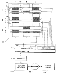
Figure 7 is a partial schematic diagram of an exemplary interferometric
modulator
display, similar to that shown in Figure 2. In the embodiment of Figure 7,
each of the rows of the
pixel array 30 is subdivided into three subrows, A, B, and C. Each of the
subrows defines one
interferometric modulator display element 100 at each column. The subrows are
each connected
to the row driver 24. As compared to Figure 2, the row driver 24 thus includes
additional
connections to the subrows to drive the color or greyscale pixel array 30. In
Figure 7, the display
elements 100 are each illustrated in exemplary reflecting (white) or absorbing
(hashed) states.
In the embodiment of Figure 7, the processor 21 is in communication with a
network
interface 102 that communicates over a network 104 with a content server 106.
The network
interface 102 may support communication over any suitable data communications
network. In
one embodiment, the network interface 102 is a cellular radio transceiver that
supports a code
division multiple access (CDMA), or other wireless voice and/or data
communications protocol
such as time division multiple access (TDMA), frequency division multiple
access (FDMA), or
Global System for Mobile Communications (GSM). In other embodiments, the
network interface
102 may support one or more additional, or alternative, radio interface
protocols such as
Bluetooth, IEEE 802.11, or other wireless protocols. In one embodiment, the
network interface
102 supports a wired data interface, such as Ethernet, a serial port, a
universal serial bus (USB)
-9-
CA 02520352 2005-09-21
port, Firewire, IEEE 1394, a synchronization cradle coupled to a network or
other computing
device, or an interface to a GPS receiver.
The network 104 may include an Internet Protocol (IP) network, wireless
networks, or
any other suitable data communications network. The content server 106 may
include any
suitable computer system configured to transmit image data, including motion
picture data in any
format suitable for transmission over the network 106.
In one embodiment, the array controller 22 controls the rate of update of the
display
elements 100. The processor 21 may configure the refresh rate of the array
controller 22. In one
embodiment, the array controller is configured to operate in two or more modes
of update. In one
mode, each of the rows of the pixel array 30 is updated using a method such as
described above
with reference to Figure SB. In a second mode, at least one of the subrows is
updated at a lower
frequency. For example, in one embodiment, in the second mode, subrows A and B
are updated
30 times a second and the remaining rows, e.g., subrow C is updated only once
a second. Thus,
power consumption is reduced with the tradeoff of lower color resolution and,
thus, color gamut
in the second mode. In another embodiment, the lower frequency of updating the
remaining
rows, e.g., row C, is very low, e.g., only when the display is initialized, or
when the mode
changes.
In one embodiment, the array controller 22 is configured to update the rows
and subrows
of display elements 100 by applying a series of row voltage strobes to each
subrow to configure
the state of the subrow. In one embodiment, in the second mode, the array
controller 22 is
configured to skip row voltage strobes for some of the subrows. For example,
in one
embodiment, in the first mode, the array controller 22 applies a series of row
voltage strobes to
each of the subrows A, B, and C of each row. When switched to the second mode,
the array
control 22 applies the row voltage strobes to subrows A and B of each row but
skips subrow C.
In one embodiment, as available battery power becomes lower, the array
controller 22 skips more
subrows, for example, by applying row voltage strobes to subrows A but
skipping subrows B and
C of each of the rows. In one embodiment, the array controller 22 applies a
series of row voltage
strobes to configure the states the non-updated subrows to a selected state,
e.g., non-reflecting,
upon entering the second mode. In one embodiment, the array controller 22
maintains the non-
updated subrows in the selected state by applying a bias voltage across the
display elements 100
of such subrows. In another embodiment, the array controller 22 periodically
applies row voltage
strobes to the otherwise non-updated subrows in the second mode to configure
the state of the
display elements 100 in such subrows to a new selected state. For example, the
array controller
22 periodically fails to skip the subrows C and updates the display elements
100 in the subrows C
to a new selected state. This periodic application of row voltage strobes to
the otherwise non-
updated subrows may be at a frequency much lower than the frequency of
application of row
-10-
CA 02520352 2005-09-21
voltage strobes to the other subrows. In one embodiment, the lower frequency
period is non-
constant. In one embodiment, the lower frequency period is based on image data
and varies
based on the image data.
In one embodiment, the display elements 100 of the subrows that are updated at
the lower
frequency, e.g., row C in the exemplary embodiment, are all set to the same
state. In one such
embodiment, the display elements of the less frequently updated subrows are
set to a non-
reflecting state. In another embodiment, the less frequently updated subrows
are set to display an
overall average visual shade of grey or color that may, for example, be based
on an average
brightness or color for some or all display elements 100 calculated over one
or more image frame
or frame portions.
In another embodiment, the display state of the less frequently updated
subrows of
display elements is based on particular portions of the image data stream. For
example, motion
video data, e.g., MPEG data, comprises reference frames describing all pixels
that are sent
relatively infrequently and intervening data frames that update only a portion
of the pixels in the
video image. In one embodiment, the less frequently updated subrows may be
updated only when
reference frames are displayed, and may be held at a particular state until
the next reference
frame is received. The particular state may be a calculated state, as
described above, or the actual
state for the less frequently updated display elements 100 in the reference
state.
In one embodiment, additional modes may include updating a different number of
subrows at different frequencies. For example, in one embodiment, in a first
mode each of
subrows A, B, and C is updated at a first rate; in a second mode, subrow A and
B are updated at a
first rate and subrow C at a lower rate, or at varying rate, such as described
above based on
receiving video reference data frames; and in a third mode, subrow A is
updated at a first rate,
subrow B at a second rate, and subrow C at a third rate. It is to be
recognized that in
embodiments with more subrows, additional modes of operation may be defined to
have varying
power consumption properties.
In one embodiment, the array controller 22 changes the display mode when
available
power level conditions, such as from a battery (not shown) providing power to
the array 30, fall
below a threshold level, or satisfy other predetermined conditions. In one
embodiment, the
processor 21 determines when to change display mode and signals the array
controller 22 to
change operational mode. In another embodiment, a user of an electronic device
that contains the
pixel array 30 may trigger the change to a different mode manually, or may
configure the device
to switch between modes under predetermined conditions.
In is to be recognized that while certain embodiments are discussed herein
with respect to
reducing display resolution by skipping row strobes, in other embodiments,
updates of particular
columns may be skipped to reduce power consumption. For example, in one such
embodiment,
CA 02520352 2005-09-21
rather than transitioning column voltages as image data for a given column
changes from row to
row, the voltage applied to some columns may be held at a potential that
maintains the display
elements of the skipped columns in an actuated or released state. In the
embodiment of Figure 5,
for example, the columns in which column transitions are skipped can be held
at a constant 0 V -
5 V to remain released during frame updates, or at a constant 10 V - 15 V to
remain activated
during frame updates.
In one embodiment, the image data being displayed by the display array 30
includes data
being received over the network 104 from the content server 106. In one
embodiment, the
processor 21 communicates data describing the current display mode being used
by the array
controller to the content server 106. The content server 106 may thus filter
the image data so that
the image data for non-updated display elements is not sent. Thus, the total
bandwidth consumed
by the communicated data signal is reduced in proportion to the number of
display elements that
are not being updated at the fastest display rate. This reduction in data rate
may further reduce
power consumption associated with the display as the network interface 102 and
the processor 21
have less data to process. In one embodiment, the content server 106 may
determine the state,
shade, or color for the less frequently updated subrows to display between
updates and
communicate that state to the processor 21.
In addition to varying the data rate based on the operational mode of the
display, the
content server 106 may also control or select the operational mode of the
array 30. For example,
based on information available to the content server 106 such as operational
or power data
associated with the display array 30 or controller 22, the content server 106
may send control
data to the processor 21 for selecting the operational mode of the array 30.
The content server
106 may also select the operational mode based on other data such as stored
user preferences,
rules associated with the content, or the desired rate of transfer of data on
the network 104.
Figures 8A and 8B are system block diagrams illustrating an embodiment of a
display
device 2040. The display device 2040 can be, for example, a cellular or mobile
telephone.
However, the same components of display device 2040 or slight variations
thereof are also
illustrative of various types of display devices such as televisions and
portable media players.
The display device 2040 includes a housing 2041, a display 2030, an antenna
2043, a
speaker 2045, an input device 2048, and a microphone 2046. The housing 2041 is
generally
formed from any of a variety of manufacturing processes as are well known to
those of skill in
the art, including injection molding, and vacuum forming. In addition, the
housing 2041 may be
made from any of a variety of materials, including but not limited to plastic,
metal, glass, rubber,
and ceramic, or a combination thereof. In one embodiment the housing 2041
includes removable
portions (not shown) that may be interchanged with other removable portions of
different color,
or containing different logos, pictures, or symbols.
-12-
CA 02520352 2005-09-21
The display 2030 of exemplary display device 2040 may be any of a variety of
displays,
including a bi-stable display, as described herein. In other embodiments, the
display 2030
includes a flat-panel display, such as plasma, EL, OLED, STN LCD, or TFT LCD
as described
above, or a non-flat-panel display, such as a CRT or other tube device, as is
well known to those
of skill in the art. However, for purposes of describing the present
embodiment, the display 2030
includes an interferometric modulator display, as described herein.
The components of one embodiment of exemplary display device 2040 are
schematically
illustrated in Figure 8B. The illustrated exemplary display device 2040
includes a housing 2041
and can include additional components at least partially enclosed therein. For
example, in one
embodiment, the exemplary display device 2040 includes a network interface
2027 that includes
an antenna 2043 which is coupled to a transceiver 2047. The transceiver 2047
is connected to the
processor 2021, which is connected to conditioning hardware 2052. The
conditioning hardware
2052 may be configured to condition a signal (e.g. filter a signal). The
conditioning hardware
2052 is connected to a speaker 2045 and a microphone 2046. The processor 2021
is also
connected to an input device 2048 and a driver controller 2029. The driver
controller 2029 is
coupled to a frame buffer 2028 and to the array driver 2022, which in turn is
coupled to a display
array 2030. A power supply 2050 provides power to all components as required
by the particular
exemplary display device 2040 design.
The network interface 2027 includes the antenna 2043 and the transceiver 2047
so that
the exemplary display device 2040 can communicate with one or more devices
over a network.
In one embodiment the network interface 2027 may also have some processing
capabilities to
relieve requirements of the processor 2021. The antenna 2043 is any antenna
known to those of
skill in the art for transmitting and receiving signals. In one embodiment,
the antenna transmits
and receives RF signals according to the IEEE 802.11 standard, including IEEE
802.11 (a), (b), or
(g). In another embodiment, the antenna transmits and receives RF signals
according to the
BLUETOOTH standard. In the case of a cellular telephone, the antenna is
designed to receive
CDMA, GSM, AMPS or other known signals that are used to communicate within a
wireless cell
phone network. The transceiver 2047 pre-processes the signals received from
the antenna 2043
so that they may be received by and further manipulated by the processor 2021.
The transceiver
2047 also processes signals received from the processor 2021 so that they may
be transmitted
from the exemplary display device 2040 via the antenna 2043.
In an alternative embodiment, the transceiver 2047 can be replaced by a
receiver. In yet
another alternative embodiment, network interface 2027 can be replaced by an
image source,
which can store or generate image data to be sent to the processor 2021. For
example, the image
source can be a digital video disc (DVD) or a hard-disc drive that contains
image data, or a
software module that generates image data.
-13-
CA 02520352 2005-09-21
Processor 2021 generally controls the overall operation of the exemplary
display device
2040. The processor 2021 receives data, such as compressed image data from the
network
interface 2027 or an image source, and processes the data into raw image data
or into a format
that is readily processed into raw image data. The processor 2021 then sends
the processed data
to the driver controller 2029 or to frame buffer 2028 for storage. Raw data
typically refers to the
information that identifies the image characteristics at each location within
an image. For
example, such image characteristics can include color, saturation, and gray-
scale level.
In one embodiment, the processor 2021 includes a microcontroller, CPU, or
logic unit to
control operation of the exemplary display device 2040. Conditioning hardware
2052 generally
includes amplifiers and filters for transmitting signals to the speaker 2045,
and for receiving
signals from the microphone 2046. Conditioning hardware 2052 may be discrete
components
within the exemplary display device 2040, or may be incorporated within the
processor 2021 or
other components.
The driver controller 2029 takes the raw image data generated by the processor
2021
either directly from the processor 2021 or from the frame buffer 2028 and
reformats the raw
image data appropriately for high speed transmission to the array driver 2022.
Specifically, the
driver controller 2029 reformats the raw image data into a data flow having a
raster-like format,
such that it has a time order suitable for scanning across the display array
2030. Then the driver
controller 2029 sends the formatted information to the array driver 2022.
Although a driver
controller 2029, such as a LCD controller, is often associated with the system
processor 2021 as a
stand-alone Integrated Circuit (IC), such controllers may be implemented in
many ways. They
may be embedded in the processor 2021 as hardware, embedded in the processor
2021 as
software, or fully integrated in hardware with the array driver 2022.
Typically, the array driver 2022 receives the formatted information from the
driver
controller 2029 and reformats the video data into a parallel set of waveforms
that are applied
many times per second to the hundreds and sometimes thousands of leads coming
from the
display's x-y matrix of pixels.
In one embodiment, the driver controller 2029, array driver 2022, and display
array 2030
are appropriate for any of the types of displays described herein. For
example, in one
embodiment, driver controller 2029 is a conventional display controller or a
bi-stable display
controller (e.g., an interferometric modulator controller). In another
embodiment, array driver
2022 is a conventional driver or a bi-stable display driver (e.g., an
interferometric modulator
display). In one embodiment, a driver controller 2029 is integrated with the
array driver 2022.
Such an embodiment is common in highly integrated systems such as cellular
phones, watches,
and other small area displays. In yet another embodiment, display array 2030
is a typical display
-14-
CA 02520352 2005-09-21
array or a bi-stable display array (e. g., a display including an array of
interferometric
modulators).
The input device 2048 allows a user to control the operation of the exemplary
display
device 2040. In one embodiment, input device 2048 includes a keypad, such as a
QWERTY
keyboard or a telephone keypad, a button, a switch, a touch-sensitive screen,
a pressure- or heat-
sensitive membrane. In one embodiment, the microphone 2046 is an input device
for the
exemplary display device 2040. When the microphone 2046 is used to input data
to the device,
voice commands may be provided by a user for controlling operations of the
exemplary display
device 2040.
Power supply 2050 can include a variety of energy storage devices as are well
known in
the art. For example, in one embodiment, power supply 2050 is a rechargeable
battery, such as a
nickel-cadmium battery or a lithium ion battery. In another embodiment, power
supply 2050 is a
renewable energy source, a capacitor, or a solar cell, including a plastic
solar cell, and solar-cell
paint. In another embodiment, power supply 2050 is configured to receive power
from a wall
outlet.
In some implementations control programmability resides, as described above,
in a driver
controller which can be located in several places in the electronic display
system. In some cases
control programmability resides in the array driver 2022. Those of skill in
the art will recognize
that the above-described optimization may be implemented in any number of
hardware and/or
software components and in various configurations.
While the above detailed description has shown, described, and pointed out
novel
features of the invention as applied to various embodiments, it will be
understood that various
omissions, substitutions, and changes in the form and details of the device or
process illustrated
may be made by those skilled in the art without departing from the spirit of
the invention. As will
be recognized, the present invention may be embodied within a form that does
not provide all of
the features and benefits set forth herein, as some features may be used or
practiced separately
from others. The scope of the invention is indicated by the appended claims
rather than by the
foregoing description. All changes which come within the meaning and range of
equivalency of
the claims are to be embraced within their scope.
-15-