Note: Descriptions are shown in the official language in which they were submitted.
CA 02520358 2005-09-21
Internal Reference: IRDM.055 NON-EP / IDC-040018
SYSTEM AND METHOD FOR PROTECTING MICRO-STRUCTURE OF DISPLAY
ARRAY USING SPACERS IN GAP WITHIN DISPLAY DEVICE
Background
Field of the Invention
The invention relates to electronic devices. More particularly, the invention
relates to a
packaging system and a method for protecting a microelectromechanical device
from physical
damage.
Description of the Related Technology
Microelectromechanical systems (MEMS) include micromechanical elements,
actuators,
and electronics. Micromechanical elements may be created using deposition,
etching, and or
other micromachining processes that etch away parts of substrates and/or
deposited material
layers or that add layers to form electrical and electromechanical devices.
One type of MEMS
device is called an interferometric modulator. An interferometric modulator
may comprise a pair
of conductive plates, one or both of which may be transparent and/or
reflective in whole or part
and capable of relative motion upon application of an appropriate electrical
signal. One plate
may comprise a stationary layer deposited on a substrate, the other plate may
comprise a metallic
membrane separated from the stationary layer by an air gap. Such devices have
a wide range of
applications, and it would be beneficial in the art to utilize and/or modify
the characteristics of
these types of devices so that their features can be exploited in improving
existing products and
creating new products that have not yet been developed.
Summary
One embodiment of the invention is a display device comprising an array of
interferometric modulators formed on a substrate. This embodiment includes a
backplate and a
seal disposed between the substrate and the backplate, wherein the substrate
and backplate seal
together to package the array of interferometric modulators. One or more
spacers are disposed
between the array and the backplate, wherein the one or more spacers prevent
the backplate from
contacting the array.
Another embodiment of the invention is a method for making a display device.
This
embodiment includes providing an interferometric modulator array on a
substrate and disposing
one or more spacers on the substrate. The method also provides sealing a
backplate onto the
substrate to form a display device, wherein the one or more spacers prevent
the backplate from
contacting the array.
-1-
CA 02520358 2005-09-21
Still another embodiment of the invention is a display device made by the
method of
providing an interferometric modulator array on a substrate and disposing one
or more spacers on
the substrate. The method of making the display device also includes sealing a
backplate onto the
substrate to form a display device, wherein the one or more spacers prevent
the backplate from
contacting the array.
One other embodiment of the invention is a display device. In this embodiment,
the
display device includes transmissive means for transmitting light therethrough
and modulating
means for modulating light transmitter through the transmissive means. The
display device also
comprises covering means for covering the modulating means and sealing means
disposed
between the transmissive means and the covering means to form a package. Also,
the display
device includes spacing means for preventing the modulating means and the
covering means from
contacting each other within the display device.
Brief Description of the Drawings
These and other aspects of the invention will be readily apparent from the
following
description and from the appended drawings (not to scale), which are meant to
illustrate and not
to limit the invention.
FIG. 1 is an isometric view depicting a portion of one embodiment of an
interferometric
modulator display in which a movable reflective layer of a first
interferometric modulator is in a
released position and a movable reflective layer of a second interferometric
modulator is in an
actuated position.
FIG. 2 is a system block diagram illustrating one embodiment of an electronic
device
incorporating a 3 x 3 interferometric modulator display.
FIG. 3 is a diagram of movable mirror position versus applied voltage for one
exemplary
embodiment of an interferometric modulator of FIG. 1.
FIG. 4 is an illustration of sets of row and column voltages that may be used
to drive an
interferometric modulator display.
FIG. SA il lustrates one exemplary frame of display data in the 3x3
interferometric
modulator display of FIG. 2.
FIG. 5B illustrates one exemplary timing diagram for row and column signals
that may
be used to write the frame of FIG. SA.
FIG. 6A is a cross section of the device of FIG. 1. FIG. 6B is a cross section
of an
alternative embodiment of an interferometric modulator. FIG. 6C is a cross
section of an
alternative embodiment of an interferometric modulator.
FIG. 7A and FIG. 7B illustrate an exploded view and a cross section of an
embodiment
of a display package comprising a spacer. FIG. 7C illustrates an embodiment of
a display
-2-
CA 02520358 2005-09-21
package comprising a recessed cap. FIG. 7D illustrates an embodiment of a
display package that
comprises a curved backplate.
FIG. 8A illustrates a cross section of an embodiment of a recessed cap. FIG.
8B
illustrates a cross section of an embodiment of a backplate comprising
reinforcing ribs. FIG. 8C
illustrates a cross section of an embodiment of a recessed cap comprising
reinforcing ribs.
FIG. 8D a nd FIG. 8E illustrate in cross section backplates comprising
cavities in which a
desiccant is disposed.
FIG. 9 illustrates a cross section of a double array device, which comprises
two
interferometric modulator arrays.
FIG. 10 illustrates a cross section of an embodiment of a display package
comprising a
desiccant.
FIG. 11A illustrates a top view of an embodiment of a device in which the
spacers are
arranged in a substantially regular pattern. FIG. 11B illustrates a top view
of an embodiment of
a device in which the spacers are arranged in a random pattern. FIG. 11C
illustrates a top view
IS of an embodiment of a device in which the spacers are arranged around the
center of the array.
FIG. 11D illustrates a top view of an embodiment of a device in which the
spacers are more
dense around the center of the array and less dense around the periphery. FIG.
11E illustrates a
top view of an embodiment of a device comprising three concentric zones of
spacers.
FIG. 12A - FIG. 12T illustrate embodiments of spacers.
FIG. 13A illustrates a top view of an embodiment of a device comprising
spacers that
span at least two posts in the array. FIG. 13B illustrates a top view of an
embodiment of a device
comprising disk-shaped spacers that span at least two posts in the array.
FIG. 14 illustrates a top view of an embodiment of a device comprising spacers
at least
as large as an interferometric modulator element in an array.
FIG. 15A il lustrates a top view of an embodiment of a device comprising
spacers
substantially centered over the posts. FIG. 15B illustrates a top view of an
embodiment of a
device wherein a portion of each spacer is positioned over a post. FIG. 15C
illustrates a top view
of an embodiment of a device wherein no portion of any spacer is positioned
over a post.
FIG. 16 illustrates a top view of an embodiment of a device comprising spacers
of
different sizes.
FIG. 17A illustrates a top view of an embodiment of a device comprising a mesh
spacer.
FIG. 17B illustrates a top view of an embodiment of a device comprising a mesh
spacer that is
denser at the center than at the periphery. FIG. 17C illustrates a top view of
an integrated
rectangular spacer. FIG. 17D illustrates a top view of an integrated diagonal
spacer.
-3-
CA 02520358 2005-09-21
FIG. 18A illustrates a cross section of an embodiment of a device comprising a
film
spacer. FIG. 18B illustrates a cross section of an embodiment of a device
comprising a film
spacer with a non-planar cross section. FIG. 18C illustrates a cross section
of an embodiment of
a device comprising a film spacer in the form of a bag.
FIG. 19 illustrates a cross section of an embodiment of a device comprising a
plurality of
film spacers.
FIG. 20A - FIG. 20D illustrate in cross section the response of an embodiment
of a
spacer with a triangular cross section to an applied force. FIG. 20E
illustrates an embodiment of
a spacer with a thinner upper portion and a thicker lower portion. FIG. 20F
illustrates a cross
section of an embodiment of a spacer with two regions that respond differently
to an applied
force.
FIG. 21A illustrates a cross section of an embodiment of a device in which the
spacer
extends between the array and backplate. FIG. 21B illustrates a cross section
of an embodiment
of a device in which the spacer contacts the array but not the backplate. FIG.
21C illustrates a
cross section of an embodiment of a device in which the spacer contacts the
backplate but not the
array.
FIG. 22A illustrates a cross section of an embodiment of a device comprising
integrated
spacers formed over the posts of the interferometric modulators. FIG. 22B
illustrates a cross
section of an embodiment of a device comprising integrated spacers formed over
the posts of
interferometric modulators of different heights and a second spacer disposed
on the integrated
spacers. FIG. 22C illustrates a cross section of an embodiment of a device
comprising integrated
spacers formed over the posts of interferometric modulators and a second
spacer that engages the
integrated spacers.
FIG. 23 is a flowchart illustrating an embodiment of a method for
manufacturing an
packaged electronic device that resists physical damage.
FIG. 24 is a flowchart illustrating an embodiment of a method for protecting
an
electronic device from physical damage.
FIGS. 25A and 25B are system block diagrams illustrating an embodiment of a
visual
display device comprising a plurality of interferometric modulators.
Detailed Description of Certain Embodiments
Electronic devices are susceptible to damage from physical assaults, for
example, drops,
twisting, impacts, pressure, and the like. Some devices are more sensitive to
damage than others.
For example, devices with moving parts are susceptible to displacement or
breakage of one or
more of the moving parts. Some microelectromechanical system (MEMS) devices
are
-4-
CA 02520358 2005-09-21
particularly sensitive to physical assaults because of the fine dimensions of
their components.
Consequently, such devices are typically packaged to reduce or prevent
undesired contacts, which
can damage to the device.
In some cases, the packaging itself is distorted or deformed by external
forces, which
cause components of the packaging to contact, and in some cases, damage or
impair the operation
of the device packaged therein. Accordingly, disclosed herein is a packing
system for electronic
devices, including MEMS devices, that includes spacers configured to prevent
or reduce contacts
of components in the packaged device likely to damage the electronic device.
In some
embodiments, the spacers are configured to prevent or reduce damage arising
from contacts
between the array of interferometric modulators and the backplate of a
packaging system for the
same. Consequently, in some embodiments, a package display comprising one or
more spacers is
thinner than an equivalent package display fabricated without spacers because
the spacers permit
disposing the backplate closer to the interferometric modulator array, as
discussed below.
The interferometric modulator MEMS devices disclosed herein are useful in the
fabrication of display devices. In some embodiments, the display comprises an
array of
interferometric modulators formed on a substrate, thereby producing a device
that is relatively
thin compared to its length and/or width. Some embodiments of such structures
are susceptible
to deflection or deformation by a force with a component that is normal to the
surface of the
device. Some embodiments of such structures are susceptible to deformation on
torsion. Those
skilled in the art will understand that, all other things being equal, the
deflection or deformation
will increase with increasing length and/or width of the device.
Forces likely to induce such deflections and/or deformations are not unusual
in portable
electronic devices. Such forces arise in touch screen applications, for
example, or in stylus-based
interfaces. Furthermore, it is common for users to touch or press on the
surface of a display, for
example, when pointing out an image on a computer display. Inadvertent contact
of the display
also occurs, for example, on a mobile telephone display in a user's pocket or
purse.
The following detailed description is directed to certain specific embodiments
of the
invention. However, the invention can be embodied in a multitude of different
ways. In this
description, reference is made to the drawings wherein like parts are
designated with like
numerals throughout. As will be apparent from the following description, the
invention may be
implemented in any device that is configured to display an image, whether in
motion (e.g., video)
or stationary (e.g., still image), and whether textual or pictorial. More
particularly, it is
contemplated that the invention may be implemented in or associated with a
variety of electronic
devices such as, but not limited to, mobile telephones, wireless devices,
personal data assistants
(PDAs), hand-held or portable computers, GPS receivers/navigators, cameras,
MP3 players,
camcorders, game consoles, wrist watches, clocks, calculators, television
monitors, flat panel
-5-
CA 02520358 2005-09-21
displays, computer monitors, auto displays (e.g., odometer display, etc.),
cockpit controls and/or
displays, display of camera views (e.g., display of a rear view camera in a
vehicle), electronic
photographs, electronic billboards or signs, projectors, architectural
structures, packaging, and
aesthetic structures (e.g., display of images on a piece of jewelry). MEMS
devices of similar
structure to those described herein can also be used in non-display
applications such as in
electronic switching devices.
One interferometric modulator display embodiment comprising an interferometric
MEMS display element is illustrated in FIG. 1. In these devices, the pixels
are in either a bright
or dark state. In the bright ("on" or "open") state, the display element
reflects a large portion of
incident visible light to a user. When in the dark ("off' or "closed") state,
the display element
reflects little incident visible light to the user. Depending on the
embodiment, the light
reflectance properties of the "on" and "off ' states may be reversed. MEMS
pixels can be
configured to reflect predominantly at selected colors, allowing for a color
display in addition to
black and white.
FIG. 1 is an isometric view depicting two adjacent pixels in a series of
pixels of a visual
display, wherein each pixel comprises a MEMS interferometric modulator. In
some
embodiments, an interferometric modulator display comprises a row/column array
of these
interferometric modulators. Each interferometric modulator includes a pair of
reflective layers
positioned at a variable and controllable distance from each other to form a
resonant optical
cavity with at least one variable dimension. In one embodiment, one of the
reflective layers may
be moved between two positions. In the first position, referred to herein as
the released state, the
movable layer is positioned at a relatively large distance from a fixed
partially reflective layer. In
the second position, the movable layer is positioned more closely adjacent to
the partially
reflective layer. Incident light that reflects from the two layers interferes
constructively or
destructively depending on the position of the movable reflective layer,
producing either an
overall reflective or non-reflective state for each pixel.
The depicted portion of the pixel array in FIG. 1 includes two adjacent
interferometric
modulators 12a and 12b. In the interferometric modulator 12a on the left, a
movable and highly
reflective layer 14a is illustrated in a released position at a predetermined
distance from a fixed
partially reflective layer 16a. In the interferometric modulator 12b on the
right, the movable
highly reflective layer 14b is illustrated in an actuated position adjacent to
the fixed partially
reflective layer 16b.
The fixed layers 16a, 16b are electrically conductive, partially transparent
and partially
reflective, and may be fabricated, for example, by depositing one or more
layers each of
chromium and indium-tin-oxide onto a transparent substrate 20. The layers are
patterned into
parallel strips, and may form row electrodes in a display device as described
further below. The
-6-
CA 02520358 2005-09-21
movable layers 14a, 14b may be formed as a series of parallel strips of a
deposited metal layer or
layers (orthogonal to the row electrodes 16a, 16b) deposited on top of posts
18 and an
intervening sacrificial material deposited between the posts 18. When the
sacrificial material is
etched away, the deformable metal layers are separated from the fixed metal
layers by a defined
air gap 19. A highly conductive and reflective material such as aluminum may
be used for the
deformable layers, and these strips may form column electrodes in a display
device.
With no applied voltage, the cavity 19 remains between the layers 14a, 16a and
the
deformable layer is in a mechanically relaxed state as illustrated by the
pixel 12a in FIG. 1.
However, when a potential difference is applied to a selected row and column,
the capacitor
formed at the intersection of the row and column electrodes at the
corresponding pixel becomes
charged, and electrostatic forces pull the electrodes together. If the voltage
is high enough, the
movable layer is deformed and is forced against the fixed layer (a dielectric
material which is not
illustrated in this Figure may be deposited on the fixed layer to prevent
shorting and control the
separation distance) as illustrated by the pixel 12b on the right in FIG. 1.
The behavior is the
same regardless of the polarity of the applied potential difference. In this
way, row/column
actuation that can control the reflective vs. non-reflective pixel states is
analogous in many ways
to that used in conventional LCD and other display technologies.
FIG. 2 through FIG. SB illustrate one exemplary process and system for using
an array
of interferometric modulators in a display application. FIG. 2 is a system
block diagram
illustrating one embodiment of an electronic device that may incorporate
aspects of the invention.
In the exemplary embodiment, the electronic device includes a processor 21
which may be any
general purpose single- or mufti-chip microprocessor such as an ARM, Pentium~,
Pentium II~,
Pentium III~, Pentium IV~, Pentium~ Pro, an 8051, a MIPS~, a Power PC~, an
ALPHA~, or any
special purpose microprocessor such as a digital signal processor,
microcontroller, or a
programmable gate array. As is conventional in the art, the processor 21 may
be configured to
execute one or more software modules. In addition to executing an operating
system, the
processor may be configured to execute one or more software applications,
including a web
browser, a telephone application, an email program, or any other software
application.
In one embodiment, the processor 21 is also configured to communicate with an
array
controller 22. In one embodiment, the array controller 22 includes a row
driver circuit 24 and a
column driver circuit 26 that provide signals to a pixel array 30. The cross
section of the array
illustrated in FIG. 1 is shown by the lines 1-1 in FIG. 2. For MEMS
interferometric modulators,
the row/column actuation protocol may take advantage of a hysteresis property
of these devices
illustrated in FIG. 3. It may require, for example, a 10 volt potential
difference to cause a
movable layer to deform from the released state to the actuated state.
However, when the voltage
is reduced from that value, the movable layer maintains its state as the
voltage drops back below
CA 02520358 2005-09-21
volts. In the exemplary embodiment of FIG. 3, the movable layer does not
release completely
until the voltage drops below 2 volts. There is thus a range of voltage, about
3 to 7 V in the
example illustrated in FIG. 3, where there exists a window of applied voltage
within which the
device is stable in either the released or actuated state. This is referred to
herein as the
5 "hysteresis window" or "stability window." For a display array having the
hysteresis
characteristics of FIG. 3, the row/column actuation protocol can be designed
such that during
row strobing, pixels in the strobed row that are to be actuated are exposed to
a voltage difference
of about 10 volts, and pixels that are to be released are exposed to a voltage
difference of close to
zero volts. After the strobe, the pixels are exposed to a steady state voltage
difference of about 5
10 volts such that they remain in whatever state the row strobe put them in.
After being written,
each,pixel sees a potential difference within the "stability window" of 3-7
volts in this example.
This feature makes the pixel design illustrated in FIG. 1 stable under the
same applied voltage
conditions in either an actuated or released pre-existing state. Since each
pixel of the
interferometric modulator, whether in the actuated or released state, is
essentially a capacitor
formed by the fixed and moving reflective layers, this stable state can be
held at a voltage within
the hysteresis window with almost no power dissipation. Essentially no current
flows into the
pixel if the applied potential is fixed.
In typical applications, a display frame may be created by asserting the set
of column
electrodes in accordance with the desired set of actuated pixels in the first
row. A row pulse is
then applied to the row 1 electrode, actuating the pixels corresponding to the
asserted column
lines. The asserted set of column electrodes is then changed to correspond to
the desired set of
actuated pixels in the second row. A pulse is then applied to the row 2
electrode, actuating the
appropriate pixels in row 2 in accordance with the asserted column electrodes.
The row 1 pixels
are unaffected by the row 2 pulse, and remain in the state they were set to
during the row 1 pulse.
This may be repeated for the entire series of rows in a sequential fashion to
produce the frame.
Generally, the frames are refreshed and/or updated with new display data by
continually
repeating this process at some desired number of frames per second. A wide
variety of protocols
for driving row and column electrodes of pixel arrays to produce display
frames are also well
known and may be used in conjunction with the present invention.
FIG. 4, FIG. SA and FIG. 5B illustrate one possible actuation protocol for
creating a
display frame on the 3 X 3 array of FIG. 2. FIG. 4 illustrates a possible set
of column and row
voltage levels that may be used for pixels exhibiting the hysteresis curves of
FIG. 3. In the
FIG. 4 embodiment, actuating a pixel involves setting the appropriate column
to -Vb;$S, and the
appropriate row to +~V, which may correspond to -5 volts and +5 volts
respectively Releasing
the pixel is accomplished by setting the appropriate column t0 +Vb;as, and the
appropriate row to
the same +OV, producing a zero volt potential difference across the pixel. In
those rows where
_g_
CA 02520358 2005-09-21
the row voltage is held at zero volts, the pixels are stable in whatever state
they were originally
in, regardless of whether the column is at +Vb;as, or -Vb;as~
FIG. SB is a timing diagram showing a series of row and column signals applied
to the 3
X 3 array of FIG. 2 which will result in the display arrangement illustrated
in FIG. SA, where
actuated pixels are non-reflective. Prior to writing the frame illustrated in
FIG. SA, the pixels
can be in any state, and in this example, all the rows are at 0 volts, and all
the columns are at +5
volts. With these applied voltages, all pixels are stable in their existing
actuated or released
states.
In the FIG. SA frame, pixels (1,1), (1,2), (2,2), (3,2) and (3,3) are
actuated. To
accomplish this, during a "line time" for row 1, columns 1 and 2 are set to -5
volts, and column 3
is set to +5 volts. This does not change the state of any pixels, because all
the pixels remain in
the 3; 7 volt stability window. Row 1 is then strobed with a pulse that goes
from 0, up to 5 volts,
and back to zero. This actuates the (1,1) and (1,2) pixels and releases the
(1,3) pixel. No other
pixels in the array are affected. To set row 2 as desired, column 2 is set to -
5 volts, and columns
1 and 3 are set to +5 volts. The same strobe applied to row 2 will then
actuate pixel (2,2) and
release pixels (2,1) and (2,3). Again, no other pixels of the array are
affected. Row 3 is similarly
set by setting columns 2 and 3 to -5 volts, and column 1 to +S volts. The row
3 strobe sets the
row 3 pixels as shown in FIG. SA. After writing the frame, the row potentials
are zero, and the
column potentials can remain at either +5 or -5 volts, and the display is then
stable in the
arrangement of FIG. SA. It will be appreciated that the same procedure can be
employed for
arrays of dozens or hundreds of rows and columns. It will also be appreciated
that the timing,
sequence, and levels of voltages used to perform row and column actuation can
be varied widely
within the general principles outlined above, and the above example is
exemplary only, and any
actuation voltage method can be used with the present invention.
The details of the structure of interferometric modulators that operate in
accordance with
the principles set forth above may vary widely. For example, FIG. 6A - FIG. 6C
illustrate three
different embodiments of the moving mirror structure. FIG. 6A i s a cross
section of the
embodiment of FIG. 1, Error! Reference source not found.where a strip of metal
material 14 is
deposited on orthogonally extending supports 18. In FIG. 6B, the moveable
reflective material
14 is. attached to supports at the corners only, on tethers 32. In FIG. 6C,
the moveable reflective
material 14 is suspended from a deformable layer 34. This embodiment has
benefits because the
structural design and materials used for the reflective material 14 can be
optimized with respect
to the optical properties, and the structural design and materials used for
the deformable layer 34
can be optimized with respect to desired mechanical properties. The production
of various types
of interferometric devices is described in a variety of published documents,
including, for
example, U.S. Published Application 2004/0051929. A wide variety of well known
techniques
-9-
CA 02520358 2005-09-21
may be used to produce the above described structures involving a series of
material deposition,
patterning, and etching steps.
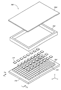
FIG. 7A and FIG. 7B illustrate an exploded view and cross-section of an
embodiment of
a packaged electronic device 700 comprising a substrate 710, an array 720 of
interferometric
modulators 722, one or more spacers 730, a seal 740, and a backplate 750. As
best seen in
FIG. 7B, the device 700 comprises a first side 702 and a second side 704. The
substrate 710
comprises a first surface 712 and a second surface 714. On the second surface
714 of the
substrate is formed the interferometric modulator array 720. In the
illustrated embodiment, the
backplate 750 is secured to the substrate 710 by the seal 740. Disposed
between the array 720
and the backplate 750 is one or more spacers 730. Also illustrated in FIG. 7A
are x, y, and z
axes, and in FIG. 7B, y and z axes referred to in the description herein.
The substrate 710 and interferometric modulators 722 are described in greater
detail
above. Briefly, the substrate 710 is any substrate on which an interferometric
modulator 722 is
formable. In some embodiments, the device 700 displays an image viewable from
the first side
702, and accordingly, the substrate 710 is substantially transparent and/or
translucent. For
example, in some embodiments, the substrate is glass, silica, and/or alumina.
In other
embodiments, the substrate 710 is not substantially transparent and/or
translucent, for example, in
a device 700 that displays an image viewable from the second side 704, or in a
device 700 that
does not display a viewable image. In some embodiments, the first surface 712
of the substrate
further comprises one or more additional structures, for example, one or more
structural,
protective, and/or optical films.
The interferometric modulators 722 are of any type. In some embodiments, the
interferometric modulator 722 comprises a mechanical layer 724 distal from the
substrate 710
and proximal to the backplate 750. As discussed in greater detail below, in
some embodiments,
the mechanical layer 724 is susceptible to physical damage.
In the illustrated embodiments, the seal 740 secures the backplate 750 to the
substrate
710. The term "perimeter support" is also used herein to refer to the seal
740. In the
embodiment illustrated in FIG. 7B, the seal 740 also acts to maintain a
predetermined spacing
between the backplate 750 and substrate 710. In the embodiment illustrated in
FIG. 7C, the seal
740' does not have a spacing function. In some embodiments, the seal does not
produce or outgas
a volatile compound, for example, hydrocarbons, acids, amines, and the like.
In some
embodiments, the seal is partially or substantially impermeable to liquid
water and/or water
vapor. In some embodiments, the seal is partially or substantially impermeable
to air and/or other
gases. In some embodiments, the seal is rigid. In other embodiments, the seal
is elastic or
elastomeric. In other embodiments, the seal comprises both rigid, and elastic
or elastomeric
-10-
CA 02520358 2005-09-21
components. In some embodiments, the seal comprises one or more adhesives
compatible with
the substrate and/or backplate. The adhesive or adhesives are of suitable any
type known in the
art. In some embodiments, one or more of the adhesives is pressure sensitive.
In some
embodiments, one or more of the adhesives is thermally cured. In some
embodiments, one or
more of the adhesives is UV-cured. In some embodiments, the seal is thermally
bonded to the
substrate and/or backplate. In some embodiments, the seal is secured to the
substrate and/or
backplate mechanically. Some embodiments use a combination of methods for
securing the seal
to the substrate and/or backplate. Some embodiments do not comprise a seal,
for example, where
the substrate is secured directly to the backplate, for example, by thermal
welding.
The seal comprises any suitable material, for example, metals, steel,
stainless steel, brass,
titanium, magnesium, aluminum, copper, tin, lead, zinc, solder, polymer
resins, epoxies,
polyamides, polyalkenes, polyesters, polysulfones, polystyrene, polyurethanes,
polyacrylates,
cyanoacrylates, acrylic epoxies, silicones, rubbers, polyisobutylene,
neoprene, polyisoprene,
styrene-butadiene, parylene, U.V.-curable adhesives, ceramics, glass, silica,
alumina, and blends,
copolymers, alloys, and/or composites thereof. In some embodiments, the seal
further comprises
a reinforcement, for example, fibers, a mesh, and/or a fabric, for example,
glass, metal, carbon,
boron, carbon nanotubes, and the like. In some embodiments, the selected seal
material is
partially or substantially water impermeable. Accordingly, in some
embodiments, the seal is a
semi-hermetic or hermetic seal. In some embodiments, the seal is less than
about 50 pm thick,
for example, from about 10 pm to about 30 pm thick. In some embodiments, the
seal is from
about 0.5 mm to about S mm wide, for example, from about 1 mm to about 2 mm.
Returning to FIG. 7A and FIG. 7B, an embodiment of a method for fabricating
the
illustrated seal 740 using a UV-curable epoxy is described below. The epoxy is
applied to the
backplate 750 and/or substrate 710 using means known in the art, for example,
by printing. The
type and amount of epoxy is preselected to provide a seal 740 with the desired
width, thickness,
and moisture permeation properties. The backplate 750 and substrate 710 are
brought together,
and the epoxy cured by irradiation with a suitable source of UV radiation. A
typical epoxy is
cured using about 6000 mJ/cm2 of UV radiation. Some embodiments also include a
post-cure
bake at about 80 °C.
The backplate 750 is also referred to herein as a "cap" or "backplane." These
terms are
not intended to limit the position of the backplate 750 within the device 700,
or the orientation of
the device 700 itself. In some embodiments, the backplate 750 protects the
array 720 from
damage. As discussed above, some embodiments of an interferometric modulator
722 are
potentially damaged by physical assaults. Consequently, in some embodiments,
the backplate
750 protects the array 720 from contact with foreign objects and/or other
components in an
apparatus comprising the array 720, for example. Furthermore, in some
embodiments, the
-I1-
CA 02520358 2005-09-21
backplate 750 protects the array 720 from other environmental conditions, for
example, humidity,
moisture, dust, changes in ambient pressure, and the like.
In embodiments in which the device 700 displays an image viewable from the
second
side 704, the backplate 750 is substantially transparent and/or translucent.
In other embodiments,
the backplate 750 is not substantially transparent and/or translucent. In some
embodiments, the
backplate 750 is made from a material that does not produce or outgas a
volatile compound, for
example, hydrocarbons, acids, amines, and the like. In some embodiments, the
backplate 750 is
substantially impermeable to liquid water and/or water vapor. In some
embodiments, the
backplate 750 is substantially impermeable to air and/or other gases. Suitable
materials for the
backplate 750 include, for example, metals, steel, stainless steel, brass,
titanium, magnesium,
aluminum, polymer resins, epoxies, polyamides, polyalkenes, polyesters,
polysulfones,
polystyrene, polyurethanes, polyacrylates, parylene, ceramics, glass, silica,
alumina, and blends,
copolymers, alloys, composites, and/or combinations thereof. Examples of
suitable composite
materials include composite films available from Vitex Systems (San Jose, CA).
In some
embodiments, the backplate 750 further comprises a reinforcement, for example,
fibers and/or a
fabric, for example, glass, metal, carbon, boron, carbon nanotubes, and the
like.
In some embodiments, the backplate 750 is substantially rigid. In other
embodiments, the
backplate 750 is flexible, for example, foil or film. In some embodiments, the
backplate 750 is
deformed in a predetermined configuration before and/or during assembly of the
package
structure 700. As will be discussed in greater detail below, in some
embodiments, the backplate
750 is an element in a system for preventing damage to the array 710.
The backplate 750 comprises an inner surface 752 and an outer surface 753. In
some
embodiments, the inner surface and/or outer surface of the backplate further
comprise one or
more additional structures, for example, a structural, protective, mechanical,
and/or optical film
or films.
In the embodiment illustrated in FIG. 7B, the backplate 750 is substantially
planar.
FIG. 7C illustrates an embodiment of a device 700' in which the inner surface
752' of the
backplate is recessed, thereby forming a flange 754' at the perimeter of the
backplate 750'. A
backplate with this configuration is referred to as a "recessed cap" herein.
FIG. 7D illustrates in cross section an embodiment of a package device 700"
comprising
a curved or bowed backplate 750". In the illustrated embodiment, spacers 730"
are disposed
near the periphery of an array 720", which is relatively closer to the
backplate 750", and
consequently, more likely to contact the backplate 750" and sustain damage.
Other embodiments
comprise a different configuration of one or more spacers. Spacers are
discussed in greater detail
below. In some embodiments, the backplate 750" is preformed into the curved
configuration. In
-12-
CA 02520358 2005-09-21
other embodiments, the curved shape of the backplate 750" is formed by bending
or deforming a
substantially flat precursor during assembly of the package device 700". For
example, in some
embodiments, an array 720" of interferometric modulators is formed on a
substrate 710" as
described above. A seal material, for example, a UV curable epoxy, is applied
to the periphery of
a substantially planar backplate 750", which is wider and/or longer than the
substrate 710". The
backplate 750" is deformed, for example, by compression, to the desired size,
and positioned on
the substrate 710". The epoxy is cured, for example, using UV radiation to
form the seal 740".
Other embodiments for the backplate are illustrated FIG. 8A - FIG. 8C. FIG. 8A
illustrates a recessed cap 850 in which the inner surface 852 is concave. In
the illustrated
embodiment, the inner surface 852 and the outer surface 853 are not parallel.
Consequently, the
recessed cap 850 is thinner at the center 858 than at the edge 859. Those
skilled in the art will
understand that other arrangements are possible. The illustrated embodiment
comprises a
peripheral flange 854, which sets the minimum spacing between the substrate
and the inner
surface 852 of the recessed cap backplate. In some embodiments, the peripheral
flange 854 forms
a substantially continuous structure around the periphery of the recessed cap
850. In other
embodiments, the peripheral flange 854 is not continuous. Other embodiments do
not comprise a
peripheral flange. In FIG. 8B, the backplate 850 comprises reinforcing ribs
856 on the outer
surface 853. In other embodiments, the reinforcing ribs are on the inner
surface 852 or on both
surfaces of the backplate. In some embodiments, the reinforcing structure has
another shape, for
example, a grid, or honeycomb. Some embodiments comprise a combination of
these features.
For example, FIG. 8C illustrates an embodiment of a recessed cap 850 with a
concave inner
surface 852 and reinforcing ribs 856 on the outer surface 853. Some
embodiments of the
disclosed backplates exhibit improved properties, for example, strength,
weight, cost, rigidity,
transparency, ease of manufacturing, and the like.
FIG. 8D and FIG. 8E illustrate in cross section backplates comprising one or
more
cavities configured to contain a desiccant. FIG. 8D illustrates an embodiment
of a backplate 850
comprising a cavity 857 formed on the inner surface 852 of the backplate i.e.
between the
backplate and the array. A desiccant 855 is disposed in the cavity 857. FIG.
8E illustrates an
embodiment of a recessed cap backplate 850 comprising two cavities 857 in
which desiccant 855
is disposed. In the embodiments illustrated in FIG. SD and FIG. 8E, the
desiccant 855
substantially does not extend past the inner surface 852 of the backplate.
Accordingly, the same
spacers discussed below are usable anywhere between the array and backplate.
The dimensions
of the cavities 857 are selected according for factors known in the art, for
example, the properties
of the desiccant, the quantity of desiccant to be used, the amount of moisture
to be absorbed, the
volume of the device, the mechanical properties of the backplate, and the
like. Suitable
-13-
CA 02520358 2005-09-21
desiccants and methods for securing a desiccant to a backplate are discussed
below. Those
skilled in the art will appreciate that in other embodiments, the cavities 857
have a different
configuration, for example, length, width, thickness, and/or shape. The
cavities 857 are
fabricated by any method known in the art, for example, etching, embossing,
stamping,
engraving, machining, grinding, milling, sandblasting, molding, slumping, and
the like. In some
embodiments, recesses are created by building up the non-recessed portions of
the backplate 859,
for example, using an adhesive, welding, fusing, sintering, and the like. For
example, in some
embodiments, a slurry of glass is sprayed onto or molded on the backplate and
the slurry fused or
sintered to form a cavity. Those skilled in the art will understand that
combinations of these
methods are also suitable for fabricating backplates with any of the features
described herein, for
example, the backplates illustrated in FIG. 7A - FIG. 7D and FIG. 8A - FIG.
8E.
Referring again to FIG. 7B, the seal 740 extends between the substrate 710 and
backplate 750. In some embodiments, the substrate 710, backplate 750, and seal
740 together
substantially completely enclose the array 720. In some embodiments, the
enclosure 706 formed
therefrom is substantially impermeable to liquid water, water vapor, and/or
particles, for
example, dirt or dust. In some embodiments, the enclosure 706 is substantially
hermetically
and/or semi-hermetically sealed.
In some embodiments, the inner surface 752 of the backplate contacts the array
720. In
some embodiments, the inner surface 752 does not contact the array 720. In
some embodiments,
the gap or headspace between the inner surface 752 of the backplate and the
array 720 is at least
about 10 pm. In some preferred embodiments, the gap is from about 30 pm to
about 100 pm, for
example, about 40 pm, 50 pm, 60 pm, 70 pm, 80 pm, or 90 Itm. In some
embodiments the gap is
at greater than 100 pm, for example 0.5 mm, 1 mm, or greater. In some
embodiments, the gap or
headspace between the inner surface 752 of the backplate and the array 720 is
not constant.
FIG. 9 illustrates an embodiment of the package device 900 comprising a first
substrate
910a, on which a first array 920a of interferometric modulators 922a is
formed, and a second
substrate 910b, on which a second array 920b of interferometric modulators
922b is formed. A
device with this configuration is also referred to herein as a "double array
device." Such a device
may be viewed as one in which the backplate is replaced with a second
interferometric modulator
array. Accordingly, the package device 900 is capable of simultaneously
displaying a first image
on the first array 920a and a second image on the second array 920b. The
package device 900
also comprises a seal 940 as described above. Disposed between the first array
920a and second
array 920b is one or more spacers 930 of any suitable type disclosed herein.
An embodiment 1000 illustrated in FIG. 10 comprises an array 1020 of
interferometric
modulators formed on a substrate 1010. A recessed cap backplate 1050 and seal
1040 together
-14-
CA 02520358 2005-09-21
with the substrate 1010 form a cavity or enclosed space 1006 in which is
disposed one or more
spacers 1030. In the illustrated embodiment, the backplate 1050 comprises one
or more units of a
desiccant 1055. The desiccant maintains a reduced humidity within the enclosed
space 1006. In
some embodiments, a package of desiccant 1055 is secured to the inner surface
1052 of the
backplate, for example, using an adhesive, thermally, and/or mechanically.
Suitable packaging
into which a desiccant is suitably held are known in the art, including, for
example, a container
with a mesh surface, a perforated container, a bag made from a permeable
fabric or cover stock,
and the like. In other embodiments, the packaging is a sheet of a suitable
material secured to the
backplate, for example, using a pressure-sensitive adhesive. 1n some
embodiments, the package
is non-dusting, i.e., resists releasing dust. In some embodiments, the
desiccant is embedded in an
inert carrier, for example, a polymer resin, and the assembly secured to the
inner surface 1052. In
some embodiments, the desiccant 1055 is directly secured to the inner surface
1052 of the
backplate. In some embodiments, the material from with the backplate 1050 is
fabricated
comprises a desiccant. In some embodiments, the backplate comprises a layer of
applied
desiccant. For example, in some embodiments, a liquid desiccant or a desiccant
dissolved or
suspended in a suitable liquid is applied to the backplate 1050 and baked,
thereby forming a layer
of desiccant on the backplate 1050. In other embodiments, a desiccant is mixed
with an uncured
polymer resin and the mixture applied to the backplate 1050 and cured.
The desiccant is any suitable desiccant known in the art, for example, metal
oxides,
calcium oxide, barium oxide, boric anhydride, phosphorus pentoxide, metal
sulfates, calcium
sulfate, magnesium sulfate, sodium sulfate, metals, sodium, lead/sodium alloy,
metal hydrides,
sodium borohydride, sodium hydride, lithium aluminum hydride, silica gel,
activated alumina,
zeolites, molecular sieves, phosphorus, metal salts, magnesium perchlorate,
zinc chloride, carbon
nanotubes, and combinations thereof.
Returning to FIG. 7A and FIG. 7B, and as discussed above, in some embodiments,
the
device 700 deforms on application of an external force. Those skilled in the
art will recognize
that, in some embodiments, the deformation will result in relative or
differential movement
between the array 720 and the backplate 750. In some embodiments, forces
likely to be
encountered in the normal use of the device 700, for example, in the
construction of the device
700, in the installation of the device 700 in an apparatus, or in the normal
use of the device 700,
are insufficient to cause the array 720 to contact the backplate 750. As
discussed above, some
components of an interferometric modulator 722, for example, the mechanical
layer 724, are
susceptible to damage on physical contact. Consequently, in these embodiments,
the backplate
750 is unlikely to damage the array 720 and/or interferometric modulators 722
in the array in
normal use.
-15-
CA 02520358 2005-09-21
In other embodiments, forces likely to be encountered in normal use of the
device 700 are
sufficient to cause the array 720 to contact the backplate 750, typically, at
or near the center of
the backplate 750 and array 720. For example, those skilled in the art will
understand that, all
other things remaining equal, as the length and/or width of the device 700
increase (along the x
and/or y axes as illustrated in FIG. 7A), the relative movement between the
array 720 and
backplate 750 will also increase. The length and/or width of a device 700 will
increase, for
example, with increasing size and/or number of the interferometric modulators
722 in the array
720. At some point, a force likely to be encountered in the normal use of the
device 700 will
induce a relative motion that will cause some part of the array 720 to contact
the backplate 750,
thereby potentially damaging one or more of the interferometric modulators 722
in the device. In
some embodiments, the increased likelihood of contact between the array 720
and the backplate
750 is counteracted by increasing the distance between the array 720 and the
backplate 750. In
some embodiments, the increased likelihood of contact between the array 720
and the backplate
750 is counteracted by increasing the rigidity of the device 700, for example,
the substrate 710,
backplate 750, and/or seal 740. Methods for increasing rigidity are known in
the art, and include,
for example, increasing the rigidity of a component, modifying the dimensions
of a component,
changing the shape or profile of a component, adding reinforcement, and the
like.
In some embodiments, the increased likelihood of contact between the array 720
and the
backplate 750 is counteracted by increasing the distance between the array 720
and inner surface
752 of the backplate. Some embodiments of the device use a backplate 850 as
illustrated in
FIG. 8A in which the inner surface 852 is concave, thereby increasing the
distance between the
center 858 of the backplate and the array 820. Referring to FIG. 7B,
increasing the distance
between the inner surface of the backplate 752 and the array 720 will tend to
increase the
thickness of the device 700, particularly if components in the device are also
made thicker to
increase rigidity. In some applications, a thicker device 700 is undesirable.
Accordingly, some embodiments of the device 700 comprise one or more spacers
730
disposed between the array 720 and the backplate 750. The spacers) 730 are
configured to
prevent and/or reduce contact between the array 720 and the backplate 750 when
the device 700
is subjected to a deforming force, thereby eliminating and/or reducing damage
to the
interferometric modulators 722. In some embodiments, the backplate 750
comprises
irregularities or features, for example, reinforcing ribs and/or desiccant
packages, as described
above. The spacers 730 prevent an irregularity or feature from contacting the
mechanical layer
724 of the array, either directly (e.g., the feature contacting the spacer) or
indirectly (e.g., some
other part of the backplate contacting the spacer, preventing the feature from
contacting the
mechanical layer 724). In some of these embodiments, the surface of the spacer
720 proximal to
-16-
CA 02520358 2005-09-21
the array 720 is substantially smooth. In some embodiments, the spacers 730
distribute an
applied force, thereby reducing the likelihood that the force will damage any
particular
interferometric modulator 722. For example, in some embodiments, a spacer 730
distributes an
applied force to the posts 726 of the interferometric modulators, thereby
protecting the
mechanical layer 724. In some embodiments, a spacer 730 reduces or prevents
damage arising
from relative lateral or tangential motion between the array 720 and backplate
750, for example,
by sliding and/or rolling. For example, in some of these embodiments, the
spacer 730 comprises
one or more low friction surfaces. In some embodiments, the spacer has a
circular cross section,
for example, a sphere or rod. As discussed in greater detail below, in some
embodiments, the
spacer or spacers 730 are resilient, thereby absorbing and/or distributing an
applied force.
Moreover, even if the force were to damage a plurality of interferometric
modulators 722 in the
array 720, in some embodiments, damage distributed over the array 720 is less
noticeable to a
user than damage concentrated in a particular region of the array 720. In
other embodiments, a
spacer 730 is designed to concentrate the damage to a small number of
interferometric
modulators, for example, by using one or more spacers 730 of a particular size
and/or shape. For
example, in some embodiments, the array 720 comprises redundant pixels such
that disabling an
isolated pixel is not noticeable to an end user. Accordingly, in these
embodiments, the spacer
730 concentrates damage to a single pixel rather than to a group of
neighboring pixels, which
would be noticeable to the end user.
FIG. 11A is a top view of the device 1100 illustrating the relative
positioning of the
spacers and the array. As discussed above, in some embodiments, the spacers
contact the array,
in other embodiments the spacers contact the backplate, and in other
embodiments, the spacers
contact the array and the backplate. The device 1100 comprises a plurality of
spacers 1130
arranged in a substantially regular pattern over an array 1120 of
interferometric modulators
formed on a substrate 1110. In the illustrated embodiment, the spacers 1130
are positioned
substantially above posts 1126 of the interferometric modulators. As shown in
both FIG. 11A in
which the posts 1126 are illustrated in phantom, in the illustrated
embodiment, a spacer 1130 is
not positioned over every post 1126. In some embodiments, the spacers 1130 are
positioned
above the array 1120. In some embodiments, the spacers 1130 are positioned in
the space 110
between the array 1120 and a seal 1140. In some embodiments, the spacers 1130
are positioned
both above the array 1120 and in the space 1110 between the array 1120 and the
seal 1140.
Those skilled in the art will understand that other spacings and/or patterns
for the spacers 1130
are possible.
FIG. 11B illustrates a top view of another embodiment of a device 1100 in
which the
spacers 1130 are arranged substantially randomly over the array 1120. In the
embodiment of the
-17-
CA 02520358 2005-09-21
device 1100 illustrated in FIG. 11C, spacers 1130 are provided around the
center of the array
1120, but not around the periphery. The embodiment of the device 1100
illustrated in FIG. 11D
comprises a denser arrangement of spacers 1130 around the center of the array
1120 and a sparser
arrangement around the periphery. The embodiment of the device 1100
illustrated in FIG. 11E
comprises three concentric zones of spacers 1130 with increasing density
towards the center of
the array 1120. Those skilled in the art will understand that other
arrangements are possible.
The spacers are of any suitable size, shape, and material. In some
embodiments, all of
the spacers are of the same type. Other embodiments comprise spacers of
different types, for
example, different sizes, shapes, and/or materials. The particular dimensions
for a spacer will
depend on factors known in the art including the material from which the
spacer is made, the
headspace between the array and the backplate, the intended application for
the display package,
and the like. In some embodiments, the thickness of the spacer is similar to
the headspace
between the array and the backplate. In other embodiments, the thickness of
the spacer is less
than the headspace between the array and the backplate. The dimensions of the
headspace are
discussed above.
Suitable materials for the spacers include rigid materials and/or elastomeric
materials. In
some embodiments, the spacers comprise a material capable of absorbing at
least a portion of a
force applied thereto, for example, by deformation. In some embodiments, the
spacer is elastic
and returns to substantially the original shape after the deforming force is
removed. In other
embodiments, the spacer permanently deforms in absorbing the force applied
thereto. Examples
of suitable materials include metals, steel, stainless steel, brass, titanium,
magnesium, aluminum,
polymer resins, epoxies, polyamides, polyalkenes, polyfluoroalkenes,
polyesters, polysulfones,
polystyrene, polyurethanes, polyacrylates, ceramics, glass, silica, alumina,
and blends,
copolymers, alloys, and/or composites thereof. In some embodiments, the spacer
is a composite,
for example, comprising a core of one material and a coating of another. In
some embodiments,
the spacer comprises a core of a rigid material, for example a metal, and a
coating of an
elastomeric material, for example, a polymer resin. In some embodiments in
which an image is
viewable through the backplate, the spacers are transparent or translucent. In
some embodiments,
the spacers are electrically conductive.
In some embodiments, the spacers comprise a desiccant of any type known in the
art, for
example, metal oxides, calcium oxide, barium oxide, boric anhydride,
phosphorus pentoxide,
metal sulfates, calcium sulfate, magnesium sulfate, sodium sulfate, metals,
sodium, lead/sodium
alloy, metal hydrides, sodium borohydride, sodium hydride, lithium aluminum
hydride, silica gel,
activated alumina, zeolites, molecular sieves, phosphorus, metal salts,
magnesium perchlorate,
zinc chloride, carbon nanotubes, and combinations thereof. In some
embodiments, the spacer
substantially comprises a desiccant. In other embodiments, the spacer
comprises a composite in
-18-
CA 02520358 2005-09-21
which the desiccant is a component. In some embodiments, the desiccant is
distributed
throughout the composite. In other embodiments, the desiccant is concentrated
in one portion of
the spacer, for example in a core. The other component or components in the
composite are any
suitable material, for example, the materials disclosed above as suitable for
a spacer. In some
embodiments, for example, in embodiments in which the spacer comprises a
desiccant core,
another material, for example, a coating over the desiccant, is a material
that is permeable to
water and/or water vapor, thereby facilitating the absorption of water by the
desiccant. In some
embodiments, the coating comprises one or more openings, for example, made by
abrading the
coating or through the manufacturing process of the spacer, to permit contact
between the
desiccant in the core and the ambient atmosphere.
Spacers are manufactured using methods known in the art, which will depend
upon
factors know in the art, including the material or materials from with the
spacers are made, the
size and shape of the spacers, the tolerances for the spacers. In some
embodiments, the spacers
are applied as a fluid, for example, a liquid, a gel, and/or a paste, which is
then cured to form the
spacers. Examples of suitable fluid materials include, for example, adhesives
and photoresists.
Those skilled in the art will understand that curing conditions depend on the
particular material,
and include thermal curing, photocuring, UV curing, and/or radiation curing.
In other embodiments, the spacers are pre-manufactured. Embodiments of pre-
manufactured spacers are illustrated in FIG. 12E - FIG. 12T. Those skilled in
the art will
understand that the illustrated shapes are exemplary and that other shapes are
possible. For
example, in some embodiments, the spacers are irregularly shaped. In some
embodiments, the
spacers are substantially solid. In other embodiments, the spacers comprise
one or more voids.
For example, in some embodiments, the spacer comprises one or more hollow
regions. In some
embodiments, the spacer comprises a plurality of voids, for example, an open-
cell or closed-cell
foam. Spherical and rod-shaped spacers illustrated in FIG. 12D and FIG. 12I,
respectively, are
commercially available in glass, silica, and/or polystyrene. For example,
glass rod-shaped
spacers are commercially available from Nippon Electric Glass Co. (Otsu,
Shiga, Japan) in
diameters of from about 1.5 pm to about 60 pm. Plastic spherical spacers are
commercially
available, for example, from Sekisui Chemical Co. (Osaka, Japan) in diameters
of from about 5
pm to about 350 pm. Some embodiments use such spacers for reasons of
availability, uniformity,
and/or cost. Other shapes, for example, squares and circles, are also readily
manufactured, and
are used in other embodiments.
In some embodiments, the spacer comprises one or more projections and/or
indentations,
for example, as illustrated in FIG. 12N - FIG. 12T. In some embodiments, the
projections
and/or indentations engage a structure or feature on the array and/or
backplate, as discussed in
greater detail below. In some embodiments, the projections and/or indentations
are designed to
-19-
CA 02520358 2005-09-21
absorb at least some of the force applied to the device. For example, some
embodiments
comprise springs, as illustrated in FIG. 12P - FIG. 125. Some embodiments
comprise
projections, as illustrated in FIG. 12N, FIG. 120, and FIG. 12T, which are
discussed in greater
detail below. The embodiment illustrated in FIG. 12T comprises both
projections 1232 and
indentations 1234.
In an embodiment illustrated in a top view in FIG. 13A, the spacer 1330 spans
at least
two posts 1326 of the array 1320 of interferometric modulators. In the
illustrated embodiment,
the shortest diameter D of the spacer 1330 is at least about twice the spacing
d between the posts
1326, which ensures that the spacer always spans at least two posts 1326. In
some embodiments,
the spacing d is from about 30 pm to about 80 pm, for example, about 30 pm, 40
pm, 50 pm, 60
pm, or 30 pm. In other embodiments, the spacing d is larger, for example, up
to 1 mm, or up to 5
mm. A s discussed above, in some embodiments, the array 1320 comprises in
terferometric
modulators 1322 with different dimensions, for example, widths, and
consequently, the spacing
between posts 1326 for adjacent interferometric modulators 1322 is not
uniform. Consequently
I S in some embodiments, the dimension D is at least the largest distance
between the outer posts
1326 of adjacent interferometric modulators 1322. One embodiment of such an
arrangement is
illustrated in FIG. 13B, in which the posts 1326' have a different design than
those illustrated in
FIG. 13A and the spacers 1330' are disk-shaped.
In an embodiment illustrated in FIG. 14, the spacer 1430 is at least a large
as an
interferometric modulator 1422, and consequently, is positioned at least over
one post 1426. In
the illustrated embodiment, the spacer 1430 is a perforated square.
Interferometric modulator
sizes are discussed above.
In the embodiment illustrated in FIG. 15A, each spacer 1530 is substantially
centered
over a post 1526. In the embodiment illustrated in FIG. 15B, a least a portion
of each spacer
1530 is positioned over a post 1526. In the embodiments illustrated in FIG.
15C, no portion of
each spacer 1530 is positioned over a post 1526. Other embodiments, not
illustrated, include any
combination of these arrangements.
The embodiment of the device 1600 illustrated in FIG. 16 comprises spacers
1630 of
different sizes positioned substantially over the array 1620.
Some embodiments comprise one or more integrated spacers, either used alone or
in
combination with other spacers disclosed herein. FIG. 17A illustrates an
embodiment of a
device 1700 that comprises a spacer 1730 in the form of a mesh positioned over
the center
portion of the array 1720. FIG. 17B illustrates an embodiment of a device 1700
that comprises a
mesh spacer 1730 that is denser around the center than around the peripheral
portion. FIG. 17C
illustrates an embodiment of a device 1700 in which the spacer 1730 is roughly
an open rectangle
-20-
CA 02520358 2005-09-21
substantially centered over the array 1720. FIG. 17D illustrates an embodiment
of a device 1700
in which the spacer 1730 is substantially defined by the diagonals of the
array 1720. In some
embodiments, the spacer is thicker in one or more regions and thinner in one
or more regions.
For example, in some embodiments, the spacer is thicker in the central region
and thinner around
the periphery. In some embodiments, the spacer 1730 comprises a desiccant, as
discussed above.
For example, in some embodiments, the spacer 1730 comprises a core of a
desiccant surrounded
by an outer layer, for example, a polymer resin. In other embodiments, a
desiccant is embedded
into the spacer material.
An embodiment 1800 illustrated in FIG. 18A comprises a spacer 1830 in the form
of a
film disposed between the array 1820 and the backplate 1850. In the
illustrated embodiment, the
spacer 1830 extends beyond the array 1820. In other embodiments, the spacer
1830 does not
extend beyond the array 1820. In some embodiments, the spacer 1830 is
substantially
coextensive with the array 1820. In other embodiments, the spacer 1830 does
not cover the entire
array 1820.
In some embodiments, the film is substantially a flat film. In some
embodiments, the
film .is from about 5 pm to about 50 pm thick, for example, from about 10 pm
to about 20 pm
thick. In other embodiments, the film is thicker. In some embodiments, the
film is sufficiently
thick to substantially fill the space between the array and backplate. In some
embodiments, the
film comprises a resilient material, for example, a foam. In some embodiments,
the foam has a
covering, for example, a non-permeable polymer, which in some embodiments,
comprises
perforations. In other embodiments, the film has a different shape. FIG. 18B
illustrates a spacer
1830' in the form of a film with a non-planar cross section, for example,
corrugated or an "egg-
crate" shape, which absorbs at least some of the deforming force when
compressed between the
array 1820' and the backplate 1850'. Those skilled in the art will understand
that a non-planar
film is thicker than the corresponding planar film. In some embodiments, the
film spacer
comprises areas of varying properties, for example, thickness, compositions
(e.g., composites),
projections, indentations, and the like. In other embodiments, one or both
faces of the film
further comprises additional spacers as described above, for example, the
spacers illustrated in
FIG. 12A - FIG. 12T. In some embodiments, the film and spacers are formed as
an integrated
unit. In other embodiments the spacers and film are fabricated separately and
joined in a separate
step. In some embodiments, the film is perforated. For example, some
embodiments of the
spacers illustrated in FIG. 17A and FIG. 17B are perforated films. FIG. 18C
illustrates an
embodiment in which the spacer 1830" is a sealed bag enclosing a volume of gas
disposed
between the array 1820" and the backplate 1850". Those skilled in the art will
understand that
the particular film selected for an application will depend on factors
including the thickness of
-21 -
CA 02520358 2005-09-21
the film, its mechanical properties, its shape and configuration, the
headspace between the array
and backplate, and the anticipated use of the display package.
In some embodiments, the film comprises a desiccant. In some embodiments, the
film is
a desiccant. In other embodiments, the film, for example, a polymer resin
film, is impregnated
with a desiccant. In still other embodiments, the film comprises a thin layer
of desiccant that is
encapsulated, for example, using a polymer resin.
Some embodiments comprise a planar film spacer in contact with the array or a
portion
thereof in order to distribute forces over a larger area. In some embodiments,
one or more other
spacers as disclosed herein are positioned between the film and the backplate,
and/or between the
film and the array, for example any of the spacers described above.
FIG. 19 illustrates an embodiment 1900 comprising a plurality of film spacers
1930
disposed between the array 1920 and the backplate 1950. The film spacers are
as described
above. Some embodiments comprise a combination of a planar film spacer and a
non-planar film
spacer, for example, with the planar film spacer contacting the array 1920 as
described above.
I S Some embodiments comprise at least two non-planar film spacers arranged
such that the spacers
do not nest, for example, a pair of corrugated films arranged with the
corrugations at right angles.
Some embodiments comprise at least two non-planar film spacers with a planar
film spacer
disposed in-between thereby preventing the non-planar spacers from nesting.
In some embodiments, the spacer or some portion thereof has a shape designed
to provide
a graded response to an applied force, for example, a spacer or portion
thereof with a triangular
cross section. An example of a portion of a spacer is provided FIG. 12T as
projection 1232. A
triangular portion of a spacer is illustrated in FIG. 20A. The triangular
portion is relatively
susceptible to small deformations, as illustrated in FIG. 20B, but becomes
increasingly difficult
to deform as illustrated in FIG. 20C and FIG. 20D. FIG. 20E illustrates
another embodiment in
which the spacer 2032 has two regions, each which has a different response to
an applied force: a
thinner upper portion 2032a and a thicker lower portion 2034b. In the
embodiment illustrated in
FIG. 20F, the spacer 2030' also has two response regions, an upper region
2032' that is has
relatively more void space, and a lower region 2034' that has relatively less
void space. In some
embodiments, spacer comprises a composite that provides a graded response.
In some embodiments, one or more of the spacers is secured to the array. In
other
embodiments, one or more of the spacers is secured to the backplate. In other
embodiments, one
or more of the spacers is secured to both the array and the backplate. In
other embodiments, a
first set of one or more spacers is secured to the array, and a second set of
one or more spacers is
secured to the backplate. In other embodiments, one or more of the spacers is
not secured to
either the array or the backplate. In embodiments in which a spacer is secured
to the array and or
-22-
CA 02520358 2005-09-21
backplate, the spacer is secured using any method known in the art, for
example, using an
adhesive, mechanically, and/or by welding.
In embodiments using an adhesive, one or more adhesives is applied to the
array and/or
backplate using any method known in the art, for example, lithographically,
inkjet printing,
contact printing, and the like. A spacer or spacers is then applied to the
adhesive. In some
embodiments, the adhesive is applied to the spacer, which is then applied to
the array and/or
backplate, for example, by spraying, rolling, individual application, and the
like. In other
embodiments, the spacers are suspended in a liquid comprising the adhesive.
The suspension of
spacers is applied to the array and the liquid removed, for example, by
evaporation. Examples of
suitable liquids include lower alcohols, for example, methanol, ethanol, and
isopropanol, as well
as other volatile liquids, for example, acetone, methyl t-butyl ether, and
ethyl acetate. As
discussed above, in some embodiments, spacers are applied to a film, which is
then applied to the
array and/or backplate. In some embodiments, the spacer is integral to the
array or backplate, as
described in greater detail below. Spacers are secured to the backplate using
substantially similar
methods.
In some embodiments, one or more spacers are not secured to the array or the
backplate.
For example, in some embodiments using large spacers, for example, the mesh
spacers illustrated
FIG. 17A and FIG. 17B, the spacers illustrated in FIG. 17C and FIG. 17D,
and/or the film
spacers illustrated in FIG. 18A - FIG. 18C, and FIG. 19, the spacers are
simply positioned on
the array and/or backplate in the assembly of the package device.
In embodiments in which the spacers are smaller, for example, with sizes in
the
micrometer to hundreds of micrometer range, the spacers are conveniently
positioned by
suspending them in a fluid carrier and applying the suspended spacers to the
array and/or
backplate, for example, by spraying and/or spin coating. In some embodiments,
the fluid carrier
is a liquid that is easily removed, for example, under vacuum and/or by
heating. Examples of
suitable liquids are known in the art and include lower alcohols (e.g.,
methanol, ethanol,
isopropanol), hydrocarbons (e.g., propane, butane, pentane), halogenated
compounds (e.g.,
fluorocarbons, chlorofluorocarbons, hydrochlorofluorocarbons, chlorocarbons,
hydrochlorocarons), ethers (e.g., methyl tert-butyl ether, diethyl ether,
tetrahydrofuran), esters
(e.g., ethyl acetate), ketones (e.g., acetone), and combinations thereof. In
other embodiments, the
fluid is a gas, for example, air or nitrogen. In some embodiments, the spacers
tend to remain in
position after the solvent is removed, even absent an added adhesive.
In some embodiments, the spacers are applied substantially only over the
array, for
example, by masking the area on which the seal is formed during the
application of the spacers.
In other embodiments, the spacers are applied over the array as well as other
portions of the
device, for example, over the area on which the seal is formed. In some of
these embodiments,
- 23 -
CA 02520358 2005-09-21
the spacers also define the thickness of the seal, thereby providing a uniform
seal thickness. For
example, disposing 20-pm spacers within the seal and contacting the substrate
and backplate with
the spacers provides a seal thickness of 20 pm.
As illustrated in FIG. 21A in some embodiments, one or more of the spacers
2130
extends between the array 2120 and backplate 2150. In the embodiment
illustrated in FIG. 21B,
the spacer 2130' contacts the array 2120', but does not contact the backplate
2150'. In the
embodiment illustrated in FIG. 21C, the spacer 2130" contacts the backplate
2150", but does not
contact the array 2120". Some embodiments comprise a combination of these
configurations.
The embodiment illustrated in FIG. 22A is similar to the device illustrated in
FIG. 6C.
In embodiment 2200, the spacers 2230 are integrated with the array 2220
interferometric
modulators. In the illustrated embodiment, the spacers 2230 are formed over
the posts 2226 of
the interferometric modulators 2222. In some embodiments, the process for
forming the spacers
2230 is a thin-film process, and is integrated with the process for forming
the interferometric
modulators 2222, for example, as disclosed above and in U.S. Patent No.
5,835,255. In some
embodiments, a spacer material is deposited on the mechanical layer 2224 prior
to the removal of
the sacrificial material (not illustrated) in the process for manufacturing
the interferometric
modulators 2222. The spacers 2230 are patterned and etched from the spacer
material using
methods known in the art. Those skilled in the art will understand that the
particular method will
depend on factors including the particular spacer material used, the other
materials used in the
manufacture of the interferometric modulators 2222, the geometries of the
interferometric
modulators 2222, and the like.
In some embodiments, the formation of the spacers 2230 is integrated in the
process flow
for forming interferometric modulators, for example, the process disclosed in
U.S. Patent No.
5,835,255. For example, a layer (not shown) of the spacer material is
deposited on the
mechanical layer 2224 before removal of a sacrificial material (not shown)
occupying the cavity
between the mirrors. The spacer layer is then etched to form the individual
spacers 2230. In
some embodiments, the spacer layer is patterned and etched so that a passage
allowing gas
communication to each cavity in an array 2220 of interferometric modulators is
formed. The
cavity is then formed by removing the sacrificial material through the
passage.
In some embodiments, the integrated spacers are fabricated from a solid
material with
good shape retention that is not easily compressed. In some embodiments, the
material is
selected from the group consisting of metals, oxides, nitrides, photoresists,
other organic
materials, spin-on glass, and combinations thereof. In some embodiments, the
spacers are
electrically conductive. Those skilled in the art will understand that similar
processes are useful
in fabricating integrated spacers on the inner surface of the backplate.
-24-
CA 02520358 2005-09-21
As illustrated in FIG. 22B, in some embodiments, the array 2220' comprises
interferometric modulators 2222' of different heights. In the illustrated
embodiment, the first
spacers 2230' compensate for the height differences, thereby providing a
uniform platform
supporting second spacers 2260' of any type disclosed above. In some
embodiments, the second
spacers 2260' are secured to the first spacers. In other embodiments, the
second spacers 2260'
are not secured to the first spacers. In the embodiment illustrate in FIG.
22C, the second spacers
2260" comprises indentations 2234" that engage the first spacers 2230".
FIG. 23 is a flowchart illustrating a method for manufacturing a packaged
electronic
device with reference to the structure illustrated in FIG. 7A and FIG. 7B. In
step 2310, a
substrate 710 on which an interferometric modulator 722 has been formed is
obtained. In some
embodiments, the interferometric modulator 722 is part of an array 720 of
interferometric
modulators 722. In step 2220, a backplate 750 is obtained. In step 2230 one or
more spacers 730
are disposed between the interferometric modulator 722 and the backplate 750.
In step 2240, a
seal 740 is formed between the substrate 710 and the backplate 750.
In some embodiments, the product of the manufacturing process is a panel
comprising a
plurality of package displays. The individual package displays are then cut
from the panel. In
the manufacturing process, a plurality of interferometric modulator arrays is
formed on a single
substrate (mother glass), as discussed above. A sheet comprising a plurality
of backplates
(typically equal in number to the interferometric modulator arrays)
dimensioned and spaced to
match the interferometric arrays is obtained. Spacers are disposed between the
substrate and
backplate as discussed above. Seals are formed between each array and
backplate as discussed
above, thereby forming a panel comprising a plurality of interferometric
modulator arrays. The
individual package displays are cut from the panel using any method known in
the art, for
example, by scribing.
FIG. 24 is a flowchart illustrating a method for protecting an electronic
device with
reference to the structure illustrated in FIG. 7A and FIG. 7B. In step 2410, a
device comprising
an iriterferometric modulator 722 formed on a substrate 710 and a backplate
750 is obtained. In
step 2420, one or more spacers are disposed between the interferometric
modulator 722 and the
backplate 750.
~ EXAMPLE 1
Six 250 mm X 300 mm interferometric modulator arrays are fabricated on a 680
mm X
880 mm glass substrate. A glass sheet of six recessed caps, 7 mm thick, 252 mm
X 302 mm, 0.3
mm recess, is cleaned and dried. A thin film of a Ca0 desiccant (Hi Cap 2800,
Cookson,
London, UK) is applied to the recesses, fully cured, and prepared. A 1 % by
volume suspension
of 10-pm diameter polystyrene rod spacers (Sekisui Chemical Co., Osaka, Japan)
in isopropanol
-25-
CA 02520358 2005-09-21
is sprayed evenly over the backplate to provide 2% coverage of spacers on the
surface. The seal
areas between the recesses are not masked. The isopropanol is removed by
heating at 100 °C for
seconds. A bead of a UV curing epoxy (H5516, Nagase, Tokyo, Japan) is applied
to the
peripheries of the recessed cap backplates and the sheet aligned over the
substrate. Pressure is
5 applied to the sheet to provide a layer of epoxy with a 15-pm average
thickness. The epoxy is
cured by irradiating at 6000 mJ/cmz 350 nm (about 2 minutes), then baking at
80 °C for 30 min.
Six interferometric modulator packages are cut from the resulting panel.
FIG. 25A and 25B are system block diagrams illustrating an embodiment of a
display
device 2040. The display device 2040 can be, for example, a cellular or mobile
telephone.
However, the same components of display device 2040 or slight variations
thereof are also
illustrative of various types of display devices such as televisions and
portable media players.
The display device 2040 includes a housing 2041, a display 2030, an antenna
2043, a
speaker 2045, an input device 2048, and a microphone 2046. The housing 2041 is
generally
formed from any of a variety of manufacturing processes as are well known to
those of skill in
the art, including injection molding, and vacuum forming. In addition, the
housing 2041 may be
made from any of a variety of materials, including but not limited to plastic,
metal, glass, rubber,
and ceramic, or a combination thereof. In one embodiment the housing 2041
includes removable
portions (not shown) that may be interchanged with other removable portions of
different color,
or containing different logos, pictures, or symbols.
The display 2030 of exemplary display device 2040 may be any of a variety of
displays,
including a bi-stable display, as described herein. In other embodiments, the
display 2030
includes a flat-panel display, such as plasma, EL, OLED, STN LCD, or TFT LCD
as described
above, or a non-flat-panel display, such as a CRT or other tube device, as is
well known to those
of skill in the art. However, for purposes of describing the present
embodiment, the display 2030
includes an interferometric modulator display, as described herein.
The components of one embodiment of exemplary display device 2040 are
schematically
illustrated in FIG. 25B. The illustrated exemplary display device 2040
includes a housing 2041
and can include additional components at least partially enclosed therein. For
example, in one
embodiment, the exemplary display device 2040 includes a network interface
2027 that includes
an antenna 2043 which is coupled to a transceiver 2047. The transceiver 2047
is connected to the
processor 2021, which is connected to conditioning hardware 2052. The
conditioning hardware
2052 may be configured to condition a signal (e.g. filter a signal). The
conditioning hardware
2052 is connected to a speaker 2045 and a microphone 2046. The processor 2021
is also
connected to an input device 2048 and a driver controller 2029. The driver
controller 2029 is
coupled to a frame buffer 2028 and to the array driver 2022, which in turn is
coupled to a display
-26-
CA 02520358 2005-09-21
array 2030. A power supply 2050 provides power to all components as required
by the particular
exemplary display device 2040 design.
The network interface 2027 includes the antenna 2043 and the transceiver 2047
so that
the exemplary display device 2040 can communicate with one or more devices
over a network.
In one embodiment the network interface 2027 may also have some processing
capabilities to
relieve requirements of the processor 2021. The antenna 2043 is any antenna
known to those of
skill in the art for transmitting and receiving signals. In one embodiment,
the antenna transmits
and receives RF signals according to the IEEE 802.11 standard, including IEEE
802.11(a), (b), or
(g). In another embodiment, the antenna transmits and receives RF signals
according to the
BLUETOOTH standard. In the case of a cellular telephone, the antenna is
designed to receive
CDMA, GSM, AMPS or other known signals that are used to communicate within a
wireless cell
phone network. The transceiver 2047 pre-processes the signals received from
the antenna 2043
so that they may be received by and further manipulated by the processor 2021.
The transceiver
2047 also processes signals received from the processor 2021 so that they may
be transmitted
from the exemplary display device 2040 via the antenna 2043.
In an alternative embodiment, the transceiver 2047 can be replaced by a
receiver. In yet
another alternative embodiment, network interface 2027 can be replaced by an
image source,
which can store or generate image data to be sent to the processor 2021. For
example, the image
source can be a digital video disc (DVD) or a hard-disc drive that contains
image data, or a
software module that generates image data.
Processor 2021 generally controls the overall operation of the exemplary
display device
2040. The processor 2021 receives data, such as compressed image data from the
network
interface 2027 or an image source, and processes the data into raw image data
or into a format
that is readily processed into raw image data. The processor 2021 then sends
the processed data
to the driver controller 2029 or to frame buffer 2028 for storage. Raw data
typically refers to the
information that identifies the image characteristics at each location within
an image. For
example, such image characteristics can include color, saturation, and gray-
scale level.
In one embodiment, the processor 2021 includes a microcontroller, CPU, or
logic unit to
control operation of the exemplary display device 2040. Conditioning hardware
2052 generally
includes amplifiers and filters for transmitting signals to the speaker 2045,
and for receiving
signals from the microphone 2046. Conditioning hardware 2052 may be discrete
components
within the exemplary display device 2040, or may be incorporated within the
processor 2021 or
other components.
The driver controller 2029 takes the raw image data generated by the processor
2021
either directly from the processor 2021 or from the frame buffer 2028 and
reformats the raw
-27-
CA 02520358 2005-09-21
image data appropriately for high speed transmission to the array driver 2022.
Specifically, the
driver controller 2029 reformats the raw image data into a data flow having a
raster-like format,
such that it has a time order suitable for scanning across the display array
2030. Then the driver
controller 2029 sends the formatted information to the array driver 2022.
Although a driver
controller 2029, such as a LCD controller, is often associated with the system
processor 2021 as a
stand-alone Integrated Circuit (IC), such controllers may be implemented in
many ways. They
may be embedded in the processor 2021 as hardware, embedded in the processor
2021 as
software, or fully integrated in hardware with the array driver 2022.
Typically, the array driver 2022 receives the formatted information from the
driver
controller 2029 and reformats the video data into a parallel set of waveforms
that are applied
many times per second to the hundreds and sometimes thousands of leads coming
from the
display's x-y matrix of pixels.
In one embodiment, the driver controller 2029, array driver 2022, and display
array 2030
are appropriate for any of the types of displays described herein. For
example, in one
embodiment, driver controller 2029 is a conventional display controller or a
bi-stable display
controller (e.g., an interferometric modulator controller). In another
embodiment, array driver
2022 is a conventional driver or a bi-stable display driver (e.g., an
interferometric modulator
display). In one embodiment, a driver controller 2029 is integrated with the
array driver 2022.
Such an embodiment is common in highly integrated systems such as cellular
phones, watches,
and other small area displays. In yet another embodiment, display array 2030
is a typical display
array or a bi-stable display array (e.g., a display including an array of
interferometric
modulators).
The input device 2048 allows a user to control the operation of the exemplary
display
device 2040. In one embodiment, input device 2048 includes a keypad, such as a
QWERTY
keyboard or a telephone keypad, a button, a switch, a touch-sensitive screen,
a pressure- or heat-
sensitive membrane. In one embodiment, the microphone 2046 is an input device
for the
exemplary display device 2040. When the microphone 2046 is used to input data
to the device,
voice commands may be provided by a user for controlling operations of the
exemplary display
device 2040.
Power supply 2050 can include a variety of energy storage devices as are well
known in
the art. For example, in one embodiment, power supply 2050 is a rechargeable
battery, such as a
nickel-cadmium battery or a lithium ion battery. In another embodiment, power
supply 2050 is a
renewable energy source, a capacitor, or a solar cell, including a plastic
solar cell, and solar-cell
paint. In another embodiment, power supply 2050 is configured to receive power
from a wall
outlet.
-28-
CA 02520358 2005-09-21
In some implementations control programmability resides, as described above,
in a driver
controller which can be located in several places in the electronic display
system. In some cases
control programmability resides in the array driver 2022. Those of skill in
the art will recognize
that the above-described optimization may be implemented in any number of
hardware and/or
software components and in various configurations.
The embodiments illustrated and described above are provided as examples only.
Various
changes and modifications can be made to the embodiments presented herein by
those skilled in
the art without departure from the spirit and scope of the teachings herein.
-29-