Note: Descriptions are shown in the official language in which they were submitted.
CA 02520376 2005-09-21
Internal reference: IRDM.039 NON-EP / IDC-0056
METHOD OF MAKING PRESTRUCTURE FOR MEMS SYSTEMS
Background
Field of the Invention
The field of the invention relates to microelectromechanical systems (MEMS).
DescriRtion of the Related Technology
Microelectromechanical systems (MEMS) include micro mechanical elements,
actuators,
and electronics. Micromechanical elements may be created using deposition,
etching, and or
other micromachining processes that etch away parts of substrates and/or
deposited material
layers or that add layers to form electrical and electromechanical devices.
One type of MEMS
device is called an interferometric modulator. As used herein, the term
interferometric modulator
or interferometric light modulator refers to a device that selectively absorbs
and/or reflects light
using the principles of optical interference. In certain embodiments, an
interferometric modulator
may comprise a pair of conductive plates, one or both of which may be
transparent and/or
reflective in whole or part and capable of relative motion upon application of
an appropriate
electrical signal. In a particular embodiment, one plate may comprise a
stationary layer
deposited on a substrate and the other plate may comprise a metallic membrane
separated from
the stationary layer by an air gap. As described herein in more detail, the
position of one plate in
relation to another can change the optical interference of light incident on
the interferometric
modulator. Such devices have a wide range of applications, and it would be
beneficial in the art
to utilize and/or modify the characteristics of these types of devices so that
their features can be
exploited in improving existing products and creating new products that have
not yet been
developed.
Summary of Certain Embodiments
In one embodiment, a method of forming an interferometric display element is
provided,
including providing a substrate, depositing a layer of support post material
over the substrate,
patterning the layer of support post material to form at least two support
posts, forming an
electrode layer over the substrate, where the forming of the electrode layer
is done after the
forming of the at least two support posts, forming at least a first
sacrificial layer over the
electrode layer, and forming a mechanical layer over the sacrificial layer,
where the mechanical
layer covers a portion of each of the at least two support posts.
-1-
CA 02520376 2005-09-21
In another embodiment, an apparatus including a plurality of interferometric
modulator
elements is provided, where the interferometric modulator elements include an
electrode layer
located over the substrate, at least two support posts located on the
substrate, and a mechanical
layer located over the electrode layer, where the mechanical layer is
supported by at least two
support posts.
In another embodiment, a method of making an interferometric display element
is
provided, including providing a substrate, forming support posts over the
substrate, forming an
electrode layer over the substrate, depositing a sacrificial layer over the
electrode layer. forming a
substantially planar surface over the sacrificial layer, forming a mechanical
layer over the
substantially planar surface, forming an insulator layer over at least part of
the mechanical layer;
and forming a substantially rigid support layer over the insulation layer.
In another embodiment, an apparatus is provided, including a transparent
substrate, an
electrode layer located over the substrate, a plurality of support posts
located over the substrate, a
rigid cap member located over each of at least some of the plurality of
support posts, where the
rigid cap member includes an insulator layer, and a mechanical layer located
over the partially
reflective electrode layer, where said mechanical layer is attached to the
insulator layers of at
least two rigid cap members.
In another embodiment, an apparatus including means for conveying light is
provided.
The apparatus further comprises means for conducting electricity located over
said conveying
means, means for modifying an interferometric modulator cavity size, and means
located on said
conveying means for supporting said modifying means, wherein said supporting
means comprise
material with lower annealing temperature than said conducting means.
In another embodiment, an apparatus including means for conveying light is
provided.
The apparatus further comprises means for conducting electricity located over
said conveying
means, means for modifying an interferometric modulator cavity size, means for
supporting said
modifying means, said supporting means located over said conveying means, and
means for
providing rigidity for said modifying means, said providing means located over
at least some said
supporting means and said providing means comprising an insulator layer,
wherein the insulator
layer is attached to said modifying layer.
Brief Description of the Drawings
Figure 1 is an isometric view depicting a portion of one embodiment of an
interferometric modulator display in which a movable reflective layer of a
first interferomeMc
modulator is in a released position and a movable reflective layer of a second
interferometric
modulator is in an actuated position.
-2-
CA 02520376 2005-09-21
Figure 2 is a system block diagram illustrating one embodiment of an
electronic device
incorporating a 3x3 interferometric modulator display.
Figure 3 is a diagram of movable mirror position versus applied voltage for
one
exemplary embodiment of an interferometric modulator of Figure 1.
Figure 4 is an illustration of a set of row and column voltages that may be
used to drive
an interferometric modulator display.
Figure SA illustrates one exemplary frame of display data in the 3x3
interferometric
modulator display of Figure 2.
Figure SB illustrates one exemplary timing diagram for row and column signals
that may
be used to write the frame of Figure SA.
Figure 6A is a cross section of the device of Figure 1.
Figure 6B is a cross section of an alternative embodiment of an
interferometric
modulator.
Figure 6C is a cross section of another alternative embodiment of an
interferometric
modulator.
Figure 7 is a cross section of an embodiment of an interferometric modulator
element,
similar to the interferometric modulator of Figure 6C.
Figures 8A-8I are cross sectional views illustrating certain steps of one
embodiment of a
method of making one embodiment of an interferometric modulator element, such
as depicted in
Figure 7.
Figures 9A-9E are cross-sectional views illustrating certain steps of one
embodiment of a
method of making one embodiment of an interferometric modulator element in
which the
deformable layer serves as the movable mirror.
Figures l0A-lOG are cross sectional views illustrating certain steps of
another
embodiment of a method of making one embodiment of an interferometric
modulator element,
such as depicted in Figure 7.
Figures 11A-11K are cross sectional views illustrating certain steps of one
embodiment
of a method of making one embodiment of an interferometric modulator element,
such as
depicted in Figure 7, including steps for forming a post prestructure on a
substrate.
Figures 12A-12E are cross sectional views illustrating certain steps of
another
embodiment of a method of making one embodiment of an interferometric
modulator element,
such as depicted in Figure 7, including steps for forming a post prestructure
on a substrate.
Figures 13A-13F are cross-sectional views illustrating certain steps of one
embodiment
of a method of making another embodiment of an interferometric modulator
element in which the
deformable layer serves as the movable mirror, such as depicted in Figure 6A.
-3-
CA 02520376 2005-09-21
Figures 14A-14D are cross sectional views illustrating certain steps of an
embodiment of
a method of making one embodiment of an interferometric modulator element, in
which cap
structures are located at the tops of the support posts.
Figures 15A-15C are cross sectional views illustrating certain steps of
another
embodiment of a method of making one embodiment of an interferometric
modulator element, in
which cap structures are located at the tops of the support posts.
Figures 16A-16C are cross sectional views illustrating certain steps of
another
embodiment of a method of making one embodiment of an interferometric
modulator element, in
which cap structures are located at the tops of the support posts.
Figures 17A-17F are cross sectional views illustrating certain steps of
another
embodiment of a method of making one embodiment of an interterometric
modulator element, in
which cap structures are located at the tops of the support posts.
Figures 18A-18B are system block diagrams illustrating an embodiment of a
display
device.
Detailed Description of Certain Embodiments
An embodiment of the invention, as discussed in greater detail below, is an
interferometric modulator element which includes an upper mechanical layer
supported by at
least two support posts. In one embodiment, these support posts are formed on
a substrate before
other layers are deposited on the substrate. Such a method advantageously
permits the use of
spin-on glass support posts, and other materials which must be annealed at a
temperature high
enough to damage other components of the interferometric modulator if those
components were
deposited before the annealing of the post.
In other embodiments, support posts made from materials with lower annealing
temperatures may be formed after the deposition of certain layers of materials
having higher
annealing temperatures, permitting the creation of support posts over these
layers. Such an
embodiment advantageously minimizes or eliminates the need for a masking layer
between the
posts and the viewer, as the layers on which the support posts rest may
prevent the support posts
from reflecting light back to the viewer.
Another embodiment of the invention, as discussed in greater detail below, is
a method of
making an interferometric modulator element which includes a rigid cap portion
atop at least two
support posts. The method may also include providing a substantially planar
surface on which
the mechanical layer can be formed. The use of a cap portion advantageously
provides additional
rigidity to the support posts. In addition, the use of a rigid cap portion
advantageously permits
the use of thin support posts, providing the necessary surface area to support
and electrically
isolate adjacent mechanical layers. The use of a substantially flat mechanical
layer
CA 02520376 2005-09-21
advantageously prevents problems such as delamination between the support post
and the
mechanical layer, or damage to the edge of the support post, which might
otherwise occur over
time as a result of the residual tensile stresses in a non-flat mechanical
layer. Thus, this invention
provides a modulator having improved greater color accuracy over a longer
period of time.
The following detailed description is directed to certain specific embodiments
of the
invention. However, the invention can be embodied in a multitude of different
ways. In this
description, reference is made to the drawings wherein like parts are
designated with like
numerals throughout. As will be apparent from the following description, the
embodiments may
be implemented in any device that is configured to display an image, whether
in motion (e.g.,
video) or stationary (e.g., stilt image), and whether textual or pictorial.
More particularly, it is
contemplated that the embodiments may be implemented in or associated with a
variety of
electronic devices such as, but not limited to, mobile telephones, wireless
devices, personal data
assistants (PDAs), hand-held or portable computers, GPS receivers/navigators,
cameras, MP3
players, camcorders, game consoles, wrist watches, clocks, calculators,
television monitors, flat
panel displays, computer monitors, auto displays (e.g., odometer display,
etc.), cockpit controls
and/or displays, display of camera views (e.g., display of a rear view camera
in a vehicle),
electronic photographs, electronic billboards or signs, projectors,
architectural structures,
packaging, and aesthetic structures (e.g., display of images on a piece of
jewelry). MEMS
devices of similar structure to those described herein can also be used in non-
display applications
such as in electronic switching devices.
One interferometric modulator display embodiment comprising an interferometric
MEMS display element is illustrated in Figure 1. In these devices, the pixels
are in either a
bright or dark state. In the bright ("on" or "open") state, the display
element reflects a large
portion of incident visible light to a user. When in the dark ("ofd' or
"closed") state, the display
element reflects little incident visible light to the user. Depending on the
embodiment, the light
reflectance properties of the "on" and "off ' states may be reversed. MEMS
pixels can be
configured to reflect predominantly at selected colors, allowing for a color
display in addition to
black and white.
Figure 1 is an isometric view depicting two adjacent pixels in a series of
pixels of a
visual display, wherein each pixel comprises a MEMS interferometric modulator.
In some
embodiments, an interferometric modulator display comprises a row/column array
of these
interferometric modulators. Each interferometric modulator includes a pair of
reflective layers
positioned at a variable and controllable distance from each other to form a
resonant optical
cavity with at least one variable dimension. In one embodiment, one of the
reflective layers may
be moved between two positions. In the first position, referred to herein as
the relaxed, the
movable layer is positioned at a relatively large distance from a fixed
partially reflective layer. In
-5-
CA 02520376 2005-09-21
the second position, the movable layer is positioned more closely adjacent to
the partially
reflective layer. Incident light that reflects from the two layers interferes
constructively or
destructively depending on the position of the movable reflective layer,
producing either an
overall reflective or non-reflective state for each pixel.
The depicted portion of the pixel array in Figure 1 includes two adjacent
interferometric
modulators 12a and 12b. In the interferometric modulator 12a on the left, a
movable and highly
reflective layer 14a is illustrated in a relaxed position at a predetermined
distance from a fixed
partially reflective layer 16a. In the interferometric modulator 12b on the
right, the movable
highly reflective layer 14b is illustrated in an actuated position adjacent to
the fixed partially
reflective layer 16b.
The fixed layers 16a, 16b are electrically conductive, partially transparent
and partially
reflective, and may be fabricated, for example, by depositing one or more
layers each of
chromium and indium-tin-oxide onto a transparent substrate 20. The layers are
patterned into
parallel strips, and may form row electrodes in a display device as described
further below. The
movable layers 14a, 14b may be formed as a series of parallel strips of a
deposited metal layer or
layers (orthogonal to the row electrodes 16a, 16b) deposited on top of posts
18 and an intervening
sacrificial material deposited between the posts 18. When the sacrificial
material is etched away,
the deformable metal layers 14a, 14b are separated from the fixed metal layers
by a defined gap
19. A highly conductive and reflective material such as aluminum may be used
for the
deformable layers, and these strips may form column electrodes in a display
device.
With no applied voltage, the cavity 19 remains between the layers 14a, 16a and
the
deformable layer is in a mechanicaliy relaxed state as illustrated by the
pixel 12a in Figure 1.
However, when a potential difference is applied to a selected row and column,
the capacitor
formed at the intersection of the row and column electrodes at the
corresponding pixel becomes
charged, and electrostatic forces pull the electrodes together. If the voltage
is high enough, the
movable layer is deformed and is forced against the fixed layer (a dielectric
material which is not
illustrated in this Figure may be deposited on the fixed layer to prevent
shorting and control the
separation distance) as illustrated by the pixel 12b on the right in Figure 1.
The behavior is the
same regardless of the polarity of the applied potential difference. In this
way, row/column
actuation that can control the reflective vs. non-reflective pixel states is
analogous in many ways
to that used in conventional LCD and other display technologies.
Figures 2 through SB illustrate one exemplary process and system for using an
array of
interferometric modulators in a display application.
Figure 2 is a system block diagram illustrating one embodiment of an
electronic device
that may incorporate aspects of the invention. In the exemplary embodiment,
the electronic
device includes a processor 21 which may be any general purpose single- or
multi-chip
-6-
CA 02520376 2005-09-21
microprocessor such as an ARM, Pentium~, Pentium II~, Pentium III~, Pentium
IVY', Pentium~
Pro, an 8051, a MIPS~, a Power PC~, an ALPHA~, or any special purpose
microprocessor such
as a digital signal processor, microcontroller, or a programmable gate array.
As is conventional
in the art, the processor 21 may be configured to execute one or more software
modules. In
addition to executing an operating system, the processor may be configured to
execute one or
more software applications, including a web browser, a telephone application,
an email program,
or any other software application.
In one embodiment, the processor 21 is also configured to communicate with an
array
controller 22. In one embodiment, the array controller 22 includes a row
driver circuit 24 and a
column driver circuit 26 that provide signals to a display array or panel 30.
The cross section of
the array illustrated in Figure 1 is shown by the lines 1-1 in Figure 2. For
MEMS interferometric
modulators, the row/column actuation protocol may take advantage of a
hysteresis property of
these devices illustrated in Figure 3. It may require, for example, a 10 volt
potential difference to
cause a movable layer to deform from the relaxed state to the actuated state.
However, when the
voltage is reduced from that value, the movable layer maintains its state as
the voltage drops back
below 10 volts. In the exemplary embodiment of Figure 3, the movable layer
does not relax
completely until the voltage drops below 2 volts. There is thus a range of
voltage, about 3 to 7 V
in the example illustrated in Figure 3, where there exists a window of applied
voltage within
which the device is stable in either the relaxed or actuated state. This is
referred to herein as the
"hysteresis window" or "stability window." For a display array having the
hysteresis
characteristics of Figure 3, the row/column actuation protocol can be designed
such that during
row strobing, pixels in the strobed row that are to be actuated are exposed to
a voltage difference
of about 10 volts, and pixels that are to be relaxed are exposed to a voltage
difference of close to
zero volts. After the strobe, the pixels are exposed to a steady state voltage
difference of about 5
volts such that they remain in whatever state the row strobe put them in.
After being written,
each pixel sees a potential difference within the "stability window" of 3-7
volts in this example.
This feature makes the pixel design illustrated in Figure 1 stable under the
same applied voltage
conditions in either an actuated or relaxed pre-existing state. Since each
pixel of the
interferometric modulator, whether in the actuated or relaxed state, is
essentially a capacitor
formed by the fixed and moving reflective layers, this stable state can be
held at a voltage within
the hysteresis window with almost no power dissipation. Essentially no current
flows into the
pixel if the applied potential is fixed.
In typical applications, a display frame may be created by asserting the set
of column
electrodes in accordance with the desired set of actuated pixels in the first
row. A row pulse is
then applied to the row I electrode, actuating the pixels corresponding to the
asserted column
lines. The asserted set of column electrodes is then changed to correspond to
the desired set of
CA 02520376 2005-09-21
actuated pixels in the second row. A pulse is then applied to the row 2
electrode, actuating the
appropriate pixels in row 2 in accordance with the asserted column electrodes.
The row 1 pixels
are unaffected by the row 2 pulse, and remain in the state they were set to
during the row 1 pulse.
This may be repeated for the entire series of rows in a sequential fashion to
produce the frame.
Generally, the frames are refreshed and/or updated with new display data by
continually
repeating this process at some desired number of frames per second. A wide
variety of protocols
for driving row and column electrodes of pixel arrays to produce display
frames are also well
known and may be used in conjunction with the present invention.
Figures 4, SA, and SB illustrate one possible actuation protocol for creating
a display
frame on the 3x3 array of Figure 2. Figure 4 illustrates a possible set of
column and row voltage
levels that may be used for pixels exhibiting the hysteresis curves of Figure
3. In the Figure 4
embodiment, actuating a pixel involves setting the appropriate column to -
Vb;es, and the
appropriate row to +4V, which may correspond to -5 volts and +5 volts
respectively Relaxing
the pixel is accomplished by setting the appropriate column to +Vb;~, and the
appropriate row to
the same +~V, producing a zero volt potential difference across the pixel. In
those rows where
the row voltage is held at zero volts, the pixels are stable in whatever state
they were originally
in, regardless of whether the column is at +Vb;as, or -Vb;~. As is also
illustrated in Figure 4, it will
be appreciated that voltages of opposite polarity than those described above
can be used, e.g.,
actuating a pixel can involve setting the appropriate column to +Vb;es, and
the appropriate row to
-0V. In this embodiment, releasing the pixel is accomplished by setting the
appropriate column
to -Vb;~, and the appropriate row to the same -OV, producing a zero volt
potential difference
across the pixel.
Figure SB is a timing diagram showing a series of row and column signals
applied to the
3x3 array of Figure 2 which will result in the display arrangement illustrated
in Figure SA, where
actuated pixels are non-reflective. Prior to writing the frame illustrated in
Figure SA, the pixels
can be in any state, and in this example, all the rows are at 0 volts, and all
the columns are at +5
volts. With these applied voltages, all pixels are stable in their existing
actuated or relaxed states.
In the Figure SA frame, pixels (l,l), (1,2), (2,2), (3,2) and (3,3) are
actuated. To
accomplish this, during a "line time" for row 1, columns 1 and 2 are set to -5
volts, and column 3
is set to +5 volts. This does not change the state of any pixels, because all
the pixels remain in
the 3-7 volt stability window. Row 1 is then strobed with a pulse that goes
from 0, up to 5 volts,
and back to zero. This actuates the (1,1) and (1,2) pixels and relaxes the
(1,3) pixel. No other
pixels in the array are affected. To set row 2 as desired, column 2 is set to -
5 volts, and columns
1 and 3 are set to +5 volts. The same strobe applied to row 2 will then
actuate pixel (2,2) and
relax pixels (2,1) and (2,3). Again, no other pixels of the array are
affected. Row 3 is similarly
set by setting columns 2 and 3 to -5 volts, and column 1 to +5 volts. The row
3 strobe sets the
_g_
CA 02520376 2005-09-21
row 3 pixels as shown in Figure 5A. After writing the frame, the row
potentials are zero, and the
column potentials can remain at either +5 or -5 volts, and the display is then
stable in the
arrangement of Figure 5A. It will be appreciated that the same procedure can
be employed for
arrays of dozens or hundreds of rows and columns. It will also be appreciated
that the timing,
sequence, and levels of voltages used to perform row and column actuation can
be varied widely
within the general principles outlined above, and the above example is
exemplary only, and any
actuation voltage method can be used with the systems and methods described
herein.
Figures 18A and 18B are system block diagrams illustrating an embodiment of a
display
device 40. The display device 40 can be, for example, a cellular or mobile
telephone. However,
the same components of display device 40 or slight variations thereof are also
illustrative of
various types of display devices such as televisions and portable media
players.
The display device 40 includes a housing 41, a display 30, an antenna 43, a
speaker 44,
an input device 48, and a microphone 46. The housing 41 is generally formed
from any of a
variety of manufacturing processes as are well known to those of skill in the
art, including
injection molding, and vacuum forming. In addition, the housing 41 may be made
from any of a
variety of materials, including but not limited to plastic, metal, glass,
rubber, and ceramic, or a
combination thereof. In one embodiment the housing 41 includes removable
portions (not
shown) that may be interchanged with other removable portions of different
color, or containing
different logos, pictures, or symbols.
The display 30 of exemplary display device 40 may be any of a variety of
displays,
including a bi-stable display, as described herein. In other embodiments, the
display 30 includes a
flat-panel display, such as plasma, EL, OLED, STN LCD, or TFT LCD as described
above, or a
non-flat-panel display, such as a CRT or other tube device, as is well known
to those of skill in
the art. However, for purposes of describing the present embodiment, the
display 30 includes an
interferometric modulator display, as described herein.
The components of one embodiment of exemplary display device 40 are
schematically
illustrated in Figure 18B. The illustrated exemplary display device 40
includes a housing 41 and
can include additional components at least partially enclosed therein. For
example, in one
embodiment, the exemplary display device 40 includes a network interface 27
that includes an
antenna 43 which is coupled to a transceiver 47. The transceiver 47 is
connected to a processor
21, which is connected to conditioning hardware 52. [The conditioning hardware
52 may be
configured to condition a signal (e.g. filter a signal).] The conditioning
hardware 52 is connected
to a speaker 44 and a microphone 46. The processor 21 is also connected to an
input device 48
and a driver controller 29. The driver controller 29 is coupled to a frame
buffer 28, and to an
array driver 22, which in turn is coupled to a display array 30. A power
supply 50 provides
power to all components as required by the particular exemplary display device
40 design.
-9-
CA 02520376 2005-09-21
The network interface 27 includes the antenna 43 and the transceiver 47 so
that the
exemplary display device 40 can communicate with one ore more devices over a
network. In one
embodiment the network interface 27 may also have some processing capabilities
to relieve
requirements of the processor 21. The antenna 43 is any antenna known to those
of skill in the
art for transmitting and receiving signals. In one embodiment, the antenna
transmits and receives
RF signals according to the IEEE 802.11 standard, including IEEE 802.11(a),
(b), or (g). In
another embodiment, the antenna transmits and receives RF signals according to
the
BLUETOOTH standard. In the case of a cellular telephone, the antenna is
designed to receive
CDMA, GSM, AMPS or other known signals that are used to communicate within a
wireless cell
phone network. The transceiver 47 pre-processes the signals received from the
antenna 43 so that
they may be received by and further manipulated by the processor 21. The
transceiver 47 also
processes signals received from the processor 21 so that they may be
transmitted from the
exemplary display device 40 via the antenna 43.
In an alternative embodiment, the transceiver 47 can be replaced by a
receiver. In yet
another alternative embodiment, network interface 27 can be replaced by an
image source, which
can store or generate image data to be sent to the processor 21. For example,
the image source
can be a digital video disc (DVD) or a hard-disc drive that contains image
data, or a software
module that generates image data.
Processor 21 generally controls the overall operation of the exemplary display
device 40.
The processor 21 receives data, such as compressed image data from the network
interface 27 or
an image source, and processes the data into raw image data or into a format
that is readily
processed into raw image data. The processor 21 then sends the processed data
to the driver
controller 29 or to frame buffer 28 for storage. Raw data typically refers to
the information that
identifies the image characteristics at each location within an image. For
example, such image
characteristics can include color, saturation, and gray-scale level.
In one embodiment, the processor 21 includes a microcontroller,.CPU, or logic
unit to
control operation of the exemplary display device 40. Conditioning hardware 52
generally
includes amplifiers and filters for transmitting signals to the speaker 44,
and for receiving signals
from the microphone 46. Conditioning hardware 52 may be discrete components
within the
exemplary display device 40, or may be incorporated within the processor 21 or
other
components.
The driver controller 29 takes the raw image data generated by the processor
21 either
directly from the processor 21 or from the frame buffer 28 and reformats the
raw image data
appropriately for high speed transmission to the array driver 22.
Specifically, the driver
controller 29 reformats the raw image data into a data flow having a raster-
like format, such that
it has a time order suitable for scanning across the display array 30. Then
the driver controller 29
-10-
CA 02520376 2005-09-21
sends the formatted information to the array driver 22. Although a driver
controller 29, such as a
LCD controller, is often associated with the system processor 21 as a stand-
alone Integrated
Circuit (IC), such controllers may be implemented in many ways. They may be
embedded in the
processor 21 as hardware, embedded in the processor 21 as software, or fully
integrated in
hardware with the array driver 22.
Typically, the array driver 22 receives the formatted information from the
driver
controller 29 and reformats the video data into a parallel set of waveforms
that are applied many
times per second to the hundreds and sometimes thousands of leads coming from
the display's x-
y matrix of pixels.
In one embodiment, the driver controller 29, array driver 22, and display
array 30 are
appropriate for any of the types of displays described herein. For example, in
one embodiment,
driver controller 29 is a conventional display controller or a bi-stable
display controller (e.g., an
interferometric modulator controller). In another embodiment, array driver 22
is a conventional
driver or a bi-stable display driver (e.g., an interferometric modulator
display). In one
embodiment, a driver controller 29 is integrated with the array driver 22.
Such an embodiment is
common in highly integrated systems such as cellular phones, watches, and
other small area
displays. In yet another embodiment, display array 30 is a typical display
array or a bi-stable
display array (e.g., a display including an array of interferometric
modulators).
The input device 48 allows a user to control the operation of the exemplary
display
device 40. In one embodiment, input device 48 includes a keypad, such as a
QWERTY keyboard
or a telephone keypad, a button, a switch, a touch-sensitive screen, a
pressure- or heat-sensitive
membrane. In one embodiment, the microphone 46 is an input device for the
exemplary display
device 40. When the microphone 46 is used to input data to the device, voice
commands may be
provided by a user for controlling operations of the exemplary display device
40.
Power supply 50 can include a variety of energy storage devices as are well
known in the
art. For example, in one embodiment, power supply 50 is a rechargeable
battery, such as a
nickel-cadmium battery or a lithium ion battery. In another embodiment, power
supply 50 is a
renewable energy source, a capacitor, or a solar cell, including a plastic
solar cell, and solar-cell
paint. In another embodiment, power supply 50 is configured to receive power
from a wall
outlet.
In some implementations control programmability resides, as described above,
in a driver
controller which can be located in several places in the electronic display
system. In some cases
control programmability resides in the array driver 22. Those of skill in the
art will recognize
that the above-described optimization may be implemented in any number of
hardware and/or
software components and in various configurations.
-11-
CA 02520376 2005-09-21
The details of the structure of interferometric modulators that operate in
accordance with
the principles set forth above may vary widely. For example, Figures 6A-6C
illustrate three
different embodiments of the moving mirror structure. Figure 6A is a cross
section of the
embodiment of Figure 1, where a strip of metal material 14 is deposited on
orthogonally
extending supports 18. In Figure 6B, the moveable reflective material 14 is
attached to supports
at the corners only, on tethers 32. In Figure 6C, the moveable reflective
material 14 is suspended
from a deformable layer 34. This embodiment has benefits because the
structural design and
materials used for the reflective material 14 can be optimized with respect to
the optical
properties, and the structural design and materials used for the deformable
layer 34 can be
optimized with respect to desired mechanical properties. The production of
various types of
interferometric devices is described in a variety of published documents,
including, for example,
U.S. Published Application 2004/0051929. A wide variety of known techniques
may be used to
produce the above described structures involving a series of material
deposition, patterning, and
etching steps.
Figure 7 is a cross-sectional illustration of an embodiment of an
interferometric
modulator element 112, which is similar in structure to the modulator element
of Figure 6C. The
modulator element 112 includes a fixed mirror layer within an optical stack
116 formed on a
transparent substrate 120. As will be discussed in greater detail below, the
optical stack 116 may
comprise two or more distinct layers. 1n one embodiment, the optical stack 116
comprises an
indium tin oxide (ITO) layer underneath a layer of chrome. In further
embodiments, the optical
stack 116 may comprise an oxide layer located over the chrome layer. The
optical stack 116 is
alternately referred to herein as the electrode layer. On either side of the
optical stack 116, posts
118 extend upward from the substrate 120 and support a flexible layer 134,
alternately referred to
herein as a deformable layer or a mechanical layer. The flexible layer 134 is
electrically and
physically connected to a movable mirror layer 114 via a conductive member
124. An
interferometric cavity 119 is thus formed between the movable mirror 114 and
the fixed mirror
within the optical stack 116.
As discussed with respect to previous embodiments, the application of a
voltage to both
the movable minor 114 and the fixed mirror will result in an electrostatic
force between layers
114 and 116 causing the flexible layer 134 to deflect, so as to permit the
movable mirror 114 to
move closer to the optical stack 116. When the applied voltage is changed, the
movable mirror
114 can move closer or further from the optical stack 116, depending on the
change in voltage. It
is desirable that the posts 118 that support the flexible layer 134 be
sufficiently stiff that the posts
118 not bend or deflect when the flexible layer 134 deflects.
As will be explained in greater detail below, support posts such as post 118
of Figure 7
may not be located directly on substrate 120. Although not shown in Figure 7,
the support posts
-12-
CA 02520376 2005-09-21
118 may instead be located on top of one or more of the layers which form the
optical stack 116,
or on top of a masking layer. As will be apparent from the following detailed
description, the
existence of layers underlying the support posts will depend in part on the
particular methods and
materials used to create the interferometric modulator.
The term "support post" encompasses not only the variety of post structures
depicted or
described with respect to the various embodiments disclosed in the
application, but also
encompasses any structure suitable for providing support for the flexible
layer 134, or similar
components of an interferometric modulator element. For example, in certain
embodiments,
these structures may comprise wall-like structures which are substantially
longer in one
dimension than they are wide in another. In a further embodiment, two
intersecting wall
structures may serve as a single support post, such that if the structures
were to be viewed from
above, they would form a cross. Such alternate structures, which may provide
necessary spacing
between components supported by such structures, may advantageously also
increase the
functional area of the display. For convenience, the term support post is used
herein to refer to
any of these support-providing structures.
Figures SA-8I depict certain steps of one embodiment of a method of making one
embodiment of an interferometric modulator element 112, such as depicted in
Figure 7. Each of
Figures 8A-8I is a side cross section view of the element 112 illustrating
changes as additional
layers are deposited, patterned, and etched in forming the interferometric
modulator element 112.
In one embodiment, the substrate 120 of Figure 7, onto which the element 112
is formed, includes
a glass substrate 220. Each of the layers described herein may comprise any
suitable material
known in the art. In Figure 8A, an indium tin oxide (ITO) layer 240, and a
chrome layer 242 can
be deposited onto the glass substrate 220. These layers are subsequently
patterned and etched to
define addressing electrodes for individual modulator elements. Typically,
posts will be formed
in the apertures 244 between the electrodes. Next, as depicted in Figure 8B,
layers of oxide 250,
sacrificial material 252, and mirror metal 254 are deposited over the layer
242. Moving to Figure
8C, a mask layer 256 can be deposited, patterned, and etched to define a post
region 258 in the
mask layer 256.
Proceeding to Figure 8D, layers 254 and 252 are etched using the mask layer
256 of
Figure 8C to form a hole or opening 260 extending through the layers 254 and
252 down to the
oxide layer 250, after which the mask layer 256 is removed. While the profile
of the opening 260
is depicted as v-shaped in the illustrated embodiment, it is to be recognized
that the shape of the
opening 260 may vary in other embodiments based on details of the photomasks
used or on other
details of the photolithography and etching processes used in an embodiment.
Next at Figure 8E,
a second sacrificial layer 262 is deposited onto exposed portions of the
layers. In one
embodiment, the sacrificial layers 252 and 262 include molybdenum. As
discussed above, the
-13-
CA 02520376 2005-09-21
process in other embodiments may use any suitable material known in the art to
accomplish the
steps set forth above.
Next in Figure 8F, a resist layer 272 is deposited on the exposed portions of
the layers,
patterned, and etched to define an aperture 274 in the resist layer 272. The
aperture 274
corresponds to the location of the conductive member 108 that physically and
electrically couples
the movable mirror 114 to the deflectable membrane 134 of the interferometric
modulator
element 112 (See Figure 7). Proceeding to Figure 8G, the sacrificial layer 262
is etched to define
an opening corresponding to the conductive member 124. The resist layer is
then removed, and a
mechanical layer 282 is deposited on the exposed portions of the layers to
form the conductive
member 124 and the flexible layer 134 of Figure 7.
Moving to Figure 8H, a resist layer 292 is deposited on the mechanical layer
282 and
masked to define other structures (not shown) of the mechanical layer. Next at
Figure 8I, the
sacrificial layers 252 and 262 (see Figure 8H) are removed to define the
optical cavity of the
interferometric modulator element 112 and to separate the movable mirror 114
from the layers
below it and, except for conductive member 124, from the layers above it as
well. In one
embodiment, a xenon diflouride based process is used to remove the sacrificial
layers.
As noted above, the post 118 in this embodiment is formed above another layer
of
material, rather than directly on the substrate as depicted in Figure 7. In
this embodiment, the
post I 18 is formed over a portion of the oxide layer 250, rather than
directly on the substrate 220.
The post 118 is thus formed by the mechanical layer 282 of Figure 8H. However,
forming the
post opening 260 (as shown in Figure 8D), as well as forming the mechanical
layer 282 into the
post opening (as shown in Figure 8G), requires precise process control that
can limit the types of
fabrication facility and fabrication equipment that can be used to fabricate
the interferometric
modulator element 112.
Figures 9A-9E are cross-sectional views of certain steps of a method of making
an
alternate embodiment of an interferometric modulator in which a reflective
surface is located on
the underside of the flexible layer. As shown in Figure 9A, a layer 240 of ITO
is deposited on a
substrate 220, and a layer 242 of chrome is deposited above the ITO layer 240.
Layers 240 and
242 are then subsequently patterned and etched to define addressing electrodes
for individual
modulator elements. Typically, posts will be formed in the apertures 244
between the electrodes.
In alternate embodiments, layers 240 and 242 are etched so as to form
addressing electrodes but
leave material at the post locations, such that the posts will overlie this
residual material. In
Figure 9B, it can be seen that a layer 250 of oxide is deposited on top of the
chrome layer 242,
and a layer of sacrificial material 252 is deposited above the oxide layer
250.
In Figure 9C, it can be seen that a mask layer 356 has been deposited and
patterned to
form apertures 358. As seen in figure 9D, sacrificial layer 252 is then
etched, using the mask
-14-
CA 02520376 2005-09-21
layer 356 as a guide, to form a hole or opening 360 in the sacrificial layer
252. At this point, the
mask layer 356 is removed. A mechanical layer 382 is then deposited over the
sacrificial layer,
and along the edges of hole 360, forming both the deformable layer and the
support post
structure. In some embodiments, this mechanical layer 382 may be made of a
reflective material,
such that the layer 382 itself will serve as the movable reflective layer. In
alternative
embodiments, a reflective layer (not shown) may be deposited on the
sacrificial layer 252 prior to
the deposition of mechanical layer 382, such that mechanical layer 382 is
deposited on top of the
reflective layer. The mechanical layer 382 may then be patterned and etched to
form various
features (not shown). A release etch is then performed to remove the layer 252
of sacrificial
material, forming an interferometric cavity 319, as seen in Figure 9E. An
interferometric
modulator 312 is thus formed in which the underside of the deformable layer
382 serves as the
movable reflective surface.
Figures l0A-lOG are cross-sectional views illustrating certain steps of
another
embodiment of a method of making one embodiment of the interferometric
modulator element
112, such as depicted in Figure 7. In this embodiment, the method includes the
steps depicted in
Figures 8A-8E. As depicted in Figure 10A, following the steps illustrated in
Figure 8E, a resist
layer 272 is deposited on the sacrificial layer 262 and patterned and etched
to define apertures
274 and the post openings 260. The apertures 274 define the location of the
conductive member
124, and the post openings 260 define the location of the posts 118. Next, as
depicted in Figure
1 OB, the sacrificial layers 252 and 262 are etched using the resist layer 272
as a mask to define an
opening 276 for the conductive member 124 and openings 260 for the support
post 118.
Proceeding to Figure l OC, a planararization layer 294 is deposited on exposed
portions of
the layers. The planarization layer 294 can be formed of organic or polymer
materials, or any
other suitable photo-patternable material such as are known in the art. In one
embodiment, the
planarization layer 294 is formed of a photoresist material. 1n other
embodiments, the
planarization layer 294 can be formed of spin-on materials, such as spin-on-
glass. As illustrated
in Figure lOD, the planarization layer 294 is patterned and etched in the form
of the post 118.
Next, as depicted in Figure 10E, the planarization layer 294 of Figure l OD is
hardened to increase
its rigidity, as more fully explained below. The hardened planarization
material thus has
increased strength and other improved physical properties as compared to the
resist material from
which it was originally formed. These improved properties enable the post 118
formed from the
hardened material to provide improved support for a flexible layer, such as
flexible layer 134 of
Figure 7. In one embodiment, in which the planarization material is a
photoresist material, the
planarization material can be hardened using exposure to high temperatures to
heavily cross link,
and harden, the photoresist material. The mechanical layer 282 is desirably
deposited over the
posts 118 and the sacrificial layer 262.
-15-
CA 02520376 2005-09-21
Moving to Figure lOF, a resist layer 292 is deposited and masked to define
other
structures (not shown) of the mechanical layer 282. Next, as depicted in
Figure IOG, the
sacrificial layers 252 and 262 are removed to define the optical cavity of the
interferometric
modulator element 112 and to separate the movable mirror 114 from the
mechanical layer 134
located above the mirror and the optical stack 116 located below the mirror.
In this embodiment,
the planarization material forms the post 118. While the planarization
material will generally
have sufficient hardness to function as a support post over the lifetime of an
interferometric
display, some slight shift in the color reflected by a particular modulator
may occur over time,
because the planarization material may never become fully hardened. Thus, for
applications in
which significant accuracy in the reflected wavelength is required, support
posts made from
planarization materials may not be desirable. In addition, the hardening
process typically
undesirably exposes the other layers, e.g., the ITO layer, to high
temperatures.
In certain embodiments of interferometric modulator elements 112 which
comprise
support posts 118, such as the modulator element 112 of Figure 7, the
modulator elements
structure is designed to support the flexible layer 134 in as close to a
single plane as is possible.
In all embodiments, the position of the flexible layer 134 depends upon
residual tensile stresses
within the flexible layer, which pull the flexible layer toward a
substantially flat position. The
existence and magnitude of these residual tensile forces may be controlled,
and depend on factors
such as the materials and the parameters of the deposition process, such as
the temperature at
which the material is deposited and the rate of deposition. The effect of
these residual tensile
forces is illustrated in in Figure l OG, wherein the unattached portion of the
flexible layer l OG is
substantially flat. However, it can also be seen in Figure l OG that the
resulting flexible layer 134
provided by the process of Figures l0A-lOG does not lie in a single plane.
Rather, the shape of
the mechanical layer 282 is affected by the curved upper surface of the posts
118. 1n addition, it
can be seen that the thickness of the support post 118 underlying the
mechanical layer 134
becomes very narrow along the lip 119 of the support post 118.
Although the residual tensile forces pull the flexible layer 134 to return to
an orientation
that is approaching fully flat, the flexible layer 134 is prevented from
returning to a completely
flat position due to the attachment of portions of the flexible layer 134 to
the curved upper
surface of the support post. Thus, the post 118 must exert a restraining force
on the flexible layer
134. Due to the thinness of the support post 118 in the region underlying the
flexible layer 134 at
the tip I 19 of the support post, there is the potential for mechanical
failure at the tip 119. This
failure can take the form of partial delamination between the layer 134 and
the upper surface of
the support post 118, which may permit the layer 134 to move further away from
the fixed mirror
within the optical stack 116, thereby affecting the interferometric properties
of the cavity.
Similarly, an increased range of movement could be the result of one or more
fractures within the
-16-
CA 02520376 2005-09-21
tip I 19 of the support post 118, which would allow the flexible layer 134 to
move further upward.
If such a mechanical failure occurs, this slight mechanical failure may not
occur until a point in
time well into the useful lifetime of the interferometric modulator element,
and may not result in
an easily perceivable shift in the reflected wavelength of the modulator
element. Thus, for many
applications, a flexible layer 134 which is slightly curved is suitable.
However, this same
curvature increases the fragility of the post lips, so over long periods of
time, a partially curved
mechanical layer may be undesirable.
A process for forming the posts 118 desirably does not require high
temperatures or other
extreme conditions, while still providing the post 118 with sufficient
rigidity to satisfy those
embodiments of the modulator element 112 that require such additional
rigidity. In addition, this
process may advantageously utilize support posts having a substantially flat
upper surface, and
may also utilize a planarization layer to provide a substantially flat surface
for deposition of a
mechanical layer. Figures 11A-11K illustrate certain steps of one embodiment
of a method of
making one embodiment of an interferometric modulator element 112, such as
depicted in Figure
7, including steps for forming a post prestructure on the substrate 120. In
one embodiment, the
substrate 120 of Figure 7 includes the glass substrate 220 of Figure 11A.
Figure 1 lA depicts an
early step in a method of forming an interferometric modulator element 112
wherein a spin on
glass (SOG) layer 402 is deposited on a glass substrate 220 and a resist layer
404 is deposited on
the SOG layer 402. In other embodiments, the layer 402 may be formed using
other deposition
techniques such as by performing physical vapor deposition (PVD), chemical
vapor deposition
(CVD), plasma chemical vapor deposition (PVCD), or any other suitable process
known in the
art.
In certain embodiments, a masking layer (not shown), may be deposited on
substrate 220,
patterned, and etched prior to the deposition of the layer 402, which will
form posts 118.
Preferably, this masking layer is patterned and etched such that once the
interferometric
modulator 112 is formed, the masking layer exists only under the support posts
118. The
masking layer prevents light from entering the interferometric modulating
element in a non-
functional area. Subsequent undesired reflections of such stray light can
negatively impact the
image quality of an interferometric modulator-based display.
In other embodiments (not shown), preformed support posts such as posts 118 of
Figure
11 B may be formed of different materials, or in different positions, than the
spin-on glass posts of
Figure 11B. For example, prefonned posts comprising silicon oxide, another
oxide material, or
metal may be formed by depositing a layer of oxide via physical vapor
deposition (PVD) on the
transparent substrate, and then patterning and etching the layer of oxide to
form support posts. In
other embodiments, support posts, particularly those formed of a material
which does not require
annealing at temperatures as high as spin-on glass, can be formed after
certain other layers have
_17_
CA 02520376 2005-09-21
been deposited. In one embodiment, support posts made of oxide, metal,
planarization material,
or any other suitable material are formed after the ITO and chrome layers are
deposited on the
substrate. The placement of support posts above the electrode layer,
particularly those support
posts made from reflective material, may advantageously reduce or eliminate
the need for a
masking layer to hide the reflective lower surface of the post from the
viewer, as discussed above.
As seen in Figure 11B, the resist layer 404 is patterned and developed to
yield a mask
that allows an etch process to form the post structures 118 from SOG layer 402
of Figure 1 lA. In
one embodiment, the post structures 118 include at least two posts. Remaining
portions of the
resist layer form post masks 404 on top of the post structures. In one
embodiment, the mask layer
404 can be a lift-off resist, such as a lift-off resist material made by
MicroChem Corp, of Newton,
MA. The SOG layer 402 thus forms a post prestructure on the substrate 220.
Next at Figure
11 C, the ITO layer 240 and chrome layer 242 are deposited on the glass
substrate 220, then
patterned and etched to form portions of the optical stack 116 of Figure 7.
Thus, in this
embodiment, the rigid glass layer 402 of Figure l0A is applied before the ITO
240 and chrome
layer 242, allowing a rigid post I 18 to be formed without needing to expose
any other layers to
high temperature processes that would typically tend to damage materials such
as are in the ITO
layer 240.
Next, as depicted in Figure 11D, the oxide layer 250, sacrificial layer 252,
and mirror
metal layer 254 are deposited onto exposed portions of the layers. Note that
these layers can also
be deposited onto the post mask 404. With the post 118 in place, subsequent
layers such as the
oxide layer 250 are typically shadowed by the post 118. This shadowing causes
the oxides 2S0 to
taper off to the post. This taper is not so severe as to cause the oxide to
fail to cover the
underlying ITO 240 and chrome 242 layers and not so extensive as to extend
beyond the
minimum feature size gap that would normally exist between the post and the
mirror. Thus the
2S shadowing effect does not impact the optical performance or percent active
area of the modulator.
Next at Figure 11 E, the mirror metal layer 2S4 is patterned and etched away
from the
posts 118 to define gaps 460 between the post 118 and the mirror layer 254.
Moving to Figure
IOF, another sacrificial layer 462 is deposited on exposed portions of the
layers. In one
embodiment, the sacrificial layers 2S2 and 462 are molybdenum.
Proceeding to Figure 11G, the post mask 404, and the residual layers that have
been
deposited on top of it, are removed using techniques such as those well known
in the art. In one
embodiment, the lift-off resist removal technique is used. A planarization
matieral, which in this
case is a resist layer 472, is deposited on exposed portions of the layers,
patterned, and etched to
define a cavity 474. The sacrificial layer 462 is etched to further define the
cavity 474. The
3S cavity 474 defines the form of the conductive connector 124 that extends
between the flexible
layer 134 and the mirror 114 (see Figure 7).
-18-
CA 02520376 2005-09-21
Next at Figure 11H, etch-back planarization is performed to etch the resist
layer 472 back
to the sacrificial layer 462 so that the top of the post 118, the remaining
resist 472 and the
sacrificial layer 462 define a substantially planar surface. Next at Figure
11I, a mechanical layer
492 is deposited on this substantially planar surface. The mechanical layer
492 also fills the
cavity 474 to form the conductive connector 124. At this point, pattern and
etch steps are
performed on the mechanical layer 492.
Moving to Figure 11J, the remaining resist layer 472 is removed, for example,
by using
an ashen e.g., a barrel etcher or a plasma etcher, to oxidize the resist layer
472 to form a cavity
476. Next as depicted in Figure 11K, the sacrificial layers are removed. In
one embodiment,
xenon difluoride is used to remove the sacrificial layers 252 and 462. The
movable mirror 114
and the deflectable membrane 134 are thus separated from the fixed members of
the element 112.
It is to be recognized that embodiments may include other processing steps.
For example, other
features in the mechanical layer 492 can be formed during the pattern and etch
of this layer.
Because the post material may be deposited as a layer 402 which is then etched
to form
support posts 118, as seen in Figures 11A and 11B, greater control over the
shape of the upper
surface of the posts 118 is available than in the case where the posts are
formed after other
material has been deposited on the substrate. Thus, flexible layers which are
substantially flat
along the upper surface of the support posts can be formed, and the post can
be made of more
robust material than can be deposited later in the process.
The use of an etch-back planarization process to provide a substantially flat
surface (as
seen in Figure 11H) prior to forming the mechanical layer also permits, in
conjunction with the
flat support posts discussed above, the formation on that surface of a
substantially flat mechanical
layer. It will be understood that the mechanical layer need not be completely
flat, particularly
due to the deposition of the mechanical layer in the cavity 474. However, the
substantially flat
flexible layer resulting from the deposition of this mechanical layer is far
less likely to undergo
mechanical failure of the type discussed above, than is the embodiment of
Figure l OG.
Because the flexible layer 134 is formed in, and tends to dwell in, a state in
which the
entire layer 134 is substantially flat, the residual tensile forces will not
contribute to mechanical
failure which permits movement of the flexible layer 134 father upward than is
already permitted.
Specifically, because the residual tensile forces are pulling in a direction
parallel to the upper
surface of the support posts 118 when the flexible layer 134 is in the
unactuated state, there will
be significantly less risk of delamination between the flexible layer 134 and
the support post 118
than if the surface was oriented in a direction not parallel to the tensile
force. Similarly, because
the support posts 118 of Figure 11 K do not have a thin edge portion such as
the lip 119 of Figure
IOG, there is signiftcantly less risk of fractures within the post material
than if the support post
had such a lip. In addition, even if any delamination or fractures occur for
other reasons, the
-19-
CA 02520376 2005-09-21
residual tensile stresses within the material will not result in movement of
the flexible layer
further upwards than depicted in Figure 11K, because these residual stresses
pull the flexible
layer toward a substantially flat position.
Figures 12A-12E are cross-sectional views illustrating certain steps of
another
embodiment of a method of making one embodiment of the interferometric
modulator element
112, such as depicted in Figure 7, including steps for forming a post
prestructure on the substrate
120. This embodiment includes the steps depicted in Figures 11A-11E. However,
as depicted in
Figure 12A, rather than depositing the second sacrificial layer 462 on the
mirror metal layer 254
and exposed portions of other layers, as is done in the steps described with
respect to Figure 1 lE,
the residual layers are stripped from the tops of the posts 118 and
planarization material, which in
this embodiment is a resist layer 502, is deposited in place of the second
sacficifial layer 462 of
Figure 11F. The resist layer 502 is patterned and etched to define the region
474 into which the
conductor 124 can be formed. Next, as depicted in Figure 12B, etch back
planarization is
performed on the resist layer 502 so that the resist layer and the post 118
define a substantially
planar surface. As illustrated in Figure 12C, the mechanical layer 492 is
deposited as in the
embodiment depicted in Figure 11I. The mechanical layer 492 is subsequently
patterned and
etched.
Next as depicted in Figure 12D, an asher is used to oxidize away the resist
layer 502
(shown in Figure 12C) to define the open region 476. In this embodiment, the
region 476 is
larger than in the embodiment depicted in Figure 11I because the region 476 in
this embodiment
also includes the volume that was occupied by the sacrificial layer 462 in
Figure 11I. Next, as
depicted in Figure 12E, the sacrificial layer 252 of Figure 11 D is removed to
define the
interferometric modulator element 112.
Thus, the embodiment depicted in Figures 12A-12E desirably uses the
photoresist layer
502, which is also used to pattern the aperture 474 for the conductor 124, as
the second sacrificial
layer 462 so as to reduce the total number of process steps as compared to the
embodiment
depicted in Figures l0A-lOK. Because planarization material is used to provide
the upper
sacrificial layer, etch-back planarization can be performed, permitting the
formation of a
modulator element which, as discussed with respect to Figure 11K, is less
susceptible to changes
in its interferometric properties over time.
In an alternate embodiment, shown in Figures 13A-13F, preformed posts 118 can
be used
to support a combination mechanical/reflective layer, such as layer 382 of
Figure 9G, creating an
interferometric modulator similar to the modulator of Figure 6A. In one
embodiment, a method
of fabricating such an embodiment includes steps of Figures I lA-I 1C.
Following these steps, as
illustrated in Figure 13A, an oxide layer 250 is deposited over the chrome
layer 242, and a layer
of sacrificial material 252 is deposited over the oxide layer 250.
-20-
CA 02520376 2005-09-21
In Figure 13B, it can be seen that the remnants of previously deposited layers
overlying
the support posts 118 are stripped from the top of the posts, and a resist
layer 512 is deposited
over the sacrificial layer 252. Next, in Figure 13C, etch-back planarization
is performed on the
resist layer 512 such that the remaining resist layer 512 and support posts
118 define a
substantially planar surface.
As seen in Figure 13D, a mechanical layer 492 is then deposited over the
substantially
planar surface provided by the resist layer 512 and the support posts 118. In
some embodiments,
this mechanical layer 492 may be made of a reflective material, such that the
layer itself will
serve as the movable reflective layer. In alternative embodiments, a
reflective layer (not shown)
may be deposited on the resist layer 512 prior to the deposition of mechanical
layer 492, such that
mechanical layer 492 is deposited on top of the reflective layer. The
mechanical layer 492 is then
patterned and etched to form various features (not shown).
In Figure 13E, an usher is used to oxidize away the resist layer 512 (shown in
Figure
13D) to define an open region 476. A release etch is then performed to remove
the layer 252 of
IS sacrificial material, forming an interferometric cavity 519, as seen in
Figure 13F. An
interferometric modulator 512 in which the underside of the deformable layer
492 serves as the
movable reflective surface is thus formed. As with the interferometric
modulator 112 of Figure
11K, any residual tensile forces within the deformable layer 492 will not tend
to cause
mechanical failures of the type discussed above, but will instead bias the
deformable layer 492 to
return to the position depicted in Figure 13F.
In further embodiments, additional layers or structures can be formed above
posts 118 in
order to provide additional rigidity to the posts, and/or to provide a larger
amount of surface area
for the mechanical layer and other features. In one embodiment, a method for
forming cap
structures above posts includes the steps of Figure 11A-11I, wherein preformed
support posts
comprising a material such as spin-on glass are fabricated, a planarization
layer is used to provide
a substantially flat surface, and a mechanical layer is deposited over the
substantially flat surface
and etched to form various features (not depicted), as discussed above.
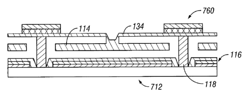
Next, in Figure 14A, a layer of insulating material 740 is deposited over the
mechanical
layer 492. In the depicted embodiment, a layer of rigid material 750 is then
deposited over the
insulating layer 740. However, as will be discussed in greater detail below,
in certain
embodiments, the layer of rigid material may not be necessary, if the layer of
insulating material
740 is sufficiently thick and/or rigid. The layer of insulating material 740
may comprise, in one
embodiment, an oxide such as silicon oxide, but any suitable material which
can serve as an
electrical insulator may be used. The layer of rigid material 750 may be any
suitable material,
and the use of an insulating layer 740 in contact with the patterned
mechanical layer 492 enables
the use of electrically conductive material in the rigid layer 750, as the
rigid layer is electrically
-21-
CA 02520376 2005-09-21
isolated from the mechanical layer. In one embodiment, the rigid layer 750
comprises the same
material used in the mechanical layer 492. In one embodiment, both the
mechanical layer 492
and the rigid layer 750 comprise nickel. In alternate embodiments, one or both
of the layers 492
and 750 may comprise aluminum. However, it may be desirable to utilize a
different material, as
the mechanical layer 492 will be formed of a material which permits flexure,
and additional
rigidity may be desired for the rigid layer 750. A wide range of materials may
be suitable for use
in the rigid layer 750, as depositing a sufficiently thick layer of these
materials may provide the
necessary rigidity.
In Figure 14B, it can be seen that the rigid layer 750 has been etched, using
the insulator
layer 740 as an etch stop. The insulator layer 740 has itself then been
etched, using the
mechanical layer 492 and the underlying sacrificial layer 462 and the remnants
of the resist layer
472 as etch stops. By these etches, cap structures 760 having a rigid layer
750 overlying an
insulating layer 740 are formed above posts 118.
Next, as seen in Figure 14C, the resist layer 472 is removed, such as by using
an ashen as
1 S discussed previously, leaving cavities 474. In Figure 14D, a release etch
is performed to remove
the sacrificial layers 462 and 452, separating the mirror layer 114 from the
flexible layer 134
above the mirror and the optical stack 116 below the mirror, thereby forming a
modulator
element 712. If the mechanical layer 492 (see Figure 14C) was previously
etched so as to totally
remove the mechanical layer from above the posts 118, a mechanical layer 492
(see Figure 14C)
forms a flexible layer 134 wherein the flexible layer is suspended from the
insulated underside of
the caps 760. This enables the creation of very thin supporting posts, as the
thickness required
for the purposes of physical support may be significantly less than the amount
of surface area
required at the top of the post to provide the necessary electrical isolation
between the various
features of the flexible layer 134. Because the caps 760 extend at least
partially over the mirrors
114, the surface area required for electrical isolation does not negatively
impact the amount of
functional area in the modulator element 712. 1n alternate embodiments, as
discussed above, the
caps 760 may be formed solely of insulating material 740, if the insulating
material has sufficient
thickness or rigidity to support the flexible layer 134.
In further embodiments, the preformed support posts may comprise a column of
conductive material such that the top of the post 118 may be placed in
electrical communication
with an element located below the post. In such a situation, upon deposition
of the insulating
layer 740, the insulating layer 740 may be etched over the support post so as
to expose the
conductive material within the post 118 without exposing the patterened
mechanical layer 492.
When the layer of rigid material 750 is deposited over the insulating layer
740, the cavity in the
insulating layer is filled, and provided the rigid material 750 is
electrically conductive, an
-22-
CA 02520376 2005-09-21
electrical connection can be made between the top of the resulting cap 760 and
an element
underlying the post I 18.
Overlying support material may be formed above the other types of support
posts
discussed in this application. For instance, a method of providing an
overlying cap structure
includes the steps depicted in Figures l0A-IOF. However, in the embodiment of
Figure 15, after
the mechanical layer 282 has been etched and the resist layer 292 (see Figure
lOF) has been
removed, a layer of insulating material 740 is deposited over the patterned
mechanical layer 282,
and a layer of rigid support material 750 is then deposited over the
insulating layer 740, as can be
seen in Figure 15A.
Moving to Figure 15B, it can be seen that cap structures 760 have been created
by
etching the rigid support layer 750, using the insulating layer 740 as an etch
stop. The insulating
layer 740 has then been etched, using the underlying mechanical layer 282 and
sacrificial layer
262 as etch stops.
Then, in Figure 15C, it can be seen that an interferometric modulator element
712 is
formed, by etching the sacrificial material 252 and 262 to release the mirror
114, as discussed
above. Thus, the interferometric modulator element 712 comprises posts 188
made from
planarization material, and an overlying cap 760, which provides additional
support for the
flexible layer 134. In alternate embodiments, the mechanical layer 282 may be
etched so as to
completely remove the mechanical layer overlying the curved upper surface of
the posts 188.
The caps 760 can then extend sufficiently beyond the edges of the post 188 to
support the flexible
layer 134.
Another method of providing additional support for support posts, such as the
support
posts 118 of Figure 8I, includes the steps of Figures 8A-8H. Once the
mechanical layer 282 has
been patterned and the resist layer 292 (see Figure 8H) has been removed, as
described with
respect to Figures 8H and 8I, an insulating layer 740 and a support layer 750
are deposited above
the patterened mechanical layer 282, as seen in Figure 16A. Next, in Figure
16B, the rigid
support layer 750 is first etched, followed by the insulator layer 740,
forming a cap structure 760
of additional support material. 1n Figure 16C, an interferometric modulator
712 is formed by
performing a release etch, removing the sacrificial layers 262 and 252,
releasing the mirror 114,
as discussed above.
Another method of forming cap structures includes forming an interferometric
modulator
comprising freestanding support posts 652 (see Figure 17F). This method
includes the process of
Figures 8A-8E. Following that process, in Figure 17A, a resist layer 640 is
deposited over the
sacrificial layer 262. However, unlike the resist mask 272 of Figure 8F, the
resist mask 640 of
Figure 17A need not have an aperture 274 for etching. Rather, the resist mask
640 need only
-23-
CA 02520376 2005-09-21
provide apertures within the post holes 260, for etching the portion of
sacrificial layer 262
exposed by the resist mask 640.
In Figure 17B, it can be seen that the resist mask has been used to etch the
sacrificial
layer 262 to expose the oxide layer 250 underneath the post hole 260 of Figure
17A. A layer of
support post material 650 is then deposited. In this embodiment, it can be
seen that the support
post material is non-planarizing, and thus the deposited layer conforms to the
shape of the
underlying layers, leaving part of the post hole 260 unfilled, rather than
filling the entirety of the
post hole. While in some embodiments the layer of support post material 650
may comprise
material suitable for use as a mechanical layer, it will be understood that
the selection of support
post material need not be so limited. Rather, the support post material 650
may advantageously
be a material which has significant rigidity, rather than the flexibility
desirable in mechanical
layer material. Additionally, the support post material 650 is desirably
selectively etchable
relative to the sacrificial layer 262.
In Figure 17C, it can be seen that the support post material 650 has been
patterned and
etched such that certain support post material beyond the vicinity of the post
holes 260 (see
Figure 17A) has been removed, leaving support posts 652. In one embodiment,
these support
posts are roughly symmetrical about a central axis, and are thus substantially
conical in shape in
the center, having a wide, substantially flat outer edge area. In another
embodiment, the support
posts may be wider in one direction than in another, and are thus
substantially wedge-shaped.
Next, in Figure 17D, a layer of insulating material 840 is deposited over the
support posts
652 and the exposed underlying sacrificial layer 262. The insulating material
840 is then
patterned and etched so as to remove certain insulating material 840 overlying
the sacrificial
material 262, leaving insulating material only in the area around the support
posts 652. An
aperture 874 is then etched in the sacrificial layer, exposing the underlying
mirror layer 254. In
Figure 17E, it can be seen that a mechanical layer 860 is then deposited, such
that it overlies the
insulating material 840 and fills the aperture 874. The mechanical layer 860
is then patterned and
etched to form features (not shown).
In Figure 17F, it can be seen that a release etch has been performed to remove
the
sacrificial material 262 and 252, separating the mirror 114 from the
surrounding material, as
discussed above. An interferometric modulator element 812 is thus formed,
having cap structures
formed from insulating material 840, which are located above posts 652 and
provide support for
the flexible layer 134. In the depicted embodiment, no additional rigid
support layer may be
necessary, as the wide underlying support post 652 may provide sufficient
rigidity.
It is to be recognized, that the order of layers and the materials forming
these layers in the
above embodiments are merely exemplary. As an example, in the method of
Figures 13A-13F,
no sacrificial layer need be deposited. Rather, the planarization layer can
serve as the entire
-24-
CA 02520376 2005-09-21
sacrificial material, which will then be removed to form the cavity between
the deformable upper
layer and the optical stack. Moreover, in some embodiments, other layers, not
shown, may be
deposited and processed to form portions of the interferometric modulator
element 112 or to form
other structures on the substrate. In other embodiments, these layers may be
formed using
alternative deposition materials, may be deposited in different order, or
composed of different
materials, as would be known to one of skill in the art, or as also discussed
in more detail in the
patents and applications discussed above.
As another example, the cap structures discussed above may be utilized in
embodiments
in which the flexible layer serves as the movable reflective layer. For
instance, the embodiment
depicted in Figure 13F may be modified to include cap structures at the top of
the support posts,
from which the flexible reflective layer is suspended. Other embodiments
having a combination
movable/reflective layer may be similarly modified to provide additional
support, improved
mechanical characteristics, and increased functional area within the display.
It is also to be recognized that, depending on the embodiment, the acts or
events of any
methods described herein can be performed in other sequences, may be added,
merged, or left out
all together (e.g., not all acts or events are necessary for the practice of
the methods), unless the
text specifically and clearly states otherwise.
While the above detailed description has shown, described, and pointed out
novel
features of the invention as applied to various embodiments, it will be
understood that various
omissions, substitutions, and changes in the form and details of the device or
process illustrated
may be made by those skilled in the art without departing from the spirit of
the invention. As will
be recognized, the present invention may be embodied within a form that does
not provide all of
the features and benefits set forth herein, as some features may be used or
practiced separately
from others.
-25-