Note: Descriptions are shown in the official language in which they were submitted.
CA 02520661 2005-09-27
WO 2004/088719 PCT/US2004/009248
NANOTUBE-ON-GATE FET STRUCTURES AND APPLICATIONS
Cross-Reference To Related Applications
[0001] This application claims priority under 35 U.S.C. ~119(e) to U.S.
Provisional Pat. Apl., Ser. No. 60/459,224, filed on March 2S, 2003, entitled
Na>zotube-O>z-Gate FET Structures and Applications, which is incorporated
herein by
reference in its entirety.
[0002] This application is related to the following U.S. applications, the
contents
of which are incorporated herein in their entirety by reference:
U.S. Provisional Apl. Ser. No. 601459,223 filed on March 2S, 2003,
entitled NRAIUI Bit Selectable Two-Device Nayzotube Az°ray; and U.S.
Pat.
Apl., Ser. No. (inserted upon USPTO desig_nation), filed on the same day
as the present application, entitled NRAM Bit Selectable Two-Device
Naz2otube Array.
U.S. Provisional Patent Application No. 60/459,253, filed on March 2~,
2003, entitled ~Sin~le Trazzsistoz° with Izztegrated Narzotube (NT
FET), acid
U.S. Pat. Apl, Ser. No. (inserted upon USPTO designation), filed on the
same day as the present application, entitled A Four Terminal Non-
volatile Transistor Device.
U.S. Provisional Patent Application No. 60/459,222, filed on March 28,
2003, entitled Norz-Volatile RCell arz.d Array usizz~ Nazaotube Switch
Positiozz for hzfof~rzatiora State, and U.S. Pat. Apl, Ser. No. (inserted upon
USPTO designation), filed on the same day as the present application,
entitled Nozz-Volatile Razu Cell and Array Usitag NazZOtube Switch 1~ositiozz
for Irrforzzzatiozz State.
Background
Technical Field
[0003] The invention relates to non-volatile transistors structures and more
specifically to non-volatile transistors using nanotube (NT) components.
2. Discussion of Related Art
[0004] Important characteristics for a memory cell in electronic device are
low
cost, nonvolatility, high density, low power, and high speed. Conventional
memory
solutions include Read Only Memory (ROM), Programmable Read only Memory
(PROM), Electrically Programmable Memory (EPROM), Electrically Erasable
CA 02520661 2005-09-27
WO 2004/088719 PCT/US2004/009248
Programmable Read Only Memory (EEPROM), Dynamic Random Access Memory
(DRAM) and Static Random Access Memory (SRAM).
[0005] ROM is relatively low cost but cannot be rewritten. PROM can be
electrically programmed but with only a single write cycle. EPROM has read
cycles
that are fast relative to ROM and PROM read cycles, but has relatively long
erase
times and reliability only over a few iterative read/write cycles. EEPROM (or
"Flash") is inexpensive, and has low power consumption but has long write
cycles
(ms) and low relative speed in comparison to DRAM or SRAM. Flash also has a
finite number of readlwrite cycles leading to low long-term reliability. ROM,
PROM,
EPROM and EEPROM are all non-volatile, meaning that if power to the memory is
interrupted the memory will retain the information stored in the memory cells.
[0006] DRAM stores charge on transistor gates that act as capacitors but must
be
electrically refreshed every few milliseconds complicating system design by
requiring
separate circuitry to "refresh" the memory contents before the capacitors
discharge.
SRAM does not need to be refreshed and is fast relative to DRAM, but has lower
density and is more expensive relative to DRAM. Both SRAM and DRAM are
volatile, meaning that if power to the memory is interrupted the memory will
lose the
information stored in the memory cells.
[0007] Consequently, existing technologies are either non-volatile but are not
randomly accessible and have low density, high cost, and limited ability to
allow
multiples writes with high reliability of the circuit's function, or they are
volatile and
complicate system design or have low density. Some emerging technologies have
attempted to address these shortcomings.
[000] For example, magnetic RAM (MRAM) or ferromagnetic RAM (FRAM)
utilizes the orientation of magnetization or a ferromagnetic region to
generate a
nonvolatile memory cell. MRAM utilizes a magnetoresistive memory element
involving the anisotropic magnetoresistance or giant magnetoresistance of
ferromagnetic materials yielding nonvolatility. Both of these types of memory
cells
have relatively high resistance and low-density. A different memory cell based
upon
magnetic tunnel junctions has also been examined but has not led to large-
scale
commercialized MRAM devices. FRAM uses a circuit architecture similar to DRAM
but which uses a thin film ferroelectric capacitor. This capacitor is
purported xo retain
2
CA 02520661 2005-09-27
WO 2004/088719 PCT/US2004/009248
its electrical polarization after an externally applied electric field is
removed yielding
a nonvolatile memory. FRAM suffers from a large memory cell size, and it is
difficult to manufacture as a large-scale integrated component. See U.S.
Patent Nos.
4,853,893; 4,888,630; 5,198,994
[0009] Another technology having non-volatile memory is phase change memory.
This technology stores information via a structural phase change in thin-film
alloys
incorporating elements such as selenium or tellurium. These alloys are
purported to
remain stable in both crystalline and amorphous states allowing the formation
of a bi-
stable switch. While the nonvolatility condition is met, this technology
appears to
suffer from slow operations, difficulty of manufacture and reliability and has
not
reached a state of commercialization. See U.S. Patent Nos. 3,448,302;
4,845,533;
4,876,667; 6,044,008.
[0010] Wire crossbar memory (MWCM) has also been proposed. See U.S. Patent
Nos. 6,128,214; 6,159,620; 6,198,655. These memory proposals envision
molecules
as bi-stable switches. Two wires (either a metal or semiconducting type) have
a layer
of molecules or molecule compounds sandwiched in between. Chemical assembly
and electrochemical o~gidation or reduction are used to generate an "on" or
"ofd' state.
This form of memory requires highly specialized wire junctions and may not
retain
non-volatility owing to the inherent instability found in redox processes.
[0011L] Recently, memory devices have been proposed which use nanoscopic
wires, such as single-walled carbon nanotubes, to form crossbar junctions to
serve as
memory cells. See W~ 01/03208, Nanoscopic Wire-Based Devices, Arrays, and
Methods of Their Manufacture; and Thomas Rueckes et al., "Carbon Nanotube-
Based
Nonvolatile Random Access Memory for Molecular Computing," Science, vol. 289,
pp. 94-97, 7 July, 2000. Hereinafter these devices are called nanotube wire
crossbar
memories (NTWCMs). Under these proposals, individual single-walled nanotube
wires suspended over other wires define memory cells. Electrical signals are
written
to one or both wires to cause them to physically attract or repel relative to
one
another. Each physical state (i.e., attracted or repelled wires) corresponds
to an
electrical state. Repelled wires are an open circuit junction. Attracted wires
are a
closed state forming a rectified junction. When electrical power is removed
from the
CA 02520661 2005-09-27
WO 2004/088719 PCT/US2004/009248
junction, the wires retain their physical (and thus electrical) state thereby
forming a
non-volatile memory cell.
[0012] The NTWCM proposals to date rely on directed growth or chemical self
assembly techniques to grow the individual nanotubes needed for the memory
cells.
These techniques are now believed to be difficult to employ at commercial
scales
using modern technology. Moreover, they may contain inherent limitations such
as
the length of the nanotubes that rnay be grown reliably using these
techniques, and it
may difficult to control the statistical variance of geometries of nanotube
wires so
grown.
[0013] The ideal memory for at least some purposes is one which would offer
low
cost per bit, high density, fast random access, readlwrite cycle times of
equal duration,
low power consumption, operation over a wide temperature range, a single low-
voltage power supply, with a high degree of radiation tolerance. The non-
volatile
described herein cell offers high speed read, but also high speed write
(nanosecond)
versus the slow (microsecond ~z millisecond) write time of EEPR~M and FLAS~l
EEPR~M type of memories. The memory is much denser than conventional SRAM
because it has a two device, NT and 3 array line structure, and offers
competitive
performance. The density is less than that of DRAM cells, however, the product
offers
NDR~ operation and non-volatility.
[001h.] U.S. Patent Publication No. 2003-002166 discloses, among ~ther things,
electromechanical circuits, such as memory cells, in which circuits include a
structure
having electrically conductive traces and supports extending from a surface of
a
substrate. Nanotube ribbons are suspended by the supports that cross the
electrically
conductive traces. Each ribbon comprises one or more nanotubes. The ribbons
are
formed from selectively removing material from a layer or matted fabric of
nanotubes.
[0015] For example, as disclosed in U.S. Patent Application Publication No.
2003-0021966, a nanofabric may be patterned into ribbons, and the ribbons can
be
used as a component to create non-volatile electromechanical memory cells. The
ribbon is electromechanically-deflectable in response to electrical stimulus
of control
traces andlor the ribbon. The deflected, physical state of the ribbon may be
made to
represent a corresponding information state. The deflected, physical state has
non-
4
CA 02520661 2005-09-27
WO 2004/088719 PCT/US2004/009248
volatile properties, meaning the ribbon retains its physical (and therefore
informational) state even if power to the memory cell is removed. As explained
in
U.S. Patent Application Publication No. 2003-0124325, three-trace
architectures may
be used for electromechanical memory cells, in which the two of the traces are
electrodes to control the deflection of the ribbon.
Sufnmary
[0016] The invention provides nanotube on gate FET structures and applications
of such, including n2 crossbars requiring only 2n control lines.
[0017] According to one aspect of the invention, a non-volatile transistor
device
includes a source region and a drain region of a first semiconductor type of
material
and a channel region of a second semiconductor type of material disposed
between
the source and drain region. A gate structure is made of at least one of
semiconductive or conductive material and is disposed over an insulator over
the
channel region. A control gate is made of at least one of semiconductive or
conductive material. An electromechanically-deflectable nanotube switching
element
is in fixed contact with one of the gate structure and the control gate
structure and is
not in fixed contact with the other of the gate structure and the control gate
structure.
The device has a network of inherent capacitances, including an inherent
capacitance
of an undeflected nanotube switching element in relation to the gate
structure. The
network is such that the nanotube switching element is deflectable into
contact with
the other of the gate structure and the control gate structure in response to
signals
being applied to the control gate and one of the source region and drain
region.
[001] According to another aspect of the invention, the nanotube switching
element is an article formed from a porous fabric of nanotubes.
[0019] According to another aspect of the invention, the fabric is
substantially a
monolayer of nanotubes.
[0020] According to another aspect of the invention, the nanotubes are single-
walled carbon nanotubes.
[0021] According to another aspect of the invention, the source and drain
regions
are disposed on or in a horizontal substrate and the nanotube switching
element is
suspended horizontally in relation to the horizontal substrate.
CA 02520661 2005-09-27
WO 2004/088719 PCT/US2004/009248
[0022] According to another aspect of the invention, the source and drain
regions
are formed as diffusions and one of the source and drain diffusions is a
selection line
for the device, and wherein the nanotube switching element is a second
selection line
for the device.
[0023] According to another aspect of the invention, the source and drain
regions
are disposed orthogonal to the nanotube element.
[0024] According to another aspect of the invention, the device has an area of
about 4F2.
[0025] According to another aspect of the invention, the device includes a
metallic layer disposed on the gate structure on a surface facing the nanotube
switching element.
[0026] According to another aspect of the invention, the nanotube switching
element is supported by supports having a known dielectric characteristic and
wherein
the geometry of the supports is of a tailored size to create a known inherent
capacitance of an undeflected nanotube switching element in relation to the
gate
structure and wherein the known inherent capacitance of the undeflected
nanotube
switching element has a known ratio relationship to an inherent capacitance
characterizing the gate structure in relation to the channel region.
[0027] According to another aspect of the invention, the ratio relationship is
about
~.25.
[002] According to another aspect of the invention, a release line is
positioned in
spaced relation to the nanotube switching element, and having a horizontal
orientation
that is parallel to the orientation of the source and drain diffusions.
[0029] According to another aspect of the invention, the device includes a
metallic layer disposed on the release line on a surface facing the nanotube
switching
element.
[0030] According to another aspect of the invention, the contact between the
nanotube switching element and the one of the control gate and gate structure
is a
non-volatile state.
[0031] According to another aspect of the invention, a crossbar array has n
input
lines and n output lines and n2 non-volatile transistor devices, each device
including a
source region and a drain region of a first semiconductor type of material, a
channel
6
CA 02520661 2005-09-27
WO 2004/088719 PCT/US2004/009248
region of a second semiconductor type of material disposed between the source
and
drain region, a gate structure made of at least one of semiconductive or
conductive
material and disposed over an insulator over the channel region, a control
gate made
of at least one of semiconductive or conductive material, an
electromechanically-
deflectable nanotube switching element wherein the element is in fixed contact
with
one of the gate structure and the control gate structure and wherein the
element is not
in fixed contact with the other of the gate structure and the control gate
structure; the
nanotube switching element being deflectable into non-volatile contact with
the other
of the gate structure and the control gate structure in response to signals
being applied
to the control gate and one of the source region and drain region, and a
release line
positioned in spaced relation to the nanotube switching element. The crossbar
also
includes a switch line decoder providing n select lines, each select line
coupled to one
of the source and drain regions of each device of a corresponding set of
devices, and a
release line decoder providing n select lines, each release line coupled to a
release line
of each device of a corresponding set of devices.
~y°i~f Desct'i~a~i~ra ~f ~h~ l~r~~~itt~
[~~~~7 In the Drawing:
Figure lA is a nanotube (NT) -on-gate of FET schematic;
Figure 1B is a nanotube (NT) -on-gate of FET schematic with a diode to
discharge node;
Figure 1C shows a NT on gate structure and a corresponding capacitance
network that can be modulated;
Figure 2 is a cross section, conceptual schematic showing the structural
location of the capacitance network of Figure 1C;
Figure 3A is a cross section, conceptual schematic showing the structural
location of the capacitance network in a certain regime;
Figure 3B is a cross section, conceptual schematic showing the structural
location of the capacitance network in another regime;
7
CA 02520661 2005-09-27
WO 2004/088719 PCT/US2004/009248
Figure 4A and 4B illustrate the write operations of the NT switch in the OFF
mode and ON mode respectively;
Figure 5 shows the top view of a non-volatile array cell according to certain
embodiments of the invention;
Figure 6A and 6B show cross sections of the cell of Figure 5 in the OFF mode
and ON mode respectively;
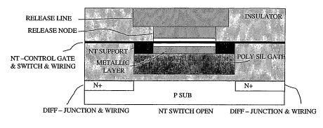
Figure 7A and 7B show cross sections of Figure 5 with a metallic layer
between the polysilicon gate and the NT control gate in the OFF mode
and ON mode respectively;
Figure 8A and 8B show cross sections of Figure 5 that illustrate vertical
structures in which the FCf is metallic line in the OFF mode and ON
mode respectively;
Figure ~ shows intermediate structures used in building the NT support
structure of Figure 7 A & B;
Figure 9A is the starting structure;
Figure 9B shows the structure after planarization by C1VIP or other means;
Figure 9C shows the metallic layer after being etched back;
Figure 91~ shows the structure after a sacrificial layer has been deposited;
and
planarized prior to the deposition of the NT ribbon;
Figure 10 illustrates a top view of a higher performance One Time
Programmable (OTP) cell;
Figure 11 illustrates a cross section of Figure 10;
Figure 12 is a cross section of Figure 10 along the NT word line;
Figure 13 illustrates four bits of an OTP array;
8
CA 02520661 2005-09-27
WO 2004/088719 PCT/US2004/009248
f'
Figure 14 illustrates the timings of the read and write-once operation;
Figure 15A, 15B and 15C illustrate the Nanotube-on-Gate FET structures
identical to lA, 1B and 1C respectively in read, release/write mode;
Figure 16 shows Figure 5 with a release line RL added above and orthogonal
to the NT patterned ribbon;
Figure 17A and 17B illustrate cross sections of Figure 16 along the nanotube
word line in the OFF mode and ON mode respectively;
Figure 18 is a schematic of four cells of an array formed using the cell
described in Figures 16, and 17A~B;
Figure 19 illustrates the timing diagram of the memory array in Figure 18;
Figure 20 is an illustration of a conventional (prior art) crossbar switch;
Figure 21 illustrates the top view of a high performance NT-on-Gate FET
device; and
Figure 22 illustrates a 4x4 crossbar switch using NT-on-Gate FET switches.
~~~~~L~~ ~e~~~~a~i~~~
[0033] The NT electromechanical switching components in the described
embodiments incorporate a nanofabric component. More specifically, preferred
embodiments provide transistor devices in which a nanotube switching element
is
integrated into a control element of the transistor, such as the gate of a FET
device.
(Nanotube switching elements are described in more detail in other
applications
and/or patents identified below, and are discussed herein to the extent
relevant for
understanding the preferred embodiments.)
[0034] Figure lA illustrates a nanotube (NT) -on-gate of FET approach. This
structure utilizes a nanofabric-based switch NT1 which controls the FET
transistor
gate which controls the transistor channel, and therefore the current through
the
transistor as shown. The gate voltage of FET1 is not defined; it floats.
Therefore if a
9
CA 02520661 2005-09-27
WO 2004/088719 PCT/US2004/009248
voltage is applied to node 1 using SELL, the voltage across nanotube NTl is
not
known.
[0035] Figure 1B changes the arrangement by adding DIODE1 between substrate
diffusion 7 and discharging node 2', allowing a leakage current to flow
between
diffusion 7 and discharging node 2,'. Node 2' will be kept at 0 volts. In
operation,
sufficient voltage applied to node 1 using SELL will cause nanotube NT1 to
switch.
Because this cell requires an additional connection in relation to the cell
shown in
Figure lA, the cell of Figure 1B is relatively large.
[0036] Figure 1C illustrates a different cell that is smaller than that shown
in
Figure 1B, and that may be operated as a memory cell or non-volatile
transistor
device. The cell is shown in a capacitance network that can be modulated in
such a
way that the voltage at node 2 is defined, and in such a way that NT1 will
switch.
The voltage at node 2 can be detected without the need for additional elements
such
as the diode of Figure 1B.
[0037] lore specifically, the device of Figure 1 C may be operated as follows.
The voltage at node 2. is controlled by a combination of the voltages applied
to node 1
and node 4~. The voltage at node 1 is applied to the capacitance network and
channel
region 3 is inverted. If the voltage at node 4 is set to zero, then electrons
remain in
the channel region, and capacitor C36 between the channel region and the
senuconductor substrate is bypassed (not in the capacitor network). In such a
case,
node 2 voltage swing is minimized, which in turn maximizes the voltage
difference
between node 1 and node ~. If the difference in voltage between nodal and node
2
exceeds the nanotube electromechanical switching threshold voltage (VNT-TH)9
then
nanotube switch NT1 closes and a conductive path is formed between node l and
node 2. If, however, the voltage at node 4 is not zero (1 to 3 volts, for
example), then
capacitors C23 and C36 are in series, the node 2 voltage swing is maximized,
which in
turn minimizes the voltage difference between node 1 and node 2. In such a
case the
nanotube electromechanical switching threshold voltage (VNT-TH) is not
exceeded, and
switch NT1 does not switch, and remains in the open position. Note that during
the
switch setting operation, node 5 may be left floating (open), but should be
grounded
for the read operation. It should be noted that Figures 1A, 1B, and 1C show
the arrow
as only closing the NT1; these figures are thus depictive of one time
programmable
CA 02520661 2005-09-27
WO 2004/088719 PCT/US2004/009248
(OTP) devices; however, the invention itself and preferred embodiments
described
below include devices allowing multiple programming.
[0038] Figure 2 is a simplified cross section of the structural location of
the
capacitance network and nodes in the schematic of the Figure 1C structure. A
nanotube NT fabric element is used as the control gate 1 of the device and is
capacitively coupled to a floating gate (FG) 2 by capacitor C12. A NT fabric
element
is used as the word line in array configurations, and as a switch that
contacts floating
gate 2 when activated. Other materials may be used as the word line under
other
embodiments of the present invention. Gate FG is referred to herein as a
floating
gate, but in reality it only floats when the NT is in the "OFF" state. In the
"ON" state,
NT contacts FG 2 with an ohmic contact, and FG is no longer floating. When NT
contacts FG, then capacitor C12 is shorted out. The capacitor between FG node
2 and
the FET channel 3 is C~3. Capacitor C36 is also referred to as the depletion
capacitor
CDEP. Capacitor C36 not part of the network when an inverted channel exists;
capacitor C36 is part of the network when there is no inverted channel.
[0039] Figures 3A-~ illustrate channel modulation using voltage VD. During a
write (program) operation, a channel region is formed by applying a control
gate
voltage that couples to the FG node by means of a capacitor network such that
the
transistor threshold voltage VTH is exceeded. The voltage of a diffusion
(either
diffusion) is modulated by applied voltage. For example, if VD = 0, electrons
stay in
the channel region, and the channel stays inverted. If VD is positive, e.g.,
between 1-3
volts, electrons are removed from the channel region which becomes depleted.
The
diffusion voltage modulates the capacitance network controlling the voltage on
the
floating gate FG (node 2 in Figures lA & 1C).
[0040] Figure 4 illustrates the write operation of the NT switch. The nature
in
which the nanotube element may be caused to deflect from one state to the
other and
the manner in which such switches may be arranged and constructed are more
fully
described in incorporated references, identified below. However, for purposes
of
describing the preferred embodiments, one can envision an electromechanical
switch.
The NT begins in the "OFF" (open) state after fabrication and can make one
"OFF"-
to-"ON" transition for OTP embodiments. Alternatively, the NT switch may be
switched to the "OFF" (open) state if released by a release node prior to
write in the
11
CA 02520661 2005-09-27
WO 2004/088719 PCT/US2004/009248
read, release/write mode of operation (discussed below). Exemplary relative
capacitance ratios are shown in Figure 4, and are as follow: C12=0.25, C23=1
and C36=
0.2.
[0041] Transistor gate capacitor C231s determined by the gate oxide thickness
and
dielectric constant (relative dielectric constant of gate oxide is typically
3.9), and the
transistor geometries, width and length, for example, as described in Baker
et. al.,
"CMOS Circuit Design, Layout, and Simulation", IEEE Press Series, 1998 pages
84
and 85. For this example, capacitor C12 is designed to be equal to 0.25 C23,
by a
choice of a control gate to FG overlap area, control gate to FG separation,
and
dielectric constant. When designing capacitor C12, the coupling area (region)
between
NT and FG includes the NT support area and the gap switching area (region) as
illustrated below. The NT support area dielectric constant depends on the
choice of
insulator support dielectric material. For example, polyimide has a relative
dielectric
constant of 2.5; silicon dioxide has relative dielectric constant of 3.9; and
alumina has
a relative dielectric constant of 9.5. The relative dielectric constant in the
gap region
is 1. The relative plate area of capacitor Cl2 may also be controlled by the
choice of
hTT fabric clamping material (insulator or conductor) above tile nanotube
fabric in the
NT support region in the perimeter of the NT fabric suspended region. For
example,
a metallic support may be used instead of an insulating support, filling-in a
controlled
portion of the porous NT fabric over tile NT support region to increase
control gate to
FG coupling area as needed. The depletion capacitance is typically 0.2 C23.
The NT
switching (select) voltage, modulated by the capacitance network, results in a
difference in voltage between NT and FG ranging from 1.0 and 2.0 volts. NT
threshold voltage should be above 1.0 volts, and below 2.0 volts; 1.5 volts,
for
example. In the "ON" state, the NT control gate is in electrical contact with
gate FG,
and the transistor threshold voltage is low, 0.3 to 0.7 volts, for example. In
the "OFF"
state, the NT control gate is not in direct electrical contact with NT, and
the control
gate voltage is coupled to the NT gate through a capacitor voltage divider
network.
Because of the voltage reduction at transistor gate NT due to the capacitor
voltage
divider, the threshold voltage for control gate formation of a channel region
between
source and drain is increased to 1.2 to 1.5 volts, for example. The effective
threshold
voltage of the transistor has been increased to 1.2 to 1.5 volts.
12
CA 02520661 2005-09-27
WO 2004/088719 PCT/US2004/009248
[0042] The stored state may be detected by applying a control gate voltage
that is
higher than the transistor "ON" state threshold voltage 0.3 to 0.7 volts, and
below the
transistor "OFF" state effective threshold voltage of 1.2 to 1.5 volts. A
control
voltage of lvolts will cause a corresponding precharged bit line voltage to
discharge
for an "ON" state, and to remain charged for an "OFF" state. A sense
amplifier/latch
may be used to detect the state of the cell. The cell may be written
(programmed)
once (OTP) and read an unlimited number of cycles.
[0043] Figure 5 is a plan view of a non-volatile array cell. The bit lines BL
are
diffusion, the word lines are patterned NT ribbons, orthogonal to the diffused
lines.
The patterned nanotube ribbons may be formed and patterned by any appropriate
method, such methods are not described herein for the sake of brevity but are
described in "Methods Of Making Carbon Nanotube Films, Layers, Fabrics,
Ribbons,
Elements And Articles," LT.S. Patent Application Serial No. 10/341005, filed
January
139 2003. The control gate is the NT in the region above the FG region. As
stated
above, the NT does not contact FG in the '6OFF" state, and therefore the FG in
this
state is truly floating. Length L and width V~ of a transistor device may be
minimum
dimensions and defined by the FG. As shown, the cell size is 4~F' ; there are
no array
contacts requiring via holes between layers of the structure.
[0044] Figures 6A-B show cross-sections of the cell taken along line A-A' of
Figure 5 and with the device in different states. The cell cross-section is
shown with
NT supports applied directly to the polysilicon gate. A release gap is shown
between
polysilicon gate and the NT film. Another release gap is above the film.
[0045] Figure 6A shows a cell in the "OFF" (open) state, i.e., the initial
state of
the cells in the OTP memory. Figure 6B shows the "ON" (closed or switched)
state
for selected bits.
[0046] Figure 7 shows a cross section of a cell like the cell shown in Figure
5 only
having a metallic layer between the polysilicon gate and the NT control gate.
The
metal layer changes the electrode material and therefore it may be used in
different
applications and may by treated differently. Polysilicon can have asperities
(spikes)
on the top surface that can locally concentrate an electric field. Any
potential
asperities are covered by the metal layer. During metal layer formation, the
metal
layer electrode surface can be planarized using well known techniques such as
13
CA 02520661 2005-09-27
WO 2004/088719 PCT/US2004/009248
chemical mechanical polishing (CMP) or reactive ion etch (RIE). Like the cells
shown in Figures 5 and 6, the cell as shown in Figure 7 also has no contacts
between
layers. As shown, this cell operates in OTP mode.
[0047] Figure 8 illustrates yet another embodiment of an OTP device according
to
certain embodiments of the present invention. This cell is like the cell shown
in
Figure 5 but this cell has a FG that is metallic. As before, there are no
contacts
between layers.
[0048] Figure 9 shows intermediate structures used in building the NT support
structure of Figures 7 A ~ B. A goal that is achieved using this method is
self
alignment of the NT support structures using a sidewall spacer applied to the
minimum dimensions DMIN (FET channel length direction) prior to implantation
of
the self aligned source and drain regions of the FET. Figure 9A is the
starting
structure having side spacers, a metallic layer over a sublayer. The structure
is
planari~ed by CMP or other appropriate means, creating the intermediate
structure
shown in Figure 9B. The metallic layer is etched back creating the
intermediate
structure shown in Figure 9C. A sacrificial layer is deposited and planari~ed
(Figure
~D) prior to the deposition of the hJT ribbon. The NT fabric layer support
illustrated
in Figure 9D is one example of a support structure adjacent to the sides of
the NT
gate. NT layer pinning structures are placed over the top and side-wall of the
nanotube fabric overlapping the support structure of Figure 9D. Figures G and
7
illustrate NT fabric support structure examples in which the NT fabric layer
support is
defined on the top layer of the FG structure. The sacrificial layer is removed
later in
the process. (Creation of such suspended nanotube fabric switches is described
in
incorporated references as stated above.)
[0049] The foregoing process sequence can also used in the fabrication of the
structure shown in Figures 7A and 7B. The sidewall process approach integrates
a
support structure self aligned to the polysilicon gate structure, and it can
be used to
achieve a 4F~' cell area.
[0050] Exemplary One-Time-Programmable cell as described and shown in
Figures 5, 6, 7, 8, and 9 are very dense. The use of diffused bit lines will
mean it is
relatively slow in operation; however the use of salicided diffusions will
reduce
diffusion resistance.
14
CA 02520661 2005-09-27
WO 2004/088719 PCT/US2004/009248
[0051] Figure 10 illustrates a plan view of an OTP cell having higher
performance
than those described above. In the illustrated structure, metallic bit lines
are used for
cell selection in order to improve memory array performance. Metallic bit
lines
contact the drains of the FET devices. Source diffusions are common and may be
stitched periodically in the array structure for higher array performance.
Likewise,
NT fabric array wiring may also be stitched periodically in the array
structure to
enhance array performance. ("Stitching" is a technique known in the art.) In
one
example of stitching, a conductor such as aluminum is patterned above a
polysilicon
word line. Via holes are provided at regular intervals interconnecting the
conductor
and polysilicon word line to reduce polysilicon word line resistance, which
enhances
the performance of DRAM, SRAM and other array structures. Because this
structure
uses contacts between layers, this cell requires additional room and the cell
is larger
than 4F2. The layout of the cell changes the orientation of the NT support
structures
relative to the orientation in Figure 5. The supports in this structure are
along the
width direction of the FET device and are shown in Figure 10. Although the NT
fabric structures of Figures 5 and 10 are shown supported on two sides, the NT
fabric
structure may be supported on all four sides. As shown, the word lines are
orthogonal
to the bit lines. Such word lines may be formed from patterned nanotube-based
fabrics.
[00~~] Figure 11 illustrates a cross section of Figure 10 taken along the
metal bit
line B-B' of Figure 10. Bit line contact to drain diffusion is shown. Also in
this
figure is a cross section of the NT word line. The NT film is the control gate
of the
FET structure. In a preferred embodiment of the present invention, the
structure is
single poly; however other appropriate material may be used. The cell is shown
in the
"OFF" (open) state. The channel region and diffusions of the device are shown.
[0053] Figure 12 illustrates a cross section of Figure 10 along the NT word
line C-
C' of Figure 10. This illustration shows polysilicon FG along the width region
of the
FET device. The FG structure is situated over thin gate oxide in the channel
region
and the FG structure also overlays a thick field oxide region causing a step
in the
oxide layer. If used, a shallow trench isolation structure (not shown) can
minimize
the polysilicon step height.
CA 02520661 2005-09-27
WO 2004/088719 PCT/US2004/009248
[0054] The cross section shown in Figure 12 illustrates how the cross section
illustrated in Figures 7A and B can be planarized using the metallic layer/NT
support
films to form a controlled gap between NT film and metallic layer on the
polysilicon
gate.
[0055] The cross section illustrated in Figure 12 further shows the NT film as
an
array wire (word line), and the control gate of the FET, and as a switch that
can close
and electrically connect NT with the metallic layer on the polysilicon gate.
[0056] Figure 13 illustrates a schematic representation of four bits of an OTP
array. A corresponding array layout may use cells as illustrated in Figure 5
or Figure
10. Cells 0, 1, and 2 are shown in the "OFF" (open) state. And as stated
earlier, all
cells of an OTP memory product are open at fabrication. In this figure, cell 3
is
shown with the NT switched to the "ON" position. This bit has been programmed
once; as an OTP cell, it cannot be reprogrammed.
[0057] Figure 14 illustrates the timing and waveforms of the various lines to
perform read and write-once operations. V~hen reading the state of the device,
a
voltage of 1.25 volts is applied to the VdLO, which is an NT ribbon; BL0 is
driven
high, e.g., 1 volt, and released. If the devise is in the "ON" state, then
V~LO (the NT0
control gate CGO) is in ohmic contact with floating gate FGO ; FGO is at 1.25
volts
and turns on the FET that has a threshold voltage of 0.7 volts, for example;
and BLO
is discharged.
[005] For a device in the "OFF" state, the FGO is capacitively coupled to NT,
and the FGO voltage is 0.25 volts; the FET remains "OFF" and BLO is not
discharged. During read, adjacent cell disturb is avoided because the voltage
between the NT and the electrode (voltage between CGO - FGO) is no greater
than 1
volt, and therefore cannot perform an unintended write operation.
[0059] When writing-once, 2.5 volts is applied to the WLO (nanotube ribbon).
If
BLO is at OV, then 2 volts appears between NT and electrode (between CGO -
FGO)
and the device goes from "OFF" to "ON". If BLO is at a positive voltage (1 to
2.5
volts, for example), then the voltage between CGO and FGO is 1 volt and does
not
switch the NT. Voltage control is as explained in reference to Figures 4A and
4B,
above.
16
CA 02520661 2005-09-27
WO 2004/088719 PCT/US2004/009248
[0060] Figures 15A-C illustrate the Nanotube-on-Gate FET structure in read,
release/write mode. This structure (including the capacitance network) is a
device
analogous to the one shown in Figure 1, except the arrow indicates switching
from
"OFF" to "ON" and "ON" to "OFF." The cells described below have a release gate
added to the NT structures. This allows the device to be rewritten multiple
times.
[0061] Figure 16 illustrates a structure like the one shown in Figure 5 with a
release line RL added above and orthogonal to the NT patterned ribbon. The
cell
illustrated in Figure 16 is a read, release/write cell. RL is shown as aligned
over the
portion of the NT film suspended between the NT supports. Even allowing for
some
misalignment of RL relative to the suspended NT region between NT supports,
the
cell is a read/write cell of minimum cell area 4F2.
[0062] Figures 17A-B illustrate a cross section of the structure shown in
Figure 16
along the nanotube word line A-A' of Figure 16. Figure 17A shows the cell in
the
"OFF" mode and Figure 17E shows the cell in the "ON" mode. The cross section
shows a release node (or release electrode) above the release gap above the NT
film.
Even allowing for some misalignment of the release node relative to the NT
suspended region, the cell area is a read/write cell of minimum cell area 4
F2. In this
case, the release line contacts the release node and alignment is not
critical.
[0063] Figure 18 is a schematic of four cells of an array formed using the NT-
on-
Gate cell described in Figures 16, and 17A and E. The memory array shown in
Figure 18 is similar to the memory array of Figure 13, except that a release
node
(electrode) coupled to a release line RLO has been added. The memory array of
Figure 18 supports read, release/write mode operation, and stores the
information in a
non-volatile state, which means the information remains unchanged when power
is
turned off. Such an array may be referred to as a nanotube random access
memory
(NRAM) array. Cells 0, 1, and 2 are illustrated in the "OFF" state, and cell 3
is
illustrated in the "ON" state. Unlike the OTP cells described above, any cell
can be
turned (written/programmed) to the "ON" state, and be returned to the "OFF"
state.
[0064] Figure 19 illustrates the timing diagram and waveforms of the memory
array in Figure 18. Read and write operation was illustrated in Figure 14 for
the OTP
array shown in Figure 13, and such operation is the same for the array shown
in
Figure 18. Release RLO timing is introduced with a release voltage pulse of
5.5 volts.
17
CA 02520661 2005-09-27
WO 2004/088719 PCT/US2004/009248
Higher voltage may require some special layout and/or junction considerations
for
peripheral array drivers; however, ideally, no junction changes are needed.
[0065] Under some embodiments of the present invention, triple-diffused
junctions can be used analogously to their current use in high voltage
circuits.
Ideally, guard ring or other layout modifications may accommodate higher
voltages if
required in the peripheral driver region. .
[0066] As shown, the RLO lines are orthogonal to the nanotube ribbon word
lines
WLO; however other layouts are possible. This specific layout accommodates
single
bit release, (byte release is described in U.S. Provisional Patent Application
No.
60/459,222). The word line voltage is at zero for devices to be released. It
is
increased to 2.5 volts to avoid writing (disturbing) an adjacent bit. The
release voltage
is the difference in voltage between RLO and WLO (RLO - WLO). For bit release
level selectivity, release voltage needs to be above 3.0 volts and less than
5.5 volts for
release operation as illustrated. (Other specific voltages are within the
scope of the
present invention; one skilled in the art will understand that the voltages
given are
merely exemplary). For byte release (~ bits simultaneously) or block release
(typically greater than 8 bits such as 2569 512, 1024, or all bits
simultaneously
released), then release voltage is any voltage between 0 and 5.5 volts. Bit or
block
release arrays, typically include bit level read ~ write.
[OOf'~] An alternative programming approach to the approach described in
Figure
19, is to set all array bit lines (BLO, BL1, and BL2 in Figure lg) to zero
volts. Then
activate array word lines (WLO and WL1 in Figure l~) to 2.5 volts, for
example, and
set all release line voltages to equal the word line voltage (such that the
word line to
release line electrostatic forces are zero), all bits are programmed to the
"ON" state.
Bits in "OFF" state switch to the "ON" state, and bits in the "ON" state
remain in the
"ON" state. Next, when selectively switching from the "ON" to the "OFF" state,
all
bit line voltages may be set at 1 to 3 volts, for example, to minimize the
risk of
switching unselected bits from the "ON" to "OFF" state. CELL 0 may then be
selectively programmed to the "OFF" state by setting word line WLO to zero
volts,
and release line RLO to release voltage to 5.5 volts, for example. To avoid
disturbing
other array cells, word line voltage is increased to 3 volts, for example, for
unselected
bit locations. This operating mode is referred to as a partial select or half
select
1~
CA 02520661 2005-09-27
WO 2004/088719 PCT/US2004/009248
mode. For RLO set at 5.5 volts, and word line WL1 set at 3 volts, CELL 2
remains in
the "ON" state. For WLO at zero volts, and RLl at 3 volts, CELL 1 remains in
the
"ON" state and for WLl at 3 volts and RLl at 3 volts, CELL 3 remains in the
"ON"
state. The illustrative example assumes the same NT threshold voltages as
illustrated
in Figure 18, and the capacitance network model described with respect to
Figures 2,
3, and 4.
[0068] Figure 20 illustrates a prior art, conventional 4-by-4 crossbar switch,
having 16 switches, as described in Mead et. al., "Introduction to VLSI
Systems",
Addison-Wesley Publishing Company, 1980, pages 157 and 158. The basic topology
of a crossbar switch dictates that any input bus bit (for example, a bit from
bus line
IBUSi) must be available at any output bus position (OBUS2, for example).
Therefore,
data paths must run at right angles to the normal bus data flow, as
illustrated in Figure
20. Note that information flow in the crossbar switch is bidirectional, so
that input
and output are interchangeable. For two buses, each n bits wide, the crossbar
switch
requires n2 connections, one to each gate of the FETs illustrated in Figure
20. For the
n = 4 bus illustrated in Figures 20, 16 bits are required, with 16 lines from
the
crossbar switch controller (decoder), one output to each of the FET s~Jitches
SW00 to
SW33. As bus width grows, the crossbar switch of Figure 20 becomes impractical
to
wire. For example, a 32 bit bus requires 1024 unique connections between
crossbar
switch controller and individual array switches. The FET switches of Figure 20
are
conventional FETs used in a pass gate configuration.
[0069] Carbon non-volatile nanotube switches use a NT-on-Gate device
structure,
and may also be used as pass gates; however, the state of the switch ("ON" or
"OFF")
may be retained when power is turned off (or lost). Also, very significantly,
NT
switches may be decoded at each switch location. Therefore, each gate is set
at the
intersection of a switch (select) line and release line, and there are n + n
(2n) array
lines required to activate each location. For a 32 bit wide bus (n = 32), the
crossbar
decoders require 64 control lines, and not 1024 lines as required for the
conventional
controller of Figure 20. The FET sources and drains are interconnected by
wires that
may be used for programming the array switches, and also transmit signals
between
bus lines.
19
CA 02520661 2005-09-27
WO 2004/088719 PCT/US2004/009248
[0070] Figure 21 illustrates a plan view of a high performance NT-on-Gate FET
device, designed as a logic switch, that forms the basis of a nanotube
crossbar switch.
The W/L ratio is typically in the 5:1 to 50:1 range. Advantages of this
structure
include high switching speed and low channel-on resistance. The presence of
metallic
terminals at the drain and source terminals of the wide device allow it to
handle
relatively large currents. The NT-on-Gate device includes the NT ribbon that
also
acts as FET control gate. The patterned NT fabric may be used as the word line
array
wiring as well as an electrostatic switching device. When used as array
wiring, the
NT fabric layer may be stitched (as is commonly done in the industry with
polysilicon
word lines, for example) with a conductor such as aluminum or copper for
higher
performance. The exemplary materials for construction of this device take
advantage
of single polysilicon technology. However, FET technologies with metal gates
may
also be used. As shown, the NT is suspended over the polysilicon gate
electrode
(metal gate electrode transistors may also be used). As drawn, the NT supports
are
along the width direction of the device (supports are shown in broken lines),
although
NT fabric supports may be used on all sides of the suspended NT fabric region.
Since
a wide device is used for performance reasons, relative switch spacing is non-
critical.
The release node RN (or release electrode) is situated above the NT ribbon,
separated
by a gap. The release line RL contacts RN, alignment, however is non-critical.
I~ey
device operational leverage is derived by the orthogonal intersection of the
release
line RL and the NT switch (select) line SL, and the capacitor network
described with
respect to Figures 2, 3, and 4, that enable crossbar switch decoder to set the
state of
each non-volatile nanotube switch using 2n array lines in lieu of n2 array
lines as
required for conventional FET switch implementations.
[0071] Figure 22 illustrates a nanotube crossbar switch with an array of 16
non-
volatile nanotube switches, and associated controllers, decoders, bus
interrupt devices,
and buses. Crossbar switches interrupt bus interconnections long enough to
change
the interconnections by re-programming the "ON"/"OFF" state of the switches.
The
nanotube crossbar switch uses the interrupt time to reset the array switches
using a
release line (RL) decoder, a combined switch line (SL) and bit line decoder,
and mode
setting transistors in series with the bus lines.
CA 02520661 2005-09-27
WO 2004/088719 PCT/US2004/009248
[0072] In operation, the NT switches are setlreset as follows. Bus
interconnection
is interrupted, and all bus line voltages in the NT switch array are set to
zero volts.
Then activate all switch lines (SLO - SL3 in Figure 22.) to switching voltage
2.5 volts,
for example, and set all release line voltages (RLO - RL3) to equal the switch
line
voltage (such that the switch line to release line electrostatic forces are
zero) -- all
NT switches are programmed to the "ON" state. NT switches in "OFF" state
switch
to the "ON" state, and NT switches in the "ON" state remain in the "ON" state.
Next,
when selectively switching from the "ON" to the "OFF" state, all bus line
voltages in
the NT switch array may be set at 1 to 3 volts, for example, to minimize the
risk of
switching unselected NT switches from the "ON" to "OFF" state. In this
example,
NT switches 1, 2, 3, and 4 remain in the "ON" position. The other 12 NT
switches in
the nanotube crossbar switch in Figure 22 are selectively switched from the
"ON"
state to the "OFF" state. By way of example, the NT switch at the intersection
of SL3
and RL2, adjacent to NT switch 1, is switched to "OFF" state as follows.
Switch line
SL3 is set to zero volts, and release line RL2 to release voltage to 5.5
volts, for
example, releasing the NT switch to the "OFF" state. To avoid disturbing other
array
NT svJitches sharing release line RL~, the voltage on select lines SLO, SL1,
and SLR. s
are increased to 3 volts, for example, for unselected NT switch locations.
This
operating mode is often referred to as a partial select or half select mode.
For RL3 set
at 5.5 volts, and select lines SLO - SL2 set at 3 volts, all other NT switches
remain in
the "ON" state. Release lines RLO, RLl, and RL3 are set at 3 volts, and all
unselected
NT switches remain undisturbed in the "ON" state. This half select NT switch
method is applied in turn, as illustrated, to all NT switches, except switches
1, 2, 3,
and 4 that remain in the "ON" state. The illustrative example assumes the NT
switches having the same threshold voltages as illustrated in Figure 18, and
the
capacitance network model described with respect to Figures 2, 3, and 4. After
all
nanotube switches are programmed, switch line SL3 is only in electrical
contact with
FG at NT switch l; switch line SL2 is only in electrical contact with FG of NT
switch
2; switch line SLl is only in electrical contact with FG of NT switch 4; and
switch
line SLO is only in electrical contact with FG of NT switch 3 of Figure 22.
Next, SL3
is set to 1.0 to 1.5, for example, and NT switch 1 forms a conductive channel
between
transistor source and drain, in order to electrically connect IBUSO and OBUS3;
SLZ is set
21
CA 02520661 2005-09-27
WO 2004/088719 PCT/US2004/009248
to 1.0 to 1.5, for example, and NT switch 2 forms a conductive channel between
transistor source and drain, in order to electrically connect IBUSI and Osusa~
SLl is set
to 1.0 to 1.5, for example, and NT switch 4 forms a conductive channel between
transistor source and drain, in order to electrically connect IBUSS and OBUSI;
SLO is set
to 1.0 to 1.5, for example, and NT switch 3 forms a conductive channel between
transistor source and drain, in order to electrically connect IBUS2 and OBUSO.
For all
other NT switches, switch line SL is coupled to FG by a capacitor voltage
divider
network, and for SL voltages of 1.0 to 1.5 volts, for example, no conductive
channel
is formed between source and drain. Next, signals T1 and T5 restore bus
interconnections. If IBUS and OBUS lines are in tristate mode during bus
interrupt, then
the transfer gates controlled by signals T1 and T5 are not needed and may be
omitted.
[0073] Table 1 compares the conventional crossbar switch requiring n2 array
connections to control the state of conventional FET switches, with the
nanotube
crossbar switch requiring 2n array connections to control the state of the NT
switches,
where n is the bus width. Therefore, the number of array lines scale linearly
with the
bus sire such that two 32 bit buses require a total of 64 array lines and
Nanotube
Orossbar Switches can be scaled to any sire bus. The conventional crossbar
switch of
Figure 20 requires 1024 individual switch array connections and is not
scalable
because of the geometric increases in the required array lines to control the
switches.
[00'4] At least some of the advantages of the Nanotube Crossbar switch
(scalability, wireability) are summarised in Table 1.
22
CA 02520661 2005-09-27
WO 2004/088719 PCT/US2004/009248
4X4 16X16 32X32 64X64
CROSSBAR CROSSBAR CROSSBAR CROSSBAR
O m z ~ z w z
O
H ~ ~ O ~ O
F- t-- -i-- t- i=- i--
z z
O W
z z z
O O z z
O O
V U
# CROSSBAR 16 16 256 256 1024 1024 4096 4096
SW ITCHES
# CROSSBAR
SWITCH 16 3 256 32 1024 64 4096 123
CONNECTIONS
Table 1
[0075] In at least some cases, the technique chosen to create a nanofabric
must
result in a sufficient quantity of nanotubes in contact with other nanotubes
which
thereby matte as a result of the nanotubes' adhesion characteristics. Certain
embodiments (e.g., memory cells) benefit when the nanofabric is very thin
(e.g., less
than 2,nm)9 for example, when the nanofabric is primarily a monolayer of
nanotubes
with sporadic overlapping (sometimes fabric will have portions that are bi-
layers or
tri-layers), or a multilayer fabric with relatively small diameter nanotubes.
Moreover,
many of these embodiments benefit when the nanotubes are single-walled
nanotubes
(SWNTs). ~ther uses of patterned nanotube ribbons (e.g., conductive traces)
may
benefit from thicker fabrics or multi-walled nanotubes (MWNTs). Still other
uses of
patterned nanotube ribbons may benefit from combinations of single-walled
nanotubes (SWNTs), and multi-walled nanotubes (MWNTs). For example, long
distance wiring traces may be selected for lower wiring impedance using MWNTs,
while local wiring and electromechanical switching regions may selected for
planarity
and electromechanical switching characteristics. The nanofabric is patterned
using
photolithographic techniques generating an electrically conductive trace of
nanotubes.
23
CA 02520661 2005-09-27
WO 2004/088719 PCT/US2004/009248
[0076] The following U.S. Patent applications disclose various methods and
techniques for making nanotube fabrics and nanotube switching elements that
may be
used as NT devices of preferred embodiments. The nanotube fabrics are porous
and
in some instances highly porous. The nanotube fabrics are substantially a
monolayer
of carbon nanotubes. In certain preferred embodiments, the carbon nanotubes
are
single-walled carbon nanotubes. Their disclosures are hereby incorporated by
reference in their entirety:
"Electromechanical Memory Array Using Nanotube Ribbons and Method
for Making Same," U.S. Patent Application Serial No. 09/915093, filed
July 25, 2001 (NAN-1);
"Electromechanical Three-Trace Junction Devices," U.S. Patent
Application Serial No. 10/033323, filed December 25, 2001 (NAN-4);
"Nanotube Films And Articles," U.S. Patent Application Serial No.
10/128115, filed April 23, 2002 (NAN-6);
"Methods ~f Making Carbon Nalzotube Films, Layers, Fabrics, Ribbons,
Elements And Articles," U.S. Patent Application Serial No. 10/341005,
filed January 13, 2003 (NAN-15);
"Devices Having Horizontally-Disposed Nanofabric Articles And
Methods Of Making The Same," U.S. Patent Application Serial No.
10/776,059, filed February 11, 2004 (NAN-19).
"Devices Having vertically-Disposed Nanofabric Articles And Methods
~f Faking "The Same," U.S. Patent Application Serial No. 10/776,572,
filed February 11, 2004 (NAN-20).
[0077] ~ther embodiments may employ double-walled nanotubes, including such
nanotubes with metallic properties.
[0078] The preferred embodiment uses electrostatic attractive forces to
deflect the
nanotube element, but other embodiments may use repulsive forces.
[0079] The invention may be embodied in other specific forms without departing
from the spirit or essential characteristics thereof. The present embodiments
are
therefore to be considered in respects as illustrative and not restrictive,
the scope of
the invention being indicated by the appended claims rather than by the
foregoing
description, and all changes which come within the meaning and range of the
equivalency of the claims are therefore intended to be embraced therein.
24
CA 02520661 2005-09-27
WO 2004/088719 PCT/US2004/009248
[0080] What is claimed is: