Note: Descriptions are shown in the official language in which they were submitted.
CA 02520992 2005-09-29
WO 2004/089048 PCT/F12004/000195
1
Method for Manufacturing an Electronic Module and an Electronic Module
The present invention relates to an electronic module and a method for
manufacturing an
electronic module.
In particular, the invention relates to an electronic module, which includes
one or more
components embedded in an installation base. The electronic module can be a
module
like a circuit board, which includes several components, which are connected
to each
other electrically, through conducting structures manufactured in the module.
The
components can be passive components, microcircuits, semiconductor components,
or
other similar components. Components that are typically connected to a circuit
board
form one group of components. Another important group of components are
components
that are typically packaged for connection to a circuit board. The electronic
modules to
which the invention relates can, of course, also include other types of
components.
The installation base can be of a type similar to the bases that are generally
used in the
electronics industry as installation bases for electrical components. The task
of the base is
to provide components with a mechanical attachment base and the necessary
electrical
connections to both components that are on the base and those that are outside
the base.
The installation base can be a circuit board, in which case the construction
and method to
which the invention relates are closely related to the manufacturing
technology of circuit
boards. The installation base may also be some other base, for example, a base
used in
the packaging of a component or components, or a base for an entire functional
module.
The manufacturing techniques used for circuit boards differ from those used
for
microcircuits in, among other things, the fact that the installation base in
microcircuit
manufacturing techniques, i.e. the substrate, is of a semiconductor material,
whereas the
base material of an installation base for circuit boards is some form of
insulating
material. The manufacturing techniques for microcircuits are also typically
considerably
more expensive that the manufacturing techniques for circuit boards.
The constructions and manufacturing techniques for the cases and packages of
components, and particularly semiconductor components differ from the
construction and
CA 02520992 2005-09-29
WO 2004/089048 PCT/F12004/000195
2
manufacture of circuit boards, in that component packaging is primarily
intended to form
a casing around the component, which will protect the component mechanically
and
facilitate the handling of the component. On the surface of the component,
there are
connector parts, typically protrusions, which allow the packaged component to
be easily
set in the correct position on the circuit board and the desired connections
to be made to
it. In addition, inside the component case, there are conductors, which
connect the
connector parts outside the case to connection zones on the surface of the
actual
component, and through which the component can be connected as desired to its
surroundings.
However, component cases manufactured using conventional technology demand a
considerable amount of space. As electronic devices have grown smaller, there
has been
a trend to eliminate component cases, which take up space, are not essential,
and create
unnecessary costs. Various constructions and methods have been developed to
solve this
problem.
One known solution is flip-chip (FC) technology, in which non-packaged
semiconductor
components are installed and connected directly to the surface of the circuit
board.
However, flip-chip technology has many weaknesses and difficulties. For
example, the
reliability of the connections can be a problem, especially in applications,
in which
mechanical stresses arise between the circuit board and the semiconductor
component. In
an attempt to avoid mechanical stresses, a suitable elastic underfill, which
equalizes
mechanical stresses, is added between the semiconductor component and the
circuit
board. This procedural stage slows down the manufacturing process and
increases costs.
Even the thermal expansion caused by the normal operation of a device may
cause
mechanical stresses large enough to compromise the long-term reliability of an
FC
structure.
US patent publication 4 246 595 discloses one solution, in which recesses are
formed in
the installation base for the components. The bottoms of the recesses are
bordered by a
two-layered insulation layer, in which holes are made for the connections of
the
component. The layer of the insulation layer that lies against the components
is made of
an adhesive. After this, the components are embedded in the recesses with
their
CA 02520992 2012-02-23
3
connection zones facing the bottom of the recess, electrical contacts being
formed to the
components through the holes in the insulation layer. If it is wished to make
the structure
mechanically durable, the component must also be attached to an installation
base, so
that the method is quite complicated. It is extremely difficult to use a
complicated
method, which demands several different materials and process stages, to
profitably
manufacture cheap products. In other ways too, the method does not correspond
to the
technology used nowadays (the patent dates from 1981).
JP application publication 2001-53 447 discloses a second solution, in which a
recess is
made for the component in an installation base. The component is placed in the
recess,
with the component's contact zones facing towards the surface of the
installation base.
Next, an insulation layer is made on the surface of the installation base and
over the
component. Contact openings for the component are made in the insulation layer
and
electrical contacts are made to the component, through the contact openings.
In this
method, considerable accuracy is demanded in manufacturing the recess and
setting the
component in the recess, so that the component will be correctly positioned,
to ensure the
success of the feed-throughs, relative to the width and thickness of the
installation board
The invention is intended to create a relatively simple and economical method
for
manufacturing electronic modules, with the aid of which a mechanically durable
construction can be achieved.
The invention is based on the component being glued to the surface of a
conductive
layer, from which conductive layer conductive patterns are later formed. After
the gluing
of the component, an insulating-material layer, which surrounds the component
attached
to the conductive layer, is formed on, or attached to the surface of the
conductive layer.
After the gluing of the component, feed-throughs are also made, through which
electrical
contacts can be formed between the conductive layer and the conductive zones
of the
component. After this, conductive patterns are formed from the conductive
layer, to
which the component is glued.
CA 02520992 2012-02-23
3a
In accordance with one aspect of the present invetnion, there is provided a
method for manufacturing an electronic module, the method comprising: -
providing
a conductive layer comprising a first surface, - providing a component
comprising a
contact surface, the contact surface comprising contact zones, - gluing the
contact
surface of the component onto the first surface of the conductive layer
through an
adhesive layer, - placing an insulating-material layer with preformed recesses
surrounding the glued component onto the first surface of the conductive
layer,
- producing feed-throughs connecting the contact zones of the component
electrically
to the conductive layer, and - producing a conductive pattern from the
conductive
layer, - wherein the step of producing feed-throughs comprises producing an
electrical contact area of conductive material formations between the
conductive
pattern and the contact zones, - wherein the step of producing the conductive
patterm
from the conductive layer comprises removing part of the conductive layer with
remaining material being the conductive pattern and the conductive material
formations penetrating the adhesive layer.
In accordance with another aspect of the present invention, there is provided
an electronic module, the module comprising: - an insulating-material layer,
which
has a first surface and a second surface; - at least one hole or recess in the
insulating-
material layer, which opens out onto the first surface; - at least one
component inside
the at least one hole or recess, wherein the component includes contact zones
on the
side of the component that faces the first surface of the insulating-material
layer, and
further wherein the component is positioned in such a way that the contact
zones are
located at a specified distance from the level of the first surface of the
insulating-
material layer; - a conductive-pattern layer, which runs on the first surface
of the
insulating-material layer and extends on top of the at least one hole or
recess in the
insulating-material layer and at the location of the contact zones of the
components;
- a hardened adhesive layer in the hole or recess in the insulating-material
layer,
between the component and the conductive-pattern layer; and - an electrical
contact
area between the conductive-pattern layer and the contact zones of the
component,
where said contact area is formed by conductive-material formations
penetrating the
adhesive layer.
CA 02520992 2012-02-23
4
Considerable advantages are gained with the aid of the invention. This because
it is
possible, with the aid of the invention, to manufacture mechanically durable
electronic
modules, which include unpackaged components embedded in an installation base.
The invention permits a quite simple manufacturing method, in which relatively
few
different materials are requited. For this reason, the invention has
embodiments, with the
aid of which electronic modules can be manufactured at low cost. For example,
in the
technique disclosed in US patent publication 4 246 595, (the references are to
figure 8 of
the patent) a support layer 24, an insulating layer 16, and an adhesion layer
17 are
required. In addition, a fourth insulating material (not shown in the
embodiment of figure
8), i.e. filler with the aid of which the component is attached to the support
layer 24, is
also required, in order to create a mechanically sturdy attachment. In the
solution of the
JP application publication 2001-53 447 too, a corresponding attachment that
entirely
surrounds the component requires about 3 - 4 separate insulating materials, or
insulating
layers (publication figures 2 and 4).
Unlike the reference publications, our invention has embodiments, in which the
component can be entirely surrounded using 2 - 3 insulating materials, or
insulating
layers. This because the contact surface of the component is glued to a
conductive layer,
so that, in preferred embodiments, the adhesive attaches the component
essentially over
the entire area of its contact surface. Elsewhere, in such an embodiment, the
component
is attached with the aid of an insulating-material layer, which acts as the
base material for
the electronic module being formed. The insulating-material layer is formed
after the
gluing of the component, so that in preferred embodiments it can be made
around the
component to conform to the shape of the component. In such embodiments, it is
possible to achieve a comprehensive attachment of the component with the aid
of an
adhesive layer and a base-material layer formed from 1 - 2 insulating-material
sheets.
In the embodiments of the invention, it is thus possible to manufacture a
circuit board,
CA 02520992 2005-09-29
WO 2004/089048 PCT/F12004/000195
inside which components are embedded. The invention also has embodiments, with
the
aid of which a small and reliable component package can be manufactured around
a
component, as part of the circuit board. In such an embodiment, the
manufacturing
process is simpler and cheaper than manufacturing methods in which separate
packaged
5 components are installed and connected to the surface of the circuit board.
The
manufacturing method can also be applied to use the method to manufacture Reel-
to-
Reel products. Thin and cheap circuit-board products containing components can
be
made by using the methods according to the preferred embodiments.
The invention also permits many other preferred embodiments, which can be used
to
obtain significant additional advantages. With the aid of such embodiments, a
component's packaging stage, the circuit board's manufacturing stage, and the
assembly
and connecting stage of the components, for example, can be combined to form a
single
totality. The combination of the separate process stages brings significant
logistical
advantages and permits the manufacture of small and reliable electronic
modules. A
further additional advantage is that such an electronic-module manufacturing
method can
mostly utilize known circuit-board manufacturing and assembly techniques.
The composite process according to the embodiment referred to above is, as a
totality,
simpler than manufacturing a circuit board and attaching a component to the
circuit
board using, for example, the flip-chip technique. By using such preferred
embodiments,
the following advantages are obtained, compared to other manufacturing
methods:
-Soldering is not needed in the connections of the components, instead an
electrical connection between the connection zones on the surface of the
component and the metal film of the installation base is created by a via-
method.
This means that the connection of a component does not need metal being
maintained molten for a long time with its associated high temperature. Thus,
the
construction is made more reliable than soldered connections. The brittleness
of
the metal alloys creates large problems particularly in small connections. In
a
solderless solution according to a preferred embodiment, it is possible to
achieve
clearly smaller constructions than in soldered solutions.
CA 02520992 2005-09-29
WO 2004/089048 PCT/F12004/000195
6
-As smaller structures can be manufactured using the method, the components
can be placed closer together. Thus, the conductors between the components
also
become shorter and the characteristics of the electronic circuits improve. For
example, losses, interferences, and transit-time delays can be significantly
reduced.
-The method permits a lead-free manufacturing process, which is
environmentally
friendly.
-When using a solderless manufacturing process, fewer undesirable
intermetallics
also arise, thus improving the long-term reliability of the construction.
-The method also permits three-dimensional structures to be manufactured, as
the
installation bases and the components embedded in them can be stacked on top
of
each other.
The invention also permits other preferred embodiments. For instance, flexible
circuit
boards can be used in connection with the invention. Further, in embodiments,
in which
the temperature of the installation base can be kept low during the entire
process, organic
manufacturing materials can be used comprehensively.
With the aid of embodiments, it is also possible to manufacture extremely thin
structures,
in which, despite the thinness of the structure, the components are entirely
protected
inside their installation base, such as a circuit board.
In embodiments, in which the components are located entirely inside the
installation
base, the connections between the circuit board and the components will be
mechanically
durable and reliable.
The embodiments also permit the design of electronic-module manufacturing
processes
requiring relatively few process stages. Embodiments with fewer process stages
correspondingly also require fewer process devices and various manufacturing
methods.
With the aid of such embodiments, it is also possible in many cases to cut
manufacturing
CA 02520992 2005-09-29
WO 2004/089048 PCT/F12004/000195
7
costs compared to more complicated processes.
The number of conductive-pattern layers of the electronic module can also be
chosen
according to the embodiment. For example, there can be one or two conductive-
pattern
layers. Additional conductive-pattern layers can be manufactured on top of
these, in the
manner known in the circuit-board industry. A total module can thus
incorporate, for
example, three, four, or five conductive-pattern layers. The very simplest
embodiments
have only one conductive-pattern layer and indeed one conductor layer. In some
embodiments, each of the conductor layers contained in the electronic module
can be
exploited when forming conductive patterns.
In embodiments, in which the conductor layer connected to a component is
patterned
only after the connection of the component, the conductor layer can include
conductor
patterns even at the location of the component. A corresponding advantage can
also be
achieved in embodiments, in which the electronic module is equipped with a
second
conductive-pattern layer, which is located on the opposite surface of the base
material of
the module (on the opposite surface of the insulation material layer relative
to the
conductive-pattern layer connected to the component). The second conductor
layer can
thus also include conductive patterns at the location of the component. The
placing of
conductive patterns in the conductor layers at the location of the component
will permit a
more efficient use of space in the module and a denser structure.
In the following, the invention is examined with the aid of examples and with
reference
to the accompanying drawings.
Figures 1 - 10 show a series of cross-sections of some examples of
manufacturing
methods according to the invention and schematic cross-sectional diagrams of
some
electronic modules according to the invention.
Figure 11 shows a cross-sectional view of one electronic module according to
the
invention, which includes several installation bases on top of each other.
In the methods of the examples, manufacturing starts from a conductive layer
4, which
CA 02520992 2005-09-29
WO 2004/089048 PCT/F12004/000195
8
can be, for example, a metal layer. One suitable manufacturing material for
the
conductive layer 4 is copper film (Cu). If the conductive film 4 selected for
the process is
very thin, or the conductive film is not mechanically durable for other
reasons, it is
recommended that the conductive film 4 be supported with the aid of a support
layer 12.
This procedure can be used, for example, in such a way that the process is
started from
the manufacture of the support layer 12. This support layer 12 can, for
example, an
electrically conductive material, such as aluminium (Al), steel, or copper, or
an insulating
material, such as a polymer. An unpatterned conductive layer 4 can be made on
the
second surface of the support layer 4, for example, by using some
manufacturing method
well known in the circuit-board industry. The conductive layer can be
manufactured, for
example, by laminating a copper film (Cu) on the surface of the support layer
12.
Alternatively, it is possible to proceed by making the support layer 12 on the
surface of
the conductive layer 4. The conductive film 4 can also be a surfaced metal
film, or some
other film including several layers, or several materials.
Later in the process, conductive patterns are made from the conductive layer
4. The
conductive patterns must then be aligned relative to the components 6. The
alignment is
most easily performed with the aid of suitable alignment marks, at least some
of which
can be made already in this stage of the process. Several different methods
are available
for creating the actual alignment marks. One possible method is to make small
through-
holes 3 in the conductive layer 4, in the vicinity of the installation areas
of the
components 6. The same through-holes 3 can also be used to align the
components 6 and
the insulating-material layer 1. There should preferably be at least two
through-holes 3,
for the alignment to be carried out accurately.
The components 6 are attached to the surface of the insulating layer 4 with
the aid of an
adhesive. For gluing, an adhesive layer 5 is spread on the attachment surface
of the
conductive layer 4, or on the attachment surface of the component 6, or on
both. After
this, the components 6 can be aligned to the positions planned for the
components 6, with
the aid of alignment holes 3, or other alignment marks. Alternatively, it is
possible to
proceed by first gluing the components to the conductive layer 4, positioned
relative to
each other, and after this making the alignment marks aligned relative to the
components.
The term attachment surface of the component 6 refers to that surface, which
faces the
CA 02520992 2005-09-29
WO 2004/089048 PCT/F12004/000195
9
conductive layer 4. The attachment surface of the component 6 includes the
contact
zones, by means of which an electrical contact can be formed with the
component. Thus,
the contact zones can be, for example, flat areas on the surface of the
component 6, or
more usually contact protrusions protruding from the surface of the component
6. There
are generally at least two contact zones or protrusions in the component 6. In
complex
microcircuits, there can be a greater number of contact zones.
In many embodiments, it is preferable to spread so much adhesive on the
attachment
surface, or attachment surfaces, that the adhesive entirely fills the space
remaining
between the components 6 and the conductive layer 4. A separate filler is then
not
required. The filling of the space between the components 6 and the conductive
layer 4
reinforces the mechanical connection between the component 6 and the
conductive layer
4, thus achieving a structure that is mechanically more durable. The
comprehensive and
unbroken adhesive layer also supports the conductive patterns 14 to be formed
later from
the conducting layer 4 and protects the structure during later process stages.
The term adhesive refers to a material, by means of which the components can
be
attached to the conductive layer. One property of the adhesive is that the
adhesive can be
spread on the surface of the conductive layer, and/or of the component in a
relatively
fluid form, or otherwise in a form that will conform to the shape of the
surface. Another
property of the adhesive is that, after spreading, the adhesive hardens, or
can be
hardened, at least partly, so that the adhesive will be able to hold the
component in place
(relative to the conductive layer), at least until the component is secured to
the structure
in some other manner. A third property of the adhesive is its adhesive
ability, i.e. its
ability to stick to the surface being glued.
The term gluing refers to the attachment of the component and conductive layer
to each
other with the aid of an adhesive. Thus, in gluing, an adhesive is brought
between the
component and the conductive layer and the component is placed in a suitable
position
relative to the conductive layer, in which the adhesive is in contact with the
component
and the conductive layer and at least partly fills the space between the
component and the
conductive layer. After this, the adhesive is allowed (at least partly) to
harden, or the
adhesive is actively hardened (at least partly), so that the component sticks
to the
CA 02520992 2005-09-29
WO 2004/089048 PCT/F12004/000195
conductive layer with the aid of the adhesive. In some embodiments, the
contact
protrusions of the component may, during gluing, extend through the adhesive
layer to
make contact with the conductive layer.
5 The adhesive used in the embodiments is typically a thermally hardening
epoxy, for
example an NCA (non-conductive adhesive). The adhesive is selected to ensure
that the
adhesive used will have sufficient adhesion to the conductive film, the
circuit board, and
the component. One preferred property of the adhesive is a suitable
coefficient of thermal
expansion, so that the thermal expansion of the adhesive will not differ too
greatly from
10 the thermal expansion of the surrounding material during the process. The
adhesive
selected should also preferably have a short hardening time, preferably of a
few seconds
at most. Within this time, the adhesive should harden at least partly, to such
an extent
that the adhesive is able to hold the component in position. Final hardening
can take
clearly more time and the final hardening can be planned to take place in
connection with
later process stages. The adhesive should also withstand the process
temperatures used,
for example, heating to a temperature in the range 100 - 265 C a few times,
and other
stresses in the manufacturing process, for example, chemical and mechanical
stress. The
electrical conductivity of the adhesive is preferably in the same order as
that of the
insulating materials.
A suitable insulating-material layer 1 is selected as the base material of the
electronic
module, for example, the circuit board. Using a suitable method, recesses, or
through-
holes are made in the insulating-material layer 1, according to the size and
mutual
positions of the components 6 to be attached to the conductive layer 4. The
recesses or
through-holes can also be made to be slightly larger than the components 6, in
which
case the alignment of the insulating layer 1 relative to the conductive layer
4 will not be
so critical. If an insulating-material layer 1, in which through-holes are
made for the
components 6, is used in the process, certain advantages can be achieved by
using, in
addition, a separate insulating-material layer 11, in which holes are not
made. Such an
insulating-material layer 11 can be located on top of the insulating-material
layer 1 to
cover the through-holes made for the components.
If it is desired to make a second conductive layer in the electronic module,
this can be
CA 02520992 2005-09-29
WO 2004/089048 PCT/F12004/000195
11
made, for example, on the surface of the insulating-material layer 1. In
embodiments, in
which a second conductive layer 11 is used, the conductive layer can be made
on the
surface of this second conductive layer 11. If desired, conductive patterns 19
can be
made from a second conductive layer 9. The conductive layer 9 can be made, for
example, in a corresponding manner to the conductive film 4. The manufacture
of a
second conductive film 9 is not, however, necessary in simple embodiments and
when
manufacturing simple electronic modules. A second conductive film 9 can,
however, be
exploited in many ways, such as additional space for conductive patterns and
to protect
the components 6 and the entire module against electromagnetic radiation (EMC
shielding). With the aid of a second conductive film 9 the structure can be
reinforced and
warping of the installation base, for example, can be reduced.
Feed-throughs, through which electrical contacts can be formed between the
contact
zones of the components 6 and the conductive layer 4, are made in the
electronic module.
Holes 17 are made in the conductive layer 4 for the feed-throughs, at the
positions of the
contact zones (in the figures, the contact protrusions 7) of the components 6.
Holes 3, or
other available alignment marks can be utilized in the alignment. The holes 17
are made
in such a way that they also penetrate through the adhesive layer that has
been left on top
of the contact zones, or contact protrusions 7. The holes 17 thus extend to
the material of
the contact protrusions 7 or other contact zones. The holes 17 can be made,
for example,
by drilling with a laser device, or by using some other suitable method. After
this,
conductive material is introduced to the hole 17, so that an electrical
contact is formed
between the components 6 and the conductive layer 4.
The manufacturing processes according to the examples can be implemented using
manufacturing methods, which are generally known to those versed in the art of
manufacturing circuit boards.
In the following, the stages of the method shown in Figures 1 - 8 are examined
in greater
detail.
Stage A (Figurel):
CA 02520992 2005-09-29
WO 2004/089048 PCT/F12004/000195
12
In stage A, a suitable conductive layer 4 is selected as the initial material
of the process.
A layered sheet, in which the conductive layer 4 is located on the surface of
a support
base 12, can also be selected as the initial material. The layered sheet can
be
manufactured, for example, in such a way that a suitable support base 12 is
taken for
processing, and a suitable conductive film for forming the conductive layer 4
is attached
to the surface of this support base 12.
The support base 12 can be made of, for example, an electrically conductive
material,
such as aluminium (Al), or an insulating material, such as polymer. The
conductive layer
4 can be formed, for example, by attaching a thin metal film to the second
surface of the
support base 12, for example, by laminating it from copper (Cu). The metal
film can be
attached to the support base, for example, using an adhesive layer, which is
spread on the
surface of the support base 12 or metal film prior to the lamination of the
metal layer. At
this stage, there need not be any patterns in the metal film.
In the example of Figure 1, holes 3 are made penetrating the support base 12
and the
conductive layer 4, for alignment during the installation and connection of
the
components 6. Two through-holes 3, for example, can be manufactured for each
component 6 to be installed. The holes 3 can be made using some suitable
method, for
example, mechanically by milling, impact, drilling, or with the aid of a
laser. However, it
is not essential to make through-holes 3, instead some other suitable
alignment markings
can be used to align the components. In the embodiment shown in Figure 1, the
through-
holes 3 used to align the components extend through both the support base 12
and the
conductive film 4. This has the advantage that the same alignment marks
(through-holes
3) can be used for aligning on both sides of the installation base.
Stage A can also be performed in the same way in embodiments in which a self-
supporting conductive layer 4 is used and from which thus totally lacks a
support layer
12.
Stage B (Figure 2):
In stage B, an adhesive layer 5 is spread on those areas of the conductive
layer 4, to
CA 02520992 2005-09-29
WO 2004/089048 PCT/F12004/000195
13
which the components 6 will be attached. These areas can be termed attachment
areas.
The adhesive layers 5 can be aligned, for example, with the aid of the through-
holes 3.
The thickness of the adhesive layer is selected so that the adhesive suitably
fills the space
between the component 6 and the conductive layer 4, when the component 6 is
pressed
onto the adhesive layer 5. If the component 6 includes contact protrusions 7,
it would be
good for the thickness of the adhesive layer 5 to be greater, for example
about 1.5 - 10
times, the height of the contact protrusions 7, so that the space between the
component 6
and the conductive layer 4 will be properly filled. The surface area of the
adhesive layer
5 formed for the component 6 can also be slightly larger than the
corresponding surface
area of the component 6, which will also help to avoid the risk of inadequate
filling.
Stage B can be modified in such a way that the adhesive layer 5 is spread on
the
attachment surfaces of the components 6, instead of on the attachment areas of
the
conductive layer 4. This can be carried out, for example, by dipping the
component in
adhesive, prior to setting it in place in electronic module. It is also
possible to proceed by
spreading the adhesive on both the attachment areas of the conductive layer 4
and on the
attachment surfaces of the components 6.
The adhesive being used is thus a electrical insulator, so that electrical
contacts are not
formed in the actual adhesive layer 5, between the contact zones (contact
protrusions 7 in
the example) of the component 6.
Stage C (Figure 3):
In stage C, the component 6 is set in place in the electronic module. This can
be done, for
example, by pressing the components 6 into the adhesive layer 5, with the aid
of an
assembly machine. In the assembly stage, the through-holes 3 made for
alignment, or
other available alignment marks, are used to align the components 6.
The components 6 can be glued individually, or in suitable groups. The typical
procedure
is for the conductive layer, which can be termed the bottom of the
installation base, to be
brought to a suitable position relative to the assembly machine, and after
this the
component 6 is aligned and pressed onto the bottom of the installation base,
which is
CA 02520992 2005-09-29
WO 2004/089048 PCT/F12004/000195
14
held stationary during the aligning and attaching.
Stage D (Figure 4):
In stage D, an insulating-material layer 1, in which there are pre-formed
recesses 2 or
recesses for the components 6 to be glued to the conductive layer 4, is placed
on top of
the conductive layer 4. The insulating-material layer 1 can be made from a
suitable
polymer base, in which recesses or cavities according to the size and position
of the
components 6 are made using some suitable method. The polymer made can be, for
example, a pre-preg base known and widely used in the circuit-board industry,
which is
made from a glass-fibre mat and so-called b-state epoxy. It is best to perform
stage D
only once the adhesive layer 5 has been hardened, or it has otherwise hardened
sufficiently for the components 6 to remain in place during the placing of the
insulating-
material layer 1.
When manufacturing a very simple electronic module, the insulating-material
layer 1 can
be attached to the conductive layer 4 in connection with stage D and the
process
continued with the patterning of the conductive layer 4.
Stage E (Figure 5):
In stage E, an unpatterned insulating-material layer 11 is placed on top of
the insulating-
material layer 1 and on top of it a conductive layer 9. Like the insulating-
material layer 1,
the insulating-material layer 11 can be made from a suitable polymer film, for
example,
the aforesaid pre-preg base. The conductive layer 9 can, in turn, be, for
example, a
copper film, or some other film suitable for the purpose.
Stage F (Figure 6):
In stage F, the layers 1, 11, and 9 are pressed with the aid of heat and
pressure in such a
way that the polymer (in the layers 1 and 11) forms a unified and tight layer
between the
conductive layer 4 and 9 around the components 6. The use of this procedure
makes the
second conductive layer 9 quite smooth and even.
CA 02520992 2005-09-29
WO 2004/089048 PCT/F12004/000195
When manufacturing simple electronic modules and those including a single
conductive-
pattern layer 14, stage E can even be totally omitted, or the layers 1 and 11
can be
laminated to the construction, without a conductive layer 9.
5
Stage G (Figure 7):
In stage G, the support base 12 is detached or otherwise removed from the
construction.
Removal can take place, for example, mechanically or by etching. Stage G can
naturally
10 be omitted from embodiments that do not employ a support base 12.
Stage H (Figure 8):
In stage H, holes 17 are made for the feed-throughs. The holes 17 are made
through the
15 conductive layer 4 and the adhesive layer 5, in such a way that the
material of the contact
protrusions 7, or other contact zones of the components 6 is exposed. The
holes 17 can be
made, for example, by drilling with a laser. The holes 17 can be aligned, for
example,
with the aid of holes 3.
Stage I (Figure 9):
In stage I, conductive material 18 is grown into the holes 17 made in stage H.
In the
example process, the conductive material is grown at the same time also
elsewhere on
top of the base, so that the thickness of the conductive layers 4 and 9 also
increases.
The conductive material 18 being grown can be, for example, copper, or some
other
sufficiently electrically conductive material. The choice of conductive
material 18 should
take into account the ability of the material to form an electrical contact
with the contact
protrusions 7 of the component 6. In one example process, the conductive
material is
mainly copper. Copper-metallizing can be performed by surfacing the holes 17
with a
thin layer of chemical copper and then continuing the surfacing using an
electrochemical
copper-growing method. Chemical copper is used, for example, because it also
forms a
surface on top of the adhesive and acts as an electrical conductor in
electrochemical
CA 02520992 2005-09-29
WO 2004/089048 PCT/F12004/000195
16
surfacing. The growth of the metal can thus be performed using a wet-chemical
method,
in which case the growing will be cheap.
In the example process, the holes 17 of the feed-throughs are first cleaned
using a three-
stage desmear treatment. After this, the feed-throughs are metallized in such
a way that
an SnPd coating catalysing the polymer is first formed, after which a thin
layer (about 2
gm) is deposited on the surface. The thickness of the copper is increased
using
electrochemical deposition.
Stage I is intended to form an electrical contact between the component 6 and
the
conductive layer 4. In stage I, it is therefore not essential to increase the
thickness of the
conductive layers 4 and 9, instead the process can equally well be planned in
such a way
that in stage I the holes 17 are only filled with a suitable material. The
conductive layer
18 can be made, for example, by filling the holes 17 with an electrically
conductive
paste, or by using some other metallizing method suitable for micro-vias.
In the later figures, the conductive layer 18 is shown with the conductive
layers 4 and 9
merged.
Stage J (Figure 10):
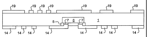
In stage J, the desired conductive patterns 14 and 19 are formed from the
conductive
layers 4 and 9 on the surface of the base. If only a single conductive layer 4
is used in the
embodiment, the patterns are formed on only one side of the base. It is also
possible to
proceed in such a way that the conductive patterns are only formed from the
conductive
layer 4, even though a second layer 9 is also used in the embodiment. In such
an
embodiment, the unpatterned conductive layer 9 can act, for example, as a
mechanically
supporting or protective layer of the electronic module, or as a protection
against
electromagnetic radiation.
The conductive patterns 14 can be made, for instance, by removing the
conductive
material of the conductive layer 4 from outside of the conductive patterns.
The
conductive material can be removed, for example, using one of the patterning
and
CA 02520992 2005-09-29
WO 2004/089048 PCT/F12004/000195
17
etching methods that are widely used and well known in the circuit-board
industry.
After stage J, the electronic module includes a component 6, or several
components 6 and
conductive patterns 14 and 19 (in some embodiments only conductive patterns
14), with
the aid of which the component or components 6 can be connected to an external
circuit,
or to each other. The conditions for manufacturing a functional totality then
exist already.
The process can thus be designed in such a way that the electronic module is
already
finished after stage J and figure 10 shows one example of a possible
electronic module
that can be manufactured using the example methods. If it is wished, the
process can also
continue after stage J, for example, by surfacing the electronic module with a
protective
substance, or by making additional conductive patterns on the first and/or
second surface
of the electronic module.
Figure 11
Figure 11 shows a multi-layered electronic module, which includes three bases
1
laminated on top of each other, together with their components 6, and a total
of six
conductive-pattern layers 14 and 19. The bases 1 are attached to each other
with the aid
of intermediate layers 32. The intermediate layer 32 can be, for example, a
pre-preg
epoxy layer, which is laminated between the installation bases 1. After this,
holes.
running through the module are drilled in the electronic module, in order to
form
contacts. The contacts are formed with the aid of a conductive layer 31 grown
in the
holes. With the aid of the conducts 31 running through the electronic module,
the various
conductive-pattern layers 14 and 19 of the installation bases 1 can be
suitably connected
to each other, thus forniing a multi-layered functioning totality.
On the basis of the example of Figure 11, it is clear that the method can also
be used to
manufacture many different kinds of three-dimensional circuit structures. The
method
can be used, for example, in such a way that several memory circuits are
placed on top of
each other, thus forming a package containing several memory circuits, in
which the
memory circuits are connected to each other to form a single functional
totality. Such
packages can be termed three-dimensional multichip modules. In modules of this
kind,
the chips can be selected freely and the contacts between the various chips
can be easily
CA 02520992 2005-09-29
WO 2004/089048 PCT/F12004/000195
18
manufactured according to the selected circuits.
The sub-modules (bases 1 with their components 6 and conductors 14 and 19) of
a multi-
layered electronic module can be manufactured, for example, using one of the
electronic-
module manufacturing methods described above. Some of the sub-modules to be
connection to the layered construction can, of course, be quite as easily
manufactured
using some other method suitable for the purpose.
The examples of Figures 1 - 11 show some possible processes, with the aid of
which our
invention can be exploited. Our invention is not, however, restricted to only
the processes
disclosed above, but instead the invention also encompasses various other
processes and
their end products, taking into account the full scope of the Claims and the
interpretation
of their equivalences. The invention is also not restricted to only the
constructions and
method described by the examples, it being instead obvious to one versed in
the art that
various applications of our invention can be used to manufacture a wide range
of
different electronic modules and circuit boards, which differ greatly from the
examples
described above. Thus, the components and wiring of the figures are shown only
with the
intention of illustrating the manufacturing process. Thus many alterations to
and
deviations from the processes of the examples shown above can be made, while
nevertheless remaining within the basic idea according to the invention. The
alterations
can relate, for example, to the manufacturing techniques described in the
different stages,
or to the mutual sequence of the process stages.
With the aid of the method, it is also possible to manufacture component
packages for
connection to a circuit board. Such packages can also include several
components that
are connected electrically to each other.
The method can also be used to manufacture total electrical modules. The
module can
also be a circuit board, to the outer surface of which components can be
attached, in the
same way as to a conventional circuit board.