Note: Descriptions are shown in the official language in which they were submitted.
CA 02521016 2011-05-31
METHOD AND APPARATUS FOR ENHANCED
NANO-SPECTROSCOPIC SCANNING
Field of the Invention
The present invention relates to the field of nano-spectroscopic scanning, and
in
particular, to a method and apparatus capable of spectroscopic identification
of
single-molecule or single-chemical group structures carried on a substrate.
References
The references below are cited as part of the background of the invention
and/or as providing methodologies that may be applied to certain aspects of
the
present invention.
G.R. Brewer, Electron-Beam Technology in Microelectronic Fabrication,
Academic Press, NY, 1980).
David Ginger et al., "The evolution of Dip-Pen Nanolithography", Angew.
Chem. Int. Ed. v. 43, p. 30-45, 2004).
S. Hayashi, "Spectroscopy of Gap Modes in Meta Particle-Surface
Systems," Tpoics Appl Phys 81:71-95 (2001).
I-K. Kneipp et al. "Ultrasensitive Chemical Analyses by Raman
Spectroscopy", Chem. Rev., 1999, vol. 99, p. 2957-2975, see p. 271).
V. Matyushin, A et al.,"Tuning the setup of sputter-coated multilayers in
nanocluster-based signal enhancing biochips for optimal performance in protein
and DNA-assays"J. Nanoscience and Nanotechnology Volume 4, Number 1 /2
(January/February 2004), pp.98-105 (2004)
D. McCamant, "Femtosecond Broadband Stimulated Raman: A new
Approach for High-Performance Vibrational Spectroscopy", Applied
Spectroscopy, Vol. 57, p. 1317-1323, 2003.
S.C. Minne at. al., "Automated parallel high-speed atomic force
microscopy", Applied Physics Letters, Vol. 72, p. 2340-2342, 1998.
S.C.Minne et al., "Bringing Scanning Probe Microscopy up to Speed", 173
p. Kluwer Academic Publishers, 1999.
1
CA 02521016 2005-09-29
WO 2004/090505 PCT/US2004/010544
C. M. Niemeyer, "Self-assembled nanostructures based on DNA: towards
the development of nanobiotechnology", Current Opinion in Chemical Biology, v.
4, p. 609-618, 2000.
J.P. Rabe. "Self-assembly of single macromolecules at surfaces". Current
Opinion in Colloid and Interface," Science. Vol. 3, p. 27-31, 1998
F. Wolf et al., Review of Scientific Instruments, 1999, Vol. 70, p. 2751-
2757, "Novel Scanning Near-Field Optical Microscope (SNOM)/scanning
confocal optical microscope based on normal force distance regulation and bent
etched fiber tips."
Y. Xia et all., Advanced Functional Materials, v. 13, p. 907-918, 2003
"Template-assisted Self-Assembly of Spherical Colloids into Complex and
Controllable Structures"
H. Xu et al. Phys Rev E, v. 62, p. 4318, 2000.
F. Zenhausen, et al., "Scanning Interferometric Apertureless Microscopy:
Optical Imaging at 10 Angstrom Resolution", Aug. 25, 1995, Science, Vol. 269.
Background of the Invention
A variety of tools and methods exist for examining surface features and
structure at the microscale and even nanoscale level. Scanning atomic force
microscopy (AFM) allows for mapping surface topology at a microscale level by
moving a detector tip carried at the free end of a cantilever beam over or
across
the surface of the material being mapped. This type of microscope may operate
by direct physical contact with the surface or, in a tunneling mode, by
detection
of a tunneling current when the tip is a selected distance from the surface.
This
type of device has proven very useful for mapping surface topography, e.g.,
for
detecting imperfections in integrated-circuit chips, but is not designed or
can be
operated to detect specific chemical compounds or chemical groups. This
concept has been extended to parallel-high-speed AFM (e.g., Minne, 1998;
1999).
The scanning tip approach has also been adapted for optical detection of
mapping of a surface. U.S. Patent No. 6,441,359, for example, describes a
near-field optical scanning system in which near-field optics is carried at
the free
2
CA 02521016 2005-09-29
WO 2004/090505 PCT/US2004/010544
end of a cantilever beam. The patent also discloses microfabrication methods
for constructing an array of such optical elements for an optical scanning
system.
The tip to sample distance in the apparatus is controlled by an optical level
deflection system that acts to maintain the top close to the sample surface.
The
system is able to achieve sub-wavelength resolution by scanning an aperture of
sub-wavelength dimensions or by scanning the solid immersion lens very close
to the sample. The device is not designed nor could it be used to detect
individual chemical molecules of groups, die to the very low signal level of
signal
that would be produced. Scanning near-filed optical microscopes (SNOM) have
been proposed by others (e.g., Wolf).
One very sensitive probe for chemical analysis is surface-enhanced
Raman spectroscopy or SERS (see, for example Kneipp). In addition SERS has
been applied to a high-resolution scanning microscope for purposes of
achieving
high-resolution spectroscopic information from a sample surface, e.g., U.S.
Patent No. 6,002,471. The device includes a small conductive element (a
plasmon resonance particle or PRP) at the free tip of a scanning cantilever
beam, to enhance the light emitted in the vicinity of the probe. The sample
substrate is formed of glass. The patent does not show or suggest methods for
exploiting electromagnetic gap modes to enhance spectroscopic resolution that
is likely for resolving single chemical structures, such as DNA bases, nor
does
the patent show of suggest a system capable of reading a plurality of samples,
e.g., stretch DNA strands, in parallel.
Summary of the invention
In one aspect, the invention includes an apparatus for examining the
identity of chemical groups in a sample attached to a surface. The apparatus
has a plasmon resonant substrate, i.e., a substrate having a mirror surface on
which the sample is supported, a source of a beam of light, preferably
coherent
light, and a lens assembly having a tip region and a nanolens composed of one
or more plasmon resonance particles (PRPs). The PRPs are arranged on the tip
region to produce, when the light beam is directed through the nanolens, near-
field electromagnetic gap modes in a space between the nanolens and a
3
CA 02521016 2005-09-29
WO 2004/090505 PCT/US2004/010544
confronting detection region on the substrate surface, in a gap between the
nanolens and substrate that is 40 nm or less.
A focusing mechanism in the apparatus, such as a piezo-electric drive, is
operable to move the lens assembly toward and away from the substrate
surface, with a gap therebetween of less than 40 nm, to produce
electromagnetic
gap modes that enhance the Raman spectroscopy signals produced by the
sample in the detection region. Light emitted by or scattered from the sample
at
the detection region is received at a detector, which converts the received
light
into a characteristic Raman spectrum, whereby the sample chemical group at
the detection region can be identified. The apparatus may include a
translation
mechanism, such as a piezoelectric drive, for translating the lens assembly
relative to the substrate, to position the lens assembly over different
detection
regions of the substrate.
The nanolens in the assembly preferably includes at least said three
PRPs arranged symmetrically about a central axis normal to the plane of the
substrate surface, with each PRP being less than 50-200 nm in its largest
dimension, and the distance across any pair of PRPs being substantially less
than the wavelength of the light beam. The PRPs may be spherical, or
ellipsoidal and arranged with their major axes oriented to intersect the
central
axis. The light source in this embodiment may produce a beam of circularly
polarized light, preferably coherent light, whose plane of polarization is
normal to
the central axis.
The lens assembly may include a cantilever beam having a tip region at
its free end, with the focusing mechanism being operatively coupled to the
beam.
The mechanism is preferably operable to bring the nanolens to a selected
distance between 0.1 and 5 nm of the substrate surface.
For use in sequencing a linear strand of nucleic acid, by successively
examining the bases (chemical groups) of the nucleic acid strand, the
substrate
includes molecular anchors for holding the nucleic acid strand in a stretched
linear condition, and the translation mechanism is operable to move the lens
assembly along the length of the strand, for examining and identifying each
base
of the strand sequentially. For examining a plurality of substantially nucleic
acid
4
CA 02521016 2005-09-29
WO 2004/090505 PCT/US2004/010544
samples simultaneous, the apparatus provides a plurality of linearly aligned
cantilever lens assemblies, each of whose position toward and away from the
substrate surface can be individually controlled by a corresponding focusing
mechanism associated with each lens assembly, and which are translated as a
unit by a single translation mechanism.
In another aspect, the method includes a method for examining the
identity of chemical groups in a sample. After attaching the sample to a
substrate having a plasmon resonant mirror surface, a beam of light is
directed
onto the sample through a nanolens in a lens assembly of the type described
above, to produce near-field electromagnetic gap modes in a space between the
nanolens and a confronting detection region on the substrate surface, when the
gap between the nanolens and substrate is 40 nm or less. The lens assembly is
moved toward or away from the substrate surface, with a spacing between the
nanolens and substrate surface of less than 40 nm, to produce electromagnetic
gap modes that enhance the Raman spectroscopy signals produced by the
sample in the detection region. The light emitted by or scattered from the
sample at the detection region is received by a detector and converted to a
Raman spectrum that is characteristic of the chemical group being
interrogated,
whereby the sample chemical group at the detection region can be identified.
The position of the lens assembly may be controlled to bring the nanolens
to a selected gap distance between 0.1 and 5 nm of the substrate surface. The
nanolens may be composed of at least three PRPs arranged symmetrically
about a central axis that is normal to the plane of the substrate surface,
each
particle is less than 50-200 nm in its largest dimension, and the distance
across
any pair of particles is substantially less than the wavelength of the light
beam.
The light directed onto the lens is preferably a beam of circularly polarized
light
whose plane of polarization is normal to the central axis.
For use in sequencing a linear strand of nucleic acid, the sample may be
attached to the substrate surface by stretching the strand linearly, and
anchoring
opposite end portions of the strands to the substrate. The method further
includes translating the lens assembly with respect to the sample on the
substrate, to position the nanolens adjacent successive chemical-group bases
in
5
CA 02521016 2005-09-29
WO 2004/090505 PCT/US2004/010544
the strand. For use in sequencing a plurality of linear strands of nucleic
acid
samples, the plural strands are stretched and anchored on the substrate in a
parallel array. A plurality of such lens assemblies, e.g., an array of
cantilever
beams is then translated with respect to the array of DNA strands, to position
the
associated nanolenses adjacent successive chemical-group bases in each of the
strands.
These and other objects and features of the invention will be more fully
understood when the following detailed description of the invention is read in
conjunction with the accompanying drawings.
Brief Description of the Drawings
Fig. 1 shows the arrangement of components in an apparatus constructed
according to one embodiment of the invention;
Fig. 2a illustrates electromagnetic phenomena resulting in near-field
electromagnetic gap modes by directing a circularly polarized light beam onto
a
nanolens constructed according to one embodiment of the invention having a
six-particle nanolens, and Fig. 2b shows nanolenses formed of between 2 and 6
PRPs;
Figs. 3a and 3b shows in perspective (3a) and cross-sectional (3b) views,
an end region of a cantilever beam having an integrated nanolens, in
accordance with the invention;
Fig. 4 shows a substrate having an array of stretched DNA strands
anchored on its upper surface;
Figs. 5a and 5 b illustrate in perspective (5a) and sectional view (5b), the
optical phenomena exploited in the present invention for detecting successive
individual bases in a stretched DNA sample;
Figs. 6a, 6b, and 6c show results of numerical simulation of three edge
star silver nanolens. Fig 6a shows frequency dependence of field amplitude in
the center of nanolens, corresponding to plasmon resonance at 2.45 eV; Fig. 6b
shows field distribution along y axis; and Fig. 6c shows a topographic view of
the field distribution as seen from the top;
6
CA 02521016 2005-09-29
WO 2004/090505 PCT/US2004/010544
Figs. 7a, 7b, and 7c are like Figs. 6a-6c, respectively, but show results of
numerical simulation of a four edge star silver nanolens;
Fig. 8 shows distribution of field in a four edge star nanolens along x axis,
showing a maximum amplification of 3000 near the surface of PRP.
Detailed Description of the Invention
1. Definitions
The terms below have the following meaning, unless otherwise indicated
"Plasmon resonant metal" includes any metal, such as gold, silver, or aluminum
which can support surface electromagnetic modes -surface plasmon polaritons
(SPP), which are coupled modes of photons and plasmons.
"Chemical group" in a sample may include subunits in a polymer, or
subunit moieties, such as nucleic acid bases, or chemical substituent groups,
such as hydroxyl, amine, alkyl, acid, or aldehyde groups. Such chemical groups
are characterized by a unique enhanced Raman spectral signatures or features.
"Gap modes" refers to electromagnetic normal modes or electromagnetic
eigenmodes that are excited by external electromagnetic field in a space
between two or more plasmon resonance particles and when plasmon
resonance particles are placed near (less than 40 nm) from a metal surface,
preferably a plasmon resonant metal surface. Examples of plasmon resonance
particles are silver or gold particles having their largest dimension
typically in the
5 nm to 200 nm size range.
"Gap-mode enhanced Raman spectrum" of a sample refers to spectral
features in a Raman spectrum of the sample that are enhanced by the presence
of gap modes at the sample.
B. Apparatus for nano-spectroscopic scanning
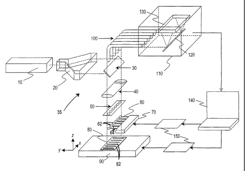
Fig. I shows an apparatus, indicated generally at 35, for examining the
identity of chemical groups in a sample attached to a surface. Shown in the
figure is a scanning stage 90, and carried on the stage, a DNA chip 80 having
a
plurality of stretched DNA strands, such as strands 82 anchored on the chip
surface and disposed parallel to one another. Methods for anchoring stretch
7
CA 02521016 2005-09-29
WO 2004/090505 PCT/US2004/010544
polymer strands, such as DNA strands on a chip surface will be described
below.
According to an important feature in this embodiment, the surface of the chip
on
which the sample is supported has a mirror coating of a plasmon resonance
metal, e.g., silver, gold, or aluminum.
The DNA strands are scanned by scanning stage 90 such as a
piezoelectric, or electromagnetic motion control stage. A stage with
electromagnetic motion control allows a scan area up to tens of centimeters
and
more, thus allowing scanning single molecule DNA chips with total individual
chromosomes.
A light beam with preferably coherent, circularly polarization is generated
by a laser 10. The laser may include two lasers for performing nonlinear Raman
spectroscopy such as CARS and Femtosecond Induced Raman Spectroscopy
(D. McCamant). An exemplary laser system uses a Ti-Sapphire tunable laser
with pulsed and continuous mode of operation. The wavelength of excitation
light beam preferably is selected and tuned to be in close proximity to the
maximum spectral peak in the plasmon resonance absorption spectra of the
plasmon resonant substrate. In case scanning with of plasmon nanolens
plasmon resonance absorption spectra of whole system (plasmon nanolens +
plasmon resonant substrate) should be considered in adjustment of frequency.
It
is important to note that because of nanoscopic proximity of plasmon nanolens
to surface of plasmon resonant substrate spectra of plasmon absorption are
changed.
The light beam is expanded by means of beam expander, or is
transformed into scanning beam in a beam raster 20. In this way, a single
light
beam is split into an array of light beams each directed into individual
plasmon
nanolens in array of nanolens 60. Each individual light beam is directed
through
a beam splitter 30 and collimation optics 40 onto a microlens array 50. The
microlens array allows individual digital control of each individual light
beam
directed into individual plasmon nanolenses, such as lenses 62 in array 60,
carried at the free end of cantilever beams, such as beam 64, as will be
described in greater detail below.
8
CA 02521016 2011-05-31
As will be appreciated below, the plasmon gap mode nanolens disclosed
in the present invention is based on the ability of localized plasmons
(collective
oscillations of electrons) excited inside metal nanoparticles by external
electromagnetic wave to enhance electromagnetic fields in a near-field zone in
close proximity to a plasmon resonance surface and to localize it in extremely
small nanoscale volumes. This non-propagating electromagnetic field is
concentrated in close proximity (few tens of nanometers 30-40 nm) near
nanoparticle surfaces and is named as "near field electromagnetic field" to
distinguish it from propagating electromagnetic field in far field zones.
With continued reference to Fig. 1, the light beam applied to each
plasmon nanolens in the cantilever-beam array may be modulated by a
micromachined mirror assembly 50 such as sold by Texas Instruments, Inc.,
Dallas, Texas, under the tradename "Digital Micromirror Device". This system
allows digital control of each individual plasmon nanolens illumination and
read
out signal scattered from each plasmon nanolens. This system is especially
useful for implementing of digital control of high speed programmed
individually
addressable multichannel pulsed mode illumination and acquisition of scattered
signal that is crucial for implementing ultra rapid direct DNA sequencing with
direct digitizing of sequence information into computer memory.
The distance between the plasmon nanolens and sample DNA is
maintained by a feedback cantilever bending system. Such control systems are
well known and described for atomic force microscopes, e.g., in U.S. Patent
No.
5,883,705, or near field scanning optical microscopes, e.g., in U.S. Patent
No.
5,354,985. One method for
of individual actuation and control of each cantilever beam in array 60 during
a
scanning process employs piezo-resistor feedback control, as disclosed detail
in
the US Patent No. 6,441,359.
The distance between each plasmon nanolens and the associated DNA
sample is preferably maintained at the level of 0.1 nm to few nanometers in
order to achieve optimum field amplification and localization in gap between
nanolens and DNA sample and surface of substrate by excitation of near field
electromagnetic gap modes as it shown on Fig. 2 and 6a and 6b. As the gap
9
CA 02521016 2005-09-29
WO 2004/090505 PCT/US2004/010544
between each nanolens and the substrate surface on which the sample is
carried varies, the localization and intensity of electromagnetic gap modes
varies
also. Therefore, by changing the distance between nanolens and DNA sample
(or substrate surface) it is possible to control the shape and localization of
electromagnetic gap modes, for the purpose of achieving maximum scattered
light (read out) signal and maximum spatial resolution. By optimizing these
gap
modes, it is possible to achieve a level of resolution that allows
discrimination
between individual bases in a DNA strand immobilized on the surface of the
substrate. Depending on the level of overstretching of the DNA strands on a
chip, the requirements for spatial resolution may vary from base to base, and
from strand to strand. However, the distance is in a range of a few nanometers
to less than 1 nanometer.
In the embodiment shown in Fig. 1, light reflected in backscattering
geometry from each plasmon nanolens interacting with individual DNA bases is
directed back through microlens array 50, collimation optics 40, and a beam
splitter 30 into receiving end of optical fiber ribbon 100. It will be
understood,
however, that the invention is not limited to backscattering collection of
light. In
other implementations of invention illumination and collection geometry may be
other from backscattering geometry, in which case light illumination and
collection optical systems may be separated.
Scattered signal light through optical fiber ribbon 100 is directed onto the
slit of a monochromator of a multichannel spectral analyzer 110. Notch filters
are
employed to eliminate incident light. A diffraction grating 120 splits
scattered
light beam into set of monochromatic light beams that will be transformed into
individual Raman spectra. Spectra obtained on detector array 130 are then
converted into digital form and transmitted into computer 140 where they are
processed to produce sequence information of DNA samples on the chip.
Another suitable optical design, not shown here, utilizes interferometric
detection
method, such as has been previously disclosed (e.g., F. Zenhausen).
CA 02521016 2005-09-29
WO 2004/090505 PCT/US2004/010544
C. Nanolens operation and fabrication
This section describes specific nanolens structures designed to be placed
in close proximity to the smooth metallic surface of the sample substrate, to
produce localized gap modes when the lens is illuminated by a a light beam,
e.g., a coherent and/or circularly polarized light beam. These modes can be
used for direct optical reading of molecules, placed in a space between the
nanolens of mirror substrate surface, with high spatial resolution for
achieving
sub-nanometer resolution, and with signal amplification allowing detection of
spectral signature of single small molecule such as individual bases of DNA
strands.
The most general design of a nanolens includes one and preferably a
plurality (e.g., 2-6) metal nanoparticles having selected shapes and selected
particle geometries with respect to each other. A preferred particles geometry
is
a symmetrical arrangement of the particles about a central axis, as will be
illustrated below, although other geometries, such as disordered fractal, are
also
contemplated. The nanoparticles forming the lens may have different shapes
and dimensions and are placed in nanoscopic proximity to each other. However
the largest dimension of each nanoparticle and of the system as a whole do not
exceed the wavelength of the illuminating light. Nanoparticles in the size
range
between 5-200 nm, e.g., 20-50 nm are preferred.
Fig. 2 is a detailed perspective view of a portion of a cantilever beam 160
carrying a six-particle nanolens 180 at its free (distal) end. As seen, a
circularly
polarized light beam 190 from laser source is directed through confocal lens
optics 50 onto a nanolens 180. The nanolens is mounted on a holder 170
formed of transparent dielectric material, which could be in one embodiment
the
free end of cantilever 160 used to controls the distance between a nanolens
and
the sample in scanning probe device. The nanolens is placed in close proximity
to a metal mirror surface 200 on the sample substrate. Since far field light
directed by the confocal optics can be focused to a spot size around or
slightly
less than 1 micron, which is determined by diffraction optics limit, and
diameter
of the nanolens (the diameter of the circle circumscribing the nanolens
particles
182) is preferably in the range of 50 -200 nm, that is, less than the
wavelength
11
CA 02521016 2005-09-29
WO 2004/090505 PCT/US2004/010544
of the illumination light. Also as seen in the figure, the light illumination
area
(dotted-line circle indicated at 350) is usually larger than area of nanolens.
However, it is possible to create a nanolens of 0.5 -1.0-micron diameter so
that
it will match focal spot. In that case, the nanolens will work as a
nanoantenna,
which will concentrate electromagnetic energy to the center of nanolens
through
excitation of localized plasmons.
In the embodiment shown in Fig. 2a, plasmon nanolens 185 has a star
like structure consisting of six metal nanoparticles, such as particles 182,
each
particle having a shape of either a prolate spheroid with a large eccentricity
(preferably more than 5), or a cylindrical nanorod with hemisphere caps at the
ends, or a metal nano wire. This particle geometry is also seen at 185 in Fig.
2B, along with nanolens particle configurations 195, 205, 215, and 225 for
lens
with five, four, three, and two particles, respectively.
As noted above, illumination of each nanolens is preferably by a laser
beam or non-coherent electromagnetic wave with circular polarization. Maximum
enhancement of the electromagnetic field, indicated at 200 in Fig. 2a, is
achieved in the central part of the lens close to axis of nanolens. This
region has
diameter of a few nm or less. Field amplification factor up to 1500-3000 may
be
achieved in the center of nanolens as it is illustrated by results of
numerical
simulation described below with respect to Figs. 6a-6c, 7a-7c, and 8 8, below.
That amplification factor significantly exceeds the amplification achievable
in
configurations consisting of spherical nanoparticles and other shapes of
nanoparticles known from prior art. Maximum local field amplification achieved
in
numerical simulation of 300 was reported (H. Xu).
The nanolens of the invention may be constructed by a variety of known
methods. In general, the nanolens is fabricated integrally with the cantilever
beam using established nanofabrication methods based on electron beam
lithography or focused ion beam lithography (G.R. Brewer), or based on
Scanning Tunneling Microscopy Lithography. Another method of fabrication may
be based on template assisted self-assembling (Y. Xia). Alternative methods
such as dip-pen nanolithography can be used to create plasmon nanolens
patterns on different support materials (e.g., D. Ginger) or DNA based self-
12
CA 02521016 2011-05-31
assembling technique (e.g., C. M. Niemeyer). In one embodiment plasmon
nanolens may be integrated into at free end of cantilever that is part of
scanning
probe device, and can simultaneously perform function of cantilever tip that
control distance between nanolens and sample during scanning in scanning
probe devices such as Atomic Force Microscope - AFM or Scanning Near Field
Optical Microscope - SNOM. One possible implementation of plasmon nanolens
integrated into cantilever of scanning probe spectroscopic device is presented
in
Fig. 3.
Fig. 3 illustrates how plasmon nanolens may be integrated into a free end
of cantilever of scanning probe spectroscopic device, and can simultaneously
perform the function of a cantilever tip that control distance between the
nanolens and sample during scanning of the sample. Cantilever 160 is prepared
from a composite material that has an opaque material portion 260 and an
optically transparent portion 170 that forms optical window 250, allowing
incident
circularly polarized light to interact with nanolens 180 and to excite
effectively
localized plasmas (LP) and gap modes (GM).
D. Preparation of sample-containing substrate
The substrate or support in the apparatus is designed to enhance
electromagnetic field in close proximity to surface, and is coated with a thin
film
of a plasmon resonant material, such as a silver, gold, or aluminum. Film
thickness is preferably between 25-200 nm, e.g., 50 nm. Suitable substrate,
e.g., glass substrates can be coated with the metal film by known methods,
such
as vacuum evaporation or rf sputtering techniques. Exemplary substrate
coatings and methods of their production are disclosed in US patent 5,611,998
for "Optochemical sensor and method for production," and in the reference to
V. Matyushin.
DNA strands with lengths, for example, from 100 nanometers up to 2.5
millimeters are placed on a substrate as shown at 82 in Fig. 1. The distance
between strands should be in the range of 200 -300 microns and should
correspond to the distance between adjacent cantilevers in cantilevers array.
13
CA 02521016 2011-05-31
Preferable is distance 250 micron, which correspond to pitch of 250 micron,
which is standard pitch in optical fiber ribbon applications.
Fig. 4 shows an exemplary chip or substrate 80 for use in the apparatus
and method of the invention. As shown here, samples of DNA obtained, for
example, from genomic DNA, in the form of single-stranded DNA fragments with
lengths up to 2.5 millimeters (5 Mbase). The strands, such as indicated at 210
are placed onto surface of slide with plasmon resonant optical enhancement
properties 80. They are placed in an ordered, addressable way. Each end of
DNA strand is attached to complimentary oligonucleotide on right/left barcode
220a and 220b. The distance between strands should be in the range of 200 -
300 microns and should correspond to the distance between adjacent
cantilevers in cantilevers array. Preferable is distance 250 micron, which
correspond to a pitch of 250 micron, which is in correspondence with pitch in
standard optical-fiber ribbon.
Methods for stretching and orienting linear polymer samples, such as
DNA, RNA, nucleic analogs, polypeptides, linear carbohydrates and the like,
are
known. For example, the opposite ends of the sample polymer, e.g., DNA, can
be covalently attached to microspheres, such as latex or glass beads, and the
beads are then manipulated by pulsed-laser molecular tweezers until a suitable
degree of stretching, and preferably overstretching, is achieved. This
approach
is illustrated in Fig. 4 which shows microspheres 290a, 290b attached to
opposite ends of DNA strand 210. Each sphere is "captured" by a laser beam,
such as beams 300a, 300b, for manipulating the spheres to stretch and orient
the strand for placement on the substrate surface. Once this placement is
achieved, end regions of the strand are anchored to the substrate by
hybridization with complementary oligonucleotides attached to the bar-code
region of the substrate. Methods for captuing and manipulating microspheres in
a laser beam are described, for example, in U.S. Patent No. 5,620857 and in
U.S. patent application 20040001371.
In a related approach, the ends of the polymer strand are covalently
attached to magnetic beads, or to a solid support and a magnetic bead, and
14
CA 02521016 2011-05-31
magnetic field(s) are applied to the bead(s) until an appropriate degree of
stretching and strand orientation are achieved. More generally, the opposite
ends of a strand may be attached to a pair of relatively moving supports, and
the
supports positioned until a desired degree of stretching and orientation are
produced, as disclosed, for example, in U.S. Patent No. 6,342,353.
Methods for drawing a charged polymer strand into a linear conformation
by electrophoresis in a narrow microchannel are also known.
Once the polymer strands are stretch and oriented for attachment to the
substrate, the sample molecule is anchored on the substrate by any of a number
of suitable anchoring methods. As noted above, the substrate may be provided
by end-regions oligonucleotides capable of hybridizing to the sequences at end
regions of a sample DNA strand. Where the strand is stretched by manipulating
particles covalently attached to the strand ends, the substrate may contain
chemical groups or magnetic structure for anchoring the particles to the
substrate, with the strand in a stretched condition. One common chemical
attachment chemistry for a gold surface is a thiol reagent covalently carried
at
end regions of the sample strand.
More generally, procedures for preparation of a substrate surface on
which DNA molecules are to be anchored are known to those of skill in the art
of
DNA hybridization detection methods (See for instance, J.P. Rabe).
E. Scanning and detection method
As indicated above, an important application of the apparatus and method
of the invention is in sequencing nucleic-acid samples such as chromosomal or
full genomic DNA. This section will describe the operation of the above
apparatus and the method of the invention with reference to this particular
application, it being understood that the same operation and method will apply
to
the examination of the chemical groups in any sample.
At its simplest, the method is used to examine one or more chemical
groups of a single molecule or collection of similar molecules localized at a
defined detection region on a substrate. In this application, a single
nanolens
CA 02521016 2005-09-29
WO 2004/090505 PCT/US2004/010544
carried, for example, at the free end of a cantilever beam is moved toward the
sample, e.g., in the distance range less than 10-40 microns, until a maximum
enhancement of a distinguishing enhanced Raman spectral feature is observed.
Alternatively, the spectral features may be recorded as the nanolens is moved
alternately toward and away from the sample surface, to yield a time-variant
spectrum of the sample. Nanolens oscillation in the range of between 0.1 to 10
nm, for example, could be used in generating the time-variant spectrum.
More generally, the method of the invention for examining the identity of
chemical groups in a sample, includes the steps of first attaching the sample
to a
substrate having a mirror surface on which the sample is supported, and which
is
formed of a plasmon resonant metal. A beam of light is directed onto a
nanolens
of the type described above to produce near-field electromagnetic gap modes in
a space between the nanolens and a confronting detection region on the
substrate surface, when the gap between the nanolens and substrate is 30 nm
or less. The lens assembly is then moved toward or away from the substrate
surface, with a spacing between the nanolens and substrate surface of less
than
40 nm, to produce electromagnetic gap modes that enhance the Raman
spectroscopy signals produced by the sample in the detection region. Light
emitted by or scattered from the sample at the detection region is received by
a
detected and converted into a gap-mode enhanced Raman spectrum, whereby
the sample chemical group at the detection region can be identified.
Where the sample contains a plurality of groups arranged along a linear
portion of the sample molecules, as in the case of a nucleic sample for
identification of successive base groups, the procedure just described is
applied
to each base successively, as the nanolens is moved relative to the substrate.
This movement may be carried out by cantilever translation relative to a
stationary substrate of substrate stage movement relative to a stationary
nanolens. As the nanolens is placed at each successive position, it is then
moved toward or away from the sample to find the optimal detection distance,
or
to generate a time-variant spectrum, as described above. The lens and sample
bases may be kept in registry by one of a variety of registration techniques.
For
example, a "control" nanolens could track the detect bases in a known-sequence
16
CA 02521016 2005-09-29
WO 2004/090505 PCT/US2004/010544
DNA sample carried on the substrate. By tracking this sequence, along with one
or more unknown-sequence samples, the apparatus can confirm that the relative
movement between lenses and substrate is acting to preserve registration
between sample and successive DNA bases. Alternatively, one of the cantilever
beams in the apparatus may be a scanning atomic-force microscope tip for
detecting movement of the tip over each base of a control DNA strand, as the
array of cantilever devices are moved along the DNA strands.
In a more usual application, a plurality of linear sample strands, e.g., DNA
strands are aligned on a single substrate, for simultaneous reading by a
plurality
of nanolenses, as illustrated at 82 in the apparatus of Fig. 1. Figs. 5a and
5b
illustrate this operation as applied to reading a plurality of stretched,
aligned DNA
strands, such as strand 210, carried on a substrate 310. Although the figures
show a single lens assembly composed of a cantilever beam 160 carrying a
nanolens 180 at its free end, it will be understood that the apparatus
includes an
array of lens assembly, one for each of the aligned strands on the substrate.
As the group of lens assemblies are moved along the substrate, each lens
assembly is adjusted vertically (in a direction toward the substrate) to
optimize
spectral signal. As seen in Fig. 5b, this vertical movement is effective to
place
the gap modes produced by the concentration of near-field electromagnetic
modes between the lens, formed by PRPs such as at 185, with the plasmon
resonant surface, indicated at 310.
The enhanced Raman spectra of each strand chemical group (base) are
consecutively measured using a multichannel Raman spectrograph and are
digitized by means of two-dimensional ICCD array with digital recording. The
signal from the Raman spectrometer is stored in computer memory for further
analysis. The final results are obtained in a form of sequence of bases of
nucleotides A,T,G,C. In a course of scanning procedure nanolens- tip will
detect
each base (A,T,G,C) in DNA strands both spectroscopic and topographically.
SERS spectra are registered consecutively for each base which will allow
identifying each particular base (A,T,G,C) in DNA strand by its unique enhance
spectral signature that is characteristic of that base, allowing direct de
novo
sequencing of individual fragments of DNA molecule. SERS spectra of A, T, G,
17
CA 02521016 2005-09-29
WO 2004/090505 PCT/US2004/010544
and C obtained on plasmon resonant substrate are known to give distinctive
spectra that allow for the different bases to be identified. The present
invention,
by focusing the excitation field in a small gap between a lens and substrate,
and
exploiting gap-mode enhancement of the Raman signals, allows individual bases
of DNA to be identified, thus permitting direct base-by-base DNA reading.
The numbers of cantilevers with fiber optic tips which can be used in
array, are in principle unlimited; however, for one scan sequencing of the
largest
human chromosome (human chromosome No 1 containing about 263 million
bases), the apparatus would require about 100 lens assemblies, each reading a
fragment of about 2.5 - 3.0 Mbase. Assuming 0.01 sec sampling time, the
apparatus would complete sequence of this chromosome in less than about 10
hour of scan time. Using this device practically it is possible to implement
in
parallel up to few hundred channels in array (1 DNA strands per channel) with
sampling speed of 0.01 to 1 second per base.
More generally, the method of the invention for examining the identity of
chemical groups in a sample, includes the steps of first attaching the sample
to a
substrate having a mirror surface on which the sample is supported, and which
is
formed of a plasmon resonant metal. A beam of light is directed onto a
nanolens
of the type described above to produce near-field electromagnetic gap modes in
a space between the nanolens and a confronting detection region on the
substrate surface, when the gap between the nanolens and substrate is 4 nm or
less. The lerns assembly is then moved toward or away from the substrate
surface, with a spacing between the nanolens and substrate surface of less
than
40 nm, to produce electromagnetic gap modes that enhance the Raman
spectroscopy signals produced by the sample in the detection region. Light
emitted by or scattered from the sample at the detection region is received by
a
detected and converted into a gap-mode enhanced Raman spectrum, whereby
the sample chemical group at the detection region can be identified.
The degree of Raman spectra amplification achievable with the present
invention can be appreciated from Figs. 6-8. In these figures, electromagnetic
field strength E was calculated by modeling the system and solving Maxwell's
equations in a near-field approximation using an integral equation
approximation.
18
CA 02521016 2005-09-29
WO 2004/090505 PCT/US2004/010544
Fig. 6a shows the variation in E as a function of eV for a three-particle
lens. The
field distribution in the central region of the lens is shown in Fig. 6C. Fig.
6b is a
plot of field strength taken along the y axis in Fig. 6C, along the line x=0.
As
seen, field strength amplification reaches a maximum of about 1,400
(amplification over incident light) at the point y=0.5, close to the upper
particle in
Fig. 6c.
A similar set of plots is shown in Figs 7a-7c, but where the lens here is
constructed of four symmetrical particles, as seen from the field distribution
diagram in Fig. 7c. Fig. 7b shows a symmetrical distribution of E along the
line x
equal zero as the y coordinate varies from the bottom to the top. When the
plot
is constructed along the diagonal line between -1, -1 and +1, +1, the plot
seen in
Fig. 8 is achieved, showing an amplification of nearly 3000 at points near
between the particles away from the center.
According to prevailing mechanism, Raman enhancement is
electromagnetic mechanism, where Raman signal is proportional to E4 (
M.Moskovits, Rev. Mod. Phys. v. 57, p. 783, 1985 ) where E is local
enhancement of field in the area of molecule. In the case of a field
amplification
factor 500, the Raman signal enhancement would be 5004 =6.25 1010, which is
significantly higher than has been reported in the literature. To obtain this
enhancement, the sample molecule should be in center of a multi-particle
nanolens. However, if the molecule is also close to a plasmon resonance
surface, the field enhancement can be as high as 3,000, giving a Raman signal
enhancement of up to 8.1 x 10¹⁵, allowing single molecule chemical groups to
be
detected.
Although the invention has been described with respect to particular
embodiments and applications, it will be understood that various changes and
modification may be made without departing from the invention.
19