Note: Descriptions are shown in the official language in which they were submitted.
CA 02521498 2009-07-28
WO 2004/088755 PCTIGB2004/001406
NANOWHISKERS WITH PN JUNCTIONS AND METHODS OF FABRICATING THEREOF
Background of the Invention
Field of the Invention
This invention relates generally to structures and devices produced by
techniques of nanotechnology.
More specifically, the invention relates to such structures and devices
incorporating at least one element, essentially in one-dimensional form, and
that is of
nanometer dimensions in its width or diameter, and that preferably is produced
by the
so-called Vapor-Liquid-Solid (VLS) mechanism. For the purposes of this
specification, such element will be termed a "nanowhisker".
Brief Description of the Prior Art
Nanotechnology covers various fields, including that of nanoengineering,
which may be regarded as the practice of engineering on the nanoscale. This
may
result in structures ranging in size from small devices of atomic dimensions,
to much
larger scale structures for example on the microscopic scale. Commonly, such
structures include nano structures. In certain contexts nanostructures are
considered to
be those having at least two dimensions not greater than about 100 nm, with
some
authors using the term to identify structures having at least two dimensions
not
greater than about 200 nm. Nevertheless, some procedures for fabricating such
small
structures are useful for structures having at least two dimensions somewhat
greater,
e.g., structures having at least two dimensions not greater than about
1 micrometer ( m). Ordinarily, layered structures or stock materials having
one or,
more layers with a thickness less than 1 m are not considered to be
nanostructures.
Thus, although the term "nanostructure" is more classically considered to
refer to
structures having at least two dimensions not greater than about 100 nm, in
the
following discussion, the term "nanostructure", "nanowhisker", or
"nanoelement" is
CA 02521498 2005-10-04
WO 2004/088755 PCT/GB2004/001406
intended to include a structure having at least two dimensions not greater
than about
1 m.
Nanostructures include so-called one-dimensional nanoelements, essentially
in one-dimensional form, that are of nanometer dimensions in their width or
diameter,
and that are commonly known as nanowhiskers, nanorods, nanowires, nanotubes,
etc.
As regards nanowhiskers, the basic process of whisker formation on
substrates, by the so-called VLS (vapor-liquid-solid) mechanism, is well
known. A
particle of a catalytic material, usually gold, for example, on a substrate is
heated in
the presence of certain gases to form a melt. A pillar forms under the melt,
and the
melt rises up on top of the pillar. The result is a whisker of a desired
material with
the solidified particle melt positioned on top. (See E.I Givargizov, Current
Topics in
Materials Science, Vol. 1, pages 79-145, North Holland Publishing Company,
1978.)
The dimensions of such whiskers were in the micrometer range.
Although the growth of nanowhiskers catalyzed by the presence of a catalytic
particle at the tip of the growing whisker has conventionally been referred to
as the
VLS (Vapor-Liquid-Solid) process, it has come to be recognized that the
catalytic
particle may not have to be in the liquid state to function as an effective
catalyst for
whisker growth. At least some evidence suggests that material for forming the
whisker can reach the particle-whisker interface and contribute to the growing
whisker even if the catalytic particle is at a temperature below its melting
point and
presumably in the solid state. Under such conditions, the growth material,
e.g., atoms
that are added to the tip of the whisker as it grows, may be able to diffuse
through a
the body of a solid catalytic particle or may even diffuse along the surface
of the solid
catalytic particle to the growing tip of the whisker at the growing
temperature.
Evidently, the overall effect is the same, i.e., elongation of the whisker
catalyzed by
the catalytic particle, whatever the exact mechanism may be under particular
circumstances of temperature, catalytic particle composition, intended
composition of
the whisker, or other conditions relevant to whisker growth. For purposes of
this
application, the term "VLS process", "VLS method", or "VLS mechanism", or
equivalent terminology, is intended to include all such catalyzed procedures
wherein
nanowhisker growth is catalyzed by a particle, liquid or solid, in contact
with the
growing tip of the nanowhisker.
International Application Publication No. WO 01/84238 discloses in Figures
15 and 16 a method of forming nanowhiskers wherein nanometer sized particles
from
-2-
SUBSTITUTE SHEET (RULE 26)
CA 02521498 2005-10-04
WO 2004/088755 PCT/GB2004/001406
an aerosol are deposited on a substrate and these particles are used as seeds
to create
filaments or nanowhiskers.
For the purposes of this specification the term nanowhiskers is intended to
mean "one-dimensional" nanoelements with a width or diameter (or, generally, a
cross-dimension) of nanometer size, the elements having been formed by the so-
called VLS mechanism. Nanowhiskers are also referred to in the art as
"nanowires"
or, in context, simply as "wires", and such terminology, as used in this
application, is
equivalent to the term "nanowhiskers".
Several experimental studies on the growth of nanowhiskers have been made,
including those reported by Hiruma et al. They grew I11-V nano-whiskers on III-
V
substrates in a metal organic chemical vapor deposition (MOCVD) growth system.
(See K. Hiruma, et al., J. Appl. Phys. 74, page 3162 (1993); K. Hiruma, et
al., J.
Appl. Phys. 77, page 447 (1995); K. Hiruma, et al., ICE Trans. Electron. E77C,
page 1420 (1994); K. Hiruma, et al., J. Crystal Growth 163, pages 226 - 231
(1996)).
Hiruma et al. have made pn junctions within nanowbiskers by doping GaAs
whiskers with Si using Si2H6, during the growth process, and switching the
dopant to
an -opposite conductivity type (carbon) during growth: K. Hiruma et al., J.
Appl. Phys.
77(2), 15 January 1995 p.447, see pages 459-461; and K. Hiruma et al J. Appi.
Phys.
75(8) 4220 (1994). In general, there are problems in that the definition of
the
junction within the nanowire is not good enough for electrical components, and
in
that the presence of dopant ions within the crystal creates crystal
imperfections and
reduces carrier mobility.
In another approach by Lieber et al, WO-A-03/005450, nanowires were
produced, different wires being doped with opposite conductivity type dopants,
and
two wires of opposite conductivity type were physically crossed, one on top of
the
other, so that a pn junction was formed at their point of contact. A
difficulty with this
approach is the extra step required of physically positioning the nanowires.
In planar semiconductor processing, various doping techniques are known.
One technique that is valuable with heterojunctions is known as modulation
doping.
In this technique, carriers from a doped layer of, e.g., AlGaAs, diffuse
across an
interface with an undoped material, e.g., GaAs, and form a very thin layer of
carriers
of very high mobility, within a potential well, next to the interface - see
for example
Fig. 1 of WO 02/19436.
-3-
SUBSTITUTE SHEET (RULE 26)
CA 02521498 2009-07-28
WO 2004/088755 PCT/GB2004/001406
U.S. Patent 5,362,972 discloses an FET wherein the current flowpath between
source and drain is composed of GaAs nanowhiskers. The nanowhiskers are
surrounded by n-doped AlGaAs, to create by modulation doping a one-dimensional
electronic gas within each nanowhisker.
WO 02/020820 discloses a modulation doping technique in Coaxial
Heterostructure Nanowires, wherein dopants in an outer coaxial layer donate
free
carriers to an inner nanowire.
In other techniques, doping of a semiconductor region in a planar
semiconductor device occurs by diffusion of ions from an adjacent region of
polymer;
see Guk et al., Semiconductors Vol. 33(3), pp. 265-275, March 1999.
In U.S. Patent No.7335,908, the application for which was filed July 7. 2003
in the
names of Samuelson and Ohisson, a process was disclosed for producing
nanowhiskers. and
structures were disclosed incorporating nanowhiskers.
Summary of the Invention
It is an object of the invention to provide new and improved nano-engineered
structures incorporating nanowhiskers and other one-dimensional nanoelements,
the
nanoelements having improved conductivity characteristics.
It is a further object of the invention to provide new and improved nano-
engineered structures incorporating nanowhiskers and other one-dimensional
nanoelements, wherein the nanoelements contain improved pn junctions.
In at least a preferred embodiment of the invention, nanowhiskers or other
one-dimensional nanoelements are grown as pure crystals without doping. The
nanowhisker is then enclosed in an enclosure comprising a surrounding layer or
matrix of a further different material that will usually be a semiconductor
material.
Dopant ions are incorporated into this further material, by an appropriate
process
during or after its deposition. Carriers liberated in the further material
transfer into
the nanowhisker. The band structures of the nanoelement and the further
material
ensure that it is energetically favorable for the carriers to diffuse into the
nanoelement; this is effectively by the process known as modulation doping
wherein
a potential well is defined within the nanowhisker. Thus effectively the
nanowhisker
is doped with carriers, but that these are of high mobility, since the absence
of dopant
ions within the nanowhisker ensures that the crystalline structure is not
deformed.
-4-
CA 02521498 2005-10-04
WO 2004/088755 PCT/GB2004/001406
The preferred embodiment provides a method of producing a one-dimensional
nanoelement of desired conductivity, the method comprising the steps of (1)
forming
a one-dimensional nanoelement of a first material, (2) surrounding the
nanoelement
with a second material, different from that of the nanoelement, the second
material
containing dopant material whereby charge carriers from the dopant material
diffuse
into the nanowhisker to create said desired conductivity. More specifically,
the
method comprises the steps of (1) forming by the VLS method a nanowhisker on a
substrate, the nanowhisker including a first semiconducting material, and (2)
forming
a coaxial layer around the nanowhisker of a second semiconducting material,
and (3)
incorporating dopant material into the coaxial layer whereby charge carriers
from the
dopant material diffuse into the nanowhisker to create said desired
conductivity.
The invention provides a means of creating a pn junction within a one-
dimensional nanoelement by modulation doping.
Specifically the invention provides a nanoengineered structure including a
one-dimensional nanoelement of a first semiconducting material having a first
bandgap, an enclosure comprising at least one second material having a second
bandgap enclosing said nanoelement along at least part of its length, and said
second
material being doped to provide opposite conductivity type charge carriers in
respective first and second regions along the length of the of the
nanowhisker,
whereby to create by transfer of charge carriers into said nanoelement,
corresponding
first and second regions of opposite conductivity type charge carriers with a
pn
junction therebetween in said nanoelement, and wherein the bandgaps are such
that it
is energetically favorable for the charge carriers to remain in said
nanoelement.
The enclosure for the nanoelement may be a coaxial jacket. In one preferred
form a thin nanowhisker of GaAs is grown, then the growth conditions are
changed
from those appropriate for catalytic growth to those appropriate for bulk
growth, so
that a coaxial jacket is formed around the sides of the nanowhisker. The
material
maybe AlGaAs. It is necessary to dope the lower part of the AlGaAs jacket with
one
conductivity type dopant material, and the upper parts of the coaxial jacket
with
opposite conductivity dopant ions. One exemplary technique for achieving this
is to
embed the coaxial jacket within a polymer matrix comprising upper and lower
layers
as, for example, spin on glass or polymer substances. The lower layer has one
conductivity type dopant material, and the upper layer has the opposite
conductivity
type dopant material. Rapid thermal annealing causes diffusion of the dopant
-5-
SUBSTITUTE SHEET (RULE 26)
CA 02521498 2005-10-04
WO 2004/088755 PCT/GB2004/001406
material into the coaxial jacket. The thermal annealing step is stopped before
appreciable diffusion into the one-dimensional nanoelement. The presence of
the
dopant ions within the coaxial jacket creates modulation doping within the
nanowhisker, and a pn junction between the two regions of opposite
conductivity type
material. The space charge within each region is maintained within the
nanoelement,
and the depletion region of the pn junction maybe sharp or as diffuse as
desired
(typically within the range 50 urn to 1 gm). The diameter of the nanowhisker
is
preferably small, about 20 rim. The coaxial jacket may be as small as 10 rim
thick,
but it may in other cases be preferable to have a jacket that is 200 nm thick
or one that
even fills the volume between the nanowires completely in an array of
nanowires.
The materials of the nanowire and jacket may be GaAs and AIGaAs, for
example. Other material combinations could be InAs in the core section and
AlSb in
the surrounding material or a germanium core and a silicon jacket.
In a modification, the coaxial jacket is doped in one conductivity type during
its formation. A layer of spin-on glass is then formed partway along the
length of the
nanowire, containing opposite type conductivity ions, that are sufficiently
concentrated to reverse the conductivity type in the lower part of the coaxial
jacket.
In a further modification, the coaxial jacket is grown in an undoped
condition, and a
layer of spin-on glass is then formed partway along the length of the
nanowire,
containing one type conductivity ions. The structure is then exposed to a gas
containing opposite type conductivity ions that diffuse into the upper part of
the
coaxial jacket, where they create a region of opposite conductivity type. The
ions in
the gas also diffuse into the layer of spin on glass, but not in a sufficient
concentration
to overcome the existing concentration of the one type conductivity. A pn
junction is
thereby formed in the nanowire.
In an alternative form, the one-dimensional nanoelement is encapsulated
within an enclosure formed by first and second layers of polymer material or
spin on
glass, each layer having opposite conductivity dopant material. Direct charge
transfer
of the carriers from the polymer matrix creates modulation doping within the
nanowhisker, and two separate regions of oppositely signed charge carriers
with a pn
junction between them.
In a further alternative form of the invention the doping is so heavy as to
create degenerate doping within the nanoelement, that is to say the Fermi
level exists,
-6-
SUBSTITUTE SHEET (RULE 26)
CA 02521498 2005-10-04
WO 2004/088755 PCT/GB2004/001406
in one region, in the conduction band, and in the other region, in the valence
band. In
this state, the nanoelement comprises a tunnel diode or Esaki diode wherein in
known
manner, forward biasing of the junction creates a negative resistance caused
by
tunnelling between the valence and the conduction bands.
In a further aspect, a nanowhisker or other one-dimensional nanoelement is
surrounded by a material containing dopant ions. For example the surrounding
material may be a polymer material. By a process, for example a subsequent
step of
rapid thermal annealing, the dopant ions in the matrix material are permitted
themselves to diffuse into the nanowhisker, to create a desired conductivity.
This
provides advantages over a direct doping into the nanoelement, by providing an
extra
degree of control over the doping process, and permitting the diffusion of
certain
dopants into the nanoelement that would not be possible by a more direct
process.
Although a polymer material is preferred, which is evaporated or spun onto a
substrate so as to surround the nanowhisker, other materials may be employed,
such
as for example semiconductor material or dielectric material grown onto the
substrate.
The dopant material may be incorporated in the surrounding material before
application to the substrate, during the application to the substrate, or as a
subsequent
step after the surrounding material is formed on the substrate.
Specifically, the invention provides a method of forming a one-dimensional
nanoelement of a desired conductivity, comprising:
(a) forming a one-dimensional nanoelement on a substrate, the nanoelement
being
formed of a first material;
(b) forming at least a first layer of a further material on the substrate and
surrounding, at least partially, the nanoelement, the further material having
a first
conductivity type dopant material therein, and
(c) processing the further material so that said dopant material diffuses into
the
nanoelement, whereby to create a desired conductivity therein.
Additionally, the invention provides a nanoengineered structure, comprising a
one-dimensional nanoelement, of a first material, disposed on a substrate, and
at least
a first layer of material formed on the substrate and surrounding, at least
partially, the
nanoelement, the first layer having a first conductivity type dopant material
therein,
said first conductivity type dopant material having diffused into the
nanoelement,
whereby to create a desired conductivity within the nanoelement.
-7-
SUBSTITUTE SHEET (RULE 26)
CA 02521498 2005-10-04
WO 2004/088755 PCT/GB2004/001406
In a further aspect, a pn junction is created within a one-dimensional
nanoelement, preferably a nanowhisker. A nanowhisker is grown on a substrate,
and
embedded in a surrounding material. The material consists of first and second
layers,
formed on the substrate, one on top of the other, for example as polymer
layers
evaporated or spun onto the substrate. Alternatively the layers may be of some
other
material, for example dielectric material or semiconducting material grown on
the
substrate. The first layer extends partway up the nanowhisker, and has a first
dopant
material incorporated within it or subsequently injected, providing charge
carriers of
a first type. The second layer extends towards the top of the nanowhisker, and
has a
second dopant material contained within it or subsequently injected into it,
providing
charge carriers of an opposite conductivity type. The surrounding material is
treated,
as for example by rapid thermal annealing, so that the dopant ions themselves
diffuse
into the respective first and second regions of the nanoelement, to create an
effective
pn junction within the nanowhisker. In this case, the surrounding layers may
be
commercially available polymer layers evaporated or spun onto the substrate.
The
dopant materials are incorporated into the polymer materials before, during,
or after
the application of the polymer materials to the substrate.
In either case, the effective pn junction can be made as sharp as desired,
approaching that of a few nanometers. More than one pn junction may be created
by
employing multiple layers, each layer having appropriate dopant material.
Specifically the invention provides a nanoengineered structure including a
one-dimensional nanoelement with at least one pn junction therein, comprising
a
nanowhisker upstanding from a substrate, and a first layer of a material
formed on the
substrate and surrounding and extending partway up the nanowhisker, the first
layer
having a first conductivity type dopant material therein, and a second layer
of
material formed on top of the first layer and surrounding and extending
towards the
top of the nanowhisker, and having a second conductivity type dopant material
therein, whereby to create by diffusion from said first and second layers into
respective first and second regions of the nanowhisker, a pn junction within
the
nanowhisker between the first and second regions.
The invention also provides a method of forming a one-dimensional
nanoelement with a pn junction therein, comprising:
(a) forming a nanowhisker upstanding from a substrate,
-8-
SUBSTITUTE SHEET (RULE 26)
CA 02521498 2005-10-04
WO 2004/088755 PCT/GB2004/001406
(b) forming a first layer of material on the substrate and surrounding and
extending partway up the nanowhisker, the first layer having a first
conductivity type
dopant material therein, and
(c) forming a second layer of material on top of the first layer and
surrounding
and extending towards the top of the nanowhisker, and having a second
conductivity
type dopant material therein, so that diffusion from the first and second
layers into
respective first and second regions of the nanowhisker creates a pn junction
within
the nanowhisker between the first and second regions.
In a fifth aspect, the invention recognises that there are problems in
chemical
doping of dopant ions in a nanowhisker of III-V semiconductor material, since
for
most III-V semiconductors, solid solubility at room temperature is limited,
and during
cooling out-diffusion is fast with these nanodimensions. Thus the amount of
doping
within the nanowhisker may be difficult to accurately predetermine. The
invention
recognises that the interface between a nanoelement and a surrounding medium,
or a
heterojunction interface within a nanoelement, may have a stronger and more
significant role than hitherto realised in determining the electrical
characteristics of
the -nanoelement.
It is known that localised surface "trap" states exist at the surfaces of bulk
semiconductors; this is exhibited for example in Schottky diodes. This creates
what
is known as Fermi Level Pinning, where the surface trap states determine the
relative
levels of the conduction and valence bands in the junction materials. See,
e.g.,
"Defective Heterojunction Models", Freeouf J L, Woodall JM,: IBM Corp,:
Surface
Science, 1986, V 168 , N1-3 , P 518-530 .
The invention recognises that for a one-dimensional nanoelement, where there
may be a wide range of possibilities to combine III-V semiconductors in spite
of
lattice mismatch, Fermi Level Pinning is a constructive way to make pn
junctions by
choosing semiconductor alloy composition to determine carrier type. In such
devices
the band gap can be engineered and the carrier type can be controlled to make
new
types of semiconductor devices. When a semiconductor crystal ends abruptly at
an
interface, and "band bending" tends to occur to equalize the Fermi Levels on
the two
sides of the interface, Fermi Level Pinning, arising from the existence of
surface trap
states, counteracts this effect to reduce the amount of charge transfer across
the
interface.
-9-
SUBSTITUTE SHEET (RULE 26)
CA 02521498 2005-10-04
WO 2004/088755 PCT/GB2004/001406
The invention further provides a one-dimensional nanoelement including a
first segment of a first semiconductor crystalline material, and a second
segment of a
second semiconductor crystalline material different from that of the first,
and with a
heterojunction therebetween, whereby the first and second materials are
selected such
that charge carriers of opposite conductivity type are provided at the
opposite sides of
the heterojunction interface so as to create a pn junction with predetermined
characteristics, which characteristics are at least partially determined by
Fermi level
pinning.
The invention also provides a method of forming a pn junction comprising:
a. forming a one dimensional nanoelement having a first segment of a first
crystalline material, and a second segment of a second crystalline material
different
from that of the first, with a heterojunction therebetween,
b. the first and second materials being selected so as to provide charge
carriers of opposite conductivity type at the heterojunction so as to create a
pn
junction with predetermined characteristics, which characteristics are at
least partially
determined by Fermi level pinning.
In accordance with the invention, the charge carriers can be provided by the
intrinsic nature of the first and second materials. For III-V materials,
stoichiometric
compositions of ternary or quaternary materials can be chosen for desired
conductivity characteristics.
It has been found that the present invention is particularly applicable to III-
V
compounds epitaxially grown (CBE or MOCVD, or MOVPE), under group III rich
conditions. Under these conditions, the outermost atomic surface layers may
have
excess Ga or In ions and these create defect states, as further described
herein.
Brief Description of the Drawings
Preferred embodiments of the invention will now be described with reference
to the accompanying drawings, wherein:
Figure 1 is a schematic of the CBE apparatus used for making the described
embodiments.
Figure 2 is a cross-sectional schematic view showing a step in the formation
of the first embodiment of the invention, with an accompanying energy band
diagram.
-10-
SUBSTITUTE SHEET (RULE 26)
CA 02521498 2009-07-28
WO 2004/088755 PCT/GB2004/001406
Figure 3A shows a cross-section of a nanowhisker prepared by the VLS
method.
Figure 3B shows a cross-section of a nanowhisker having an enclosure or
jacket according to the invention.
Figure 3C shows an array of such clad nanowhiskers extending from a (111)
surface.
Figure 3D shows an enlarged view of a nanowhisker having been separated
from the surface.
Figure 3E is a view of the cross-section of the clad nanowhisker showing a
hexagonal structure that is characteristic of nanowhiskers growing in a <111>
direction.
Figure 3F is a luminescence curve showing characteristic peaks at
approximately 1.5 and 1.8 eV, which represent GaAs and AlGaAs materials
respectively.
Figure 4 is a cross-sectional view of a second embodiment of the invention.
Figure 5 is a cross-sectional schematic view of a third embodiment of the
invention.
Figure 6 is a cross-sectional schematic view of a fourth embodiment of the
invention.
Figure 7 is a cross-sectional schematic view of a fifth embodiment of the
invention.
Figure 8 is a cross-sectional schematic view of a sixth embodiment of the
invention.
Figure 9 is a graph showing the energy levels of the bands and surface states
of a number of semiconductor materials.
Figure 10 is a schematic energy level diagram for the doped nanowhiskers of
Figure 7 and Figure 8.
Description of the Preferred Embodiments
The. embodiments to be described are all formed with nanowhiskers,
preferably according to the Chemical Beam Epitaxy method (CBE) described in
copending U.S. Patent No.7,335,908
-11-
CA 02521498 2005-10-04
WO 2004/088755 PCT/GB2004/001406
As indicated above, in the following detailed description of the invention,
the
term "nanoengineered structures" signifies a structure that includes
structures, e.g.,
elements, parts, or the like, having dimensions as defined above, i.e.,
structures
having at least two dimensions less than about 1 micrometer. Such structures
are
referred to herein as "nanoelements" or nanostructures, and/or, because of
their
generally elongated shape, as "nanowhiskers" or "nanowires".
Chemical Beam Epitaxy (CBE) combines a beam epitaxial technique like
Molecular Beam Epitaxy (MBE) and the use of chemical sources similar to Metal
Organic Chemical Vapor Deposition (MOCVD). In MOCVD or related laser
ablation techniques, the pressure inside the reactor is usually greater than
10 mbar
and the gaseous reactants are viscous, which means that they have a relatively
high
resistance to flow. The chemicals reach the substrate surface by diffusion.
CBE
reduces the pressure to less than 10-4 mbar and the mean free path of the
diffusants
then becomes longer than the distance between the source inlet and the
substrate. The
transport becomes collision free and occurs in the form of a molecular beam.
The
exclusion of the gas diffusion in the CBE system means a fast response in the
flow at
the substrate surface and this makes it possible to grow atomically abrupt
interfaces.
The CBE apparatus shown in Figure 1 consists of a UHV growth chamber 100
where the sample 102 is mounted on a metal sample holder 104 connected to a
heater
106. Around the chamber there is a ring 108 filled with liquid nitrogen that
is called
the cryoshroud. The cryoshroud pumps away species that don't impinge or that
desorb from the substrate surface. It prevents contamination of the growing
surface
layer and reduces the memory effect. Vacuum pumps 110 are provided.
The sources 112 for CBE are in liquid phase and they are contained in bottles
which have an overpressure compared to the chamber. The sources are usually as
follows: TMGa, TEGa, TMIn, TBAs, and TBP. The bottles are stored in constant-
temperature baths and by controlling the temperature of the liquid source, the
partial
pressure of the vapor above the liquid is regulated. The vapor is then fed
into the
chamber through a pipe complex 114 to, in the end of the pipe just before the
growth
chamber, a source injector 116. The source injector is responsible for
injection of the
gas sources into the growth chamber 100, and for generation of a molecular
beam
with stable and uniform intensity. The III-material, from the metal organic
compounds TMIn (trimethylindium), TMGa (trimethylgallium) or TEGa
(triethylgallium), will be injected by low temperature injectors to avoid
condensation
-12-
SUBSTITUTE SHEET (RULE 26)
CA 02521498 2005-10-04
WO 2004/088755 PCT/GB2004/001406
of the growth species. They will decompose at the substrate surface. The V-
material
is provided by the metal-organic compounds, TBAs (tertiarybutylarsine) or TBP
(tertiarybutylphosphine). As opposed to the decomposition of the HI-material,
the V-
material will be decomposed before injection into the growth chamber 100, at
high
temperatures, in the injectors 116. Those injectors 116 are called cracking
cells and
the temperatures are kept around 900 C. The source beam impinges directly on
the
heated substrate surface. Either the molecule gets enough thermal energy from
the
surface substrate to dissociate in all its three alkyl radicals, leaving the
elemental
group III atom on the surface, or the molecule get desorbed in an
undissociated or
partially dissociated shape. Which of these processes dominates depends on the
temperature of the substrate and the arrival rate of the molecules to the
surface. At
higher temperatures, the growth rate will be limited by the supply and at
lower
temperatures it will be limited by the alkyl desorption that will block sites.
This Chemical Beam Epitaxy method permits formation of heterojunctions
within a nanowhisker, which are abrupt, in the sense there is a rapid
transition from
one material to another over a few atomic layers.
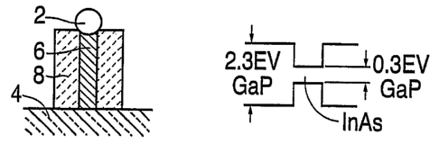
Referring now to Figure 2, a first embodiment of the invention is formed by
positioning a gold aerosol particle 2 on a III-V substrate 4, e.g., a gallium
arsenide
substrate. With appropriate conditions of temperature and pressure a
nanowhisker of
indium arsenide is grown by injecting organic materials TMIn and TBAs in a
conventional VLS procedure, e.g., in a chemical beam epitaxial method, using
the
apparatus described above, or by a metal organic vapor phase epitaxy (MOVPE),
or
the like. Indium and arsenide ions are absorbed in the gold particle 2 and
supersaturation conditions create a solid pillar 6 of indium arsenide.
. Once the indium arsenide whisker has been grown, different materials TEGa
and TBP are used to create a coaxial jacket or surrounding layer 8 of GaP
around the
nanowhisker 6. Layer 8 may be created by CBE; using the apparatus of Fig. 1,
wherein the conditions of temperature (106) and/or pressure (112) are changed
to
inhibit growth by the VLS mechanism, and instead to support bulk growth.
Alternatively the gold melt particle 2 can be removed mechanically, so that
subsequent growth of GaP will occur in bulk form
-13-
SUBSTITUTE SHEET (RULE 26)
CA 02521498 2005-10-04
WO 2004/088755 PCT/GB2004/001406
The resulting energy level bandgap diagram is shown with an energy gap of
2.3EV separating the conduction bands for gallium phosphide, whereas there is
a
bandgap of 0.3EV for the central indium arsenide whisker.
The jacket or shell material (GaP in this case) may then be doped, e.g., via
the
vapor phase, resulting in a sheath at the periphery of the GaP jacket which
will
contain donor dopants such as tellurium.
As an alternative to tellurium, any donor dopant materials that are commonly
used for GaP may be used, see for example CRC The Handbook of Chemistry and
Physics, Semiconductor Properties, e.g., Si, Sri, Te, Se, S, or the like.
Alternatively,
if an acceptor-doped jacket or shell is desired, appropriate acceptor
materials, e.g.,
Zn, Fe, Mg, Be, Cd, or the like, can be incorporated.
As an alternative to InAs/GaP, any other combination of materials may be
used, subject to the bandgaps providing energetically favorable conditions -
the band
gap of the surroundinglayer should be wider than that of the nanowhisker; thus
for a
whisker of InAs, covering materials of GaAs, GaP or InP may be employed- see
for
example CRC The Handbook of Chemistry and Physics, Semiconductor Properties.
The effect of doping with tellurium ions is to liberate charge carrier
electrons
within gallium phosphide layer 8. These electrons preferentially transfer into
the
central nanowhisker, where the energy states (conduction band/ valence band
levels)
determine that the electrons are in energetically favorable condition. The
theory is
essentially that of modulation doping that is a technique employed in planar
technology as described in WO 02/1438.
This therefore creates a nanowhisker with a desired electrical conductivity.
The nanowhisker also has a high mobility because there are no dopant ions
within the
crystal lattice deforming the lattice structure.
Referring now to Figures 3A to 3F there is shown a specific example of the
first embodiment of the invention. Nanowhiskers 6 of gallium arsenide were
grown
from gold catalytic particles by an epitaxial process from a GaAs substrate
having a
(111) surface. The growth conditions were then changed by altering the
temperature,
and modifying the gaseous pressure of the As-containing gas, so as to grow
epitaxially, by bulk growth rather than catalytic growth, material of AlGaAs
along the
side of the GaAs nanowhiskers. The result as shown in Figures 3B and 3C are
cylinders, in the form of a candle, with an inner core 6 of a GaAs 20
nanometers in
-14-
SUBSTITUTE SHEET (RULE 26)
CA 02521498 2005-10-04
WO 2004/088755 PCT/GB2004/001406
diameter, and an outer cladding 8 of AlGaAs between 100 and 5000 nanometers in
diameter.
Figure 3 C shows an array of such clad nanowhiskers extending from a (111)
surface.
Figure 3D shows an enlarged view of a nanowhisker having been separated
from the surface.
Figure 52 is a view ofthe cross-section of the clad nanowhisker showing a
hexagonal structure that is characteristic of nanowhiskers growing in a <111>
direction.
Figure 3F is a luminescence curve showing characteristic peaks at
approximately 1.5 and 1.8 eV, which represent GaAs and AIGaAs materials
respectively. An intermediate hump is thought to be caused by spatially
indirect
transitions.
Referring now to Figure 4 there is shown a second embodiment of the
invention. Similar parts to those of Figure 2 are identified by the same
reference
numeral. A structure is produced comprising an inner nanowhisker of
GaAs'material
6, produced from a catalytic particle 2. The whisker is surrounded by a
coaxial jacket
8 of AlGaAs. Then, first and second layers 20, 22 are provided, being of
polymer or
glass material spun on to the surface of substrate 4. Layer 20 contains n type
dopant
ions 24, and layer 22 contains p type dopant ions 26. A rapid thermal
annealing step
ensures that dopant ions 24, 26 migrate into corresponding regions 28, 30 of
coaxial
jackets 8. The annealing step is controlled such that there is no appreciable
diffusion
into the nanowhisker 6.
The result is that the dopant ions within regions 28, 30 create corresponding
regions 32, 34 within nanowhisker 6 by modulation doping of opposite
conductivity
type. These regions that are stable space charge regions create a region 36
depleted
of free carriers resembling the depletion region of a pn junction between
semiconductor materials of opposite conductivity type.
The level of dopant concentration within regions 28, 30 may be such that
highly degenerative doping is produced, with correspondingly heavy modulation
doping of the segments 32, 34 of the nanowhisker. Such heavy modulation doping
may create a condition analogous to that existing in an Esaki or tunnel diode,
with
corresponding tunnelling between the regions and an associated negative
resistance
effect.
-15-
SUBSTITUTE SHEET (RULE 26)
CA 02521498 2005-10-04
WO 2004/088755 PCT/GB2004/001406
Referring now to Figure 5, there is shown a third embodiment of the
invention, wherein similar parts to those of Figure 2 are denoted by the same
reference numeral. Thus an indium arsenide nanowhisker 6 is grown on a gallium
arsenide substrate 4 by chemical beam epitaxy employing a gold catalytic
particle 2.
After formation of the nanowhisker, a first layer 50 of polymer material is
evaporated (preferred) or spun onto the substrate 4. There is commercially
available
a wide range of dielectric materials formed of carbon or silicon based
polymers, some
of which are doped and have defined electrical conductivity characteristics.
The
polymer material has contained within it a desired concentration of dopant
ions of a
desired type. As may be seen, layer 50 extends towards the top of the
nanowhisker.
The depth of layer 50 can be determined very accurately with evaporation of
polymer.
The entire structure is then subject to rapid thermal annealing. This permits
the dopant ions in the polymer material layer 50 to diffuse into the
nanowhisker
regions 54, to provide a controlled doping of the regions 54. The temperature
of the
annealing step depends on the materials employed.
There is thus provided a nanowhisker with a desired degree of conductivity,
the method of doping providing a high degree of control over the conductivity.
Referring now to Figure 6, there is shown a fourth embodiment of the
invention, wherein similar parts to those of Figure 2 are denoted by the same
reference numeral. Thus an indium arsenide nanowhisker 6 is grown on a gallium
arsenide substrate 4 by chemical beam epitaxy employing a gold catalytic
particle 2.
After formation of the nanowhisker, a first layer 60 of polymer material is
evaporated (preferred) or spun onto the substrate 4. There is commercially
available
a wide range of dielectric materials formed of carbon or silicon based
polymers, some
of which are doped and have defined electrical conductivity characteristics.
The
polymer material has contained within it a desired concentration of dopant
ions of a
desired type, As may be seen, layer 60 extends roughly halfway along the
length of
the nanowhisker. Thus, for a nanowhisker that is 2 micrometers long, the depth
of
layer 60 is 1 micrometer. The depth can be determined very accurately with
evaporation of the polymer.
A second layer 62 of polymer material of the same type as the first but having
a dopant material of opposite conductivity type is evaporated on to layer 60
and
extends up to the top of the nanowhisker, to a height approximately the same
as the
gold particle 2.
-16-
SUBSTITUTE SHEET (RULE 26)
CA 02521498 2005-10-04
WO 2004/088755 PCT/GB2004/001406
The entire structure is then subject to rapid thermal annealing. This permits
the dopant ions in the polymer material layer 60 to diffuse into the adjacent
nanowhisker region 64, to provide a controlled doping of the region 64.
Further, the
dopant ions in the polymer material layer 62 diffuse into the adjacent
nanowhisker
region 66, to provide a controlled doping of the region 66. The temperature of
the
annealing step depends on the materials employed.
Thus, region 64 of whisker 6 may contain for example negative charge
carriers, whereas positive charge carriers from layer 62 are contained in
region 66 of
whisker 6. This effectively creates a pnjunction 68 between the two regions
64, 66.
The junction 68 may be sharply defined within the nanowhisker. For types of
dopant materials, any of the commonly used materials may be used. See, e.g.,
CRC
The Handbook of Chemistry and Physics, Semiconductor Properties.
Three or more layers of polymer may be deposited, each with appropriate
dopant materials. This permits the formation of multiple pn junctions within
the
whisker.
Referring now to Figures 7 to 10, there is shown fifth and sixth embodiments
of the invention. In Figure 7 a nanowhisker is shown upstanding from a
substrate 70,
having a gold catalytic particle 72 at its top, and being composed of a
material 74,
preferably a III-V compound such as GaAs, InAs, InP. The nanowhisker has its
sides
defined by (110) surfaces. The whisker is formed by the CBE method as
described
above. The nanowhisker is embedded in a surrounding layer 76 of a second
material
different from that of the first, but preferably also a III-V compound such as
GaAs,
InAs, InP. The material of region 74 may be gallium arsenide, whereas material
region 76 may be indium arsenide. Material region 76 is also grown by CBE,
with
conditions of temperature and/or pressure adjusted to support bulk growth,
rather than
VLS growth.
Preferably, nanowhiskers of III-V compounds are grown under group-III rich
growth conditions (In, Ga, Al, B) that is for example an excess of TEGa is
used for
CBE growth of whiskers containing Ga. This ensures that the outermost surface
of
the nanowhisker has a slight excess of the group III compound Ga, and is
therefore
intrinsically p-type. The embedding layer 76 is InP, which embedding layer
also
grown under group III rich conditions to ensure a slight excess of In. The
outermost
surfaces of the nanowhisker are (110) surfaces.
-17-
SUBSTITUTE SHEET (RULE 26)
CA 02521498 2005-10-04
WO 2004/088755 PCT/GB2004/001406
Thus, a pn-junction results by combining GaAs (p-type intrinsically) with InP
(n-type intrinsically). Another example would be InAs, which is almost
degenerately
n-type intrinsically.
By way of explanation, it is well understood that, at the free surface of a
semiconductor, surface relaxation and surface reconstruction may take place,
to
minimise free energy, in particular from charge imbalance. Surface
reconstruction
may involve rearrangement of the crystal lattice; this is particularly so for
GaAs (111)
surfaces. Further, surface trap states are created in the bulk band gap, and
this
strongly modifies the charge balance at the surface. This creates, in known
manner, a
deformation of the band structure near the surface. The band edges bend
upwards so
that the surface states cross the Fermi level and start to empty, decreasing
the surface
charge density. The region over which the bands are bent is termed the
depletion
region because it has been depleted of mobile carriers . If the surface state
density at
a semiconductor surface has a high value, the band bending will saturate. At
this
point the Fermi level is said to be pinned by the surface states.
Since in this embodiment, the nanowhisker is grown under group III rich
conditions, the surface reconstruction creates, from these excess group III
atoms,
deep-level like defects, the energy position of which are related to the
vacuum level,
not to the band edges of the semiconductors (this corresponds to the situation
for
other deep level impurities in bulk III-V semiconductors).
Referring to Figure 9, this shows the band gaps for a range of III-V
compounds grown under group III rich conditions, with surface trap states
indicated
by crosses occurring in the band gaps. It will be noted that for all the
compounds, the
energy levels for the trap states are roughly equal, relative to vacuum level.
This
implies that pn junctions can simply be created by Fermi Level pinning at an
interface
between two such materials.
Thus, the situation arises that the surface of a GaAs whisker is p-type,
whereas the surface of an InP whisker is n-type. Further the surface of layer
76
surrounding and embedding the whisker will have a conductivity governed by
similar
considerations. Thus Fermi Level pinning will ensure that the surface of a
surrounding InP layer is n-type; hence if the whisker is GaAs, a pn junction
is created
by the Fermi Level Pinning effects. The situation is shown in Figure 10, where
the
- 18-
SUBSTITUTE SHEET (RULE 26)
CA 02521498 2005-10-04
WO 2004/088755 PCT/GB2004/001406
relative levels of the band gaps of GaAs and InP are determined by Fermi Level
Pinning, arising from the surface trap states.
In an alternative, where the whisker and surrounding layer are grown by
MOVPE, then the MOVPE process has to be tuned to give Group III rich
conditions
of growth.
..~ _......L a,"u 1 =. A' _ tZ1U t~ ~! .C1 1 Ate ] .
in a z u ma t-' tizni T=111vvllilcilt 4 'WII~ i'7~' L1rG
dZ1T.LZ:IU]11T1L'11~I1 ~~ WTCn1I1 3
nanowhisker 82 between an indium phosphide segment 84 and a gallium arsenide
segment 86 assumes the character of a pn junction along a (001) or (100)
crystal
plane. This is because GaAs is intrinsically p-type whereas indium phosphide
is
intrinsically n-type. The side facets of the whisker are (111) planes that
have many
surface states which establish a surface Fermi level (pinned Fermi level)
which is
characteristic of p-type or n-type semiconductor material, respectively. For
nanowhiskers of a diameter of about 100 nm or less, there is insufficient
diametral
distance to permit band bending in the interior of the whisker to a level
characteristic
of the bulk semiconductor. Consequently, the conductivity type of each of the
segments 82, 84 is determined by the Fermi-level pinning produced by the
surface
states on the side facets of each segment. Accordingly, the heterojunction 88
becomes a pn junction between the indium phosphide segment 84 and the gallium
arsenide segment 86 of the nanowhisker.
The skilled practitioner will, of course, recognize that the above-described
embodiments are illustrative of the present invention and not limiting.
-19-
SUBSTITUTE SHEET (RULE 26)