Note: Descriptions are shown in the official language in which they were submitted.
CA 02521553 2005-09-28
- 1 - 2004P10255US-PAU
Patent-Treuhand-Gesellschaft
fur elektrische Gliihlampen mbH., Munich
TITLE:
Converter circuit having class E converter modules
TECHNICAL FIELD
The present invention relates to a converter circuit, in
particular to an electronic ballast having this converter
circuit, to corresponding operating methods and, within the
framework of preferred applications, to a lamp system and the
use of such a lamp system.
BACKGROUND ART
Converter circuits for producing an AC voltage power from a
rectified line supply or a DC voltage supply are known per se
in various designs. So-called class E converters or flyback
converters are known, in particular.
In class E converters, storage inductors are charged by means
of a terminal to a power supply. Given a specific current
value, the current flow through a switching transistor lying in
series with the storage inductor is interrupted, and the
induced voltage pulse thereby produced is used to supply a
load.
It is known, in particular, to use such class E converters to
supply dielectrically impeded discharge lamps with a pulsed
high-frequency supply voltage. Reference is made to
US 6,323,600 B1 , which illustrates both the operating
principle of a class E converter and this application.
CA 02521553 2005-09-28
- 2 - 2004P10255US-PAU
It is further known to use power factor correction circuits in
order to ensure that current is drawn from a supply network as
sinusoidally as possible, that is to say in order to improve
the power factor. Consideration is given here, inter olio, to
so-called step-up converters, which are described, for example,
in: C.H. Sturm, E. Klein: "Betriebsgerate and Schaltungen fur
elektrische Lampen" ["Operating devices and circuits for
electric lamps"], 6th edition, 1992, Siemens AG, page 127.
The step-up converter has the advantage of being particularly
simple in design and operation.
DISCLOSURE OF THE INVENTION
The invention is based on the technical problem of specifying a
converter circuit that is well-suited for use with an upstream
power factor correction circuit.
The invention relates to a converter circuit having a plurality
of class E converter modules whose switching transistors and
storage inductors are connected in series overall and whose
switching transistors can be driven by a common control signal.
The invention also relates to a corresponding ballast, in
particular one having a power factor correction circuit and in
the case of which the converter circuit can be operated with
the unreduced output voltage of the power factor correction
circuit.
In addition, the invention is also directed to appropriate
operating methods as claimed in claim 12 and 13, to a lamp
system as claimed in claim 14 and, within the framework of
preferred applications, to uses of the lamp system as claimed
in claim 15 and a display device as claimed in claim 16.
Furthermore, preferred refinements of the invention are
specified in the dependent claims and explained in more detail
CA 02521553 2005-09-28
- 3 - 2004P10255US-PAU
below. The individual features always relate in this case both
to the device category and to the method category of the
invention, and to the various aspects of the invention
enumerated above.
The basic idea of the invention consists in understanding a
class E converter not as a converter circuit in itself, but as
a module of a converter circuit. According to the invention,
such class E converter modules are connected in series in such
a way that their storage inductors and switching transistors,
which are connected in series inside the modules in any case,
form a series circuit overall. The switching transistors of the
individual class E converter modules are driven by a common
control signal such that the individual modules can operate in
a fashion that is synchronized and at least substantially in
phase. The switching transistors used to switch the current of
the storage inductors on and off are thus switched
synchronously, something which is done by using signaling
technology to couple the control lines driving the individual
switching transistors so as to obtain a common control signal.
This has the advantage that the series circuit of the modules
can be used, as it were, as a voltage divider switch which
divides the DC supply voltage over the individual modules such
that a reduced DC supply voltage is present at the individual
modules. In particular, the DC levels of the individual modules
are added up, and this will be explained in more detail with
the aid of the exemplary embodiments.
The result of this is a further degree of freedom of being able
to use a relatively high DC supply voltage without having to
match the individual class E converter thereto. This relates
both to the loadability of the switching transistors as well as
other components, but also chiefly to the design of the
transformer at the output of the converter.
CA 02521553 2005-09-28
- 4 - 2004P10255US-PAU
Rather, it is possible with the aid of the invention, on the
one hand, to use relatively high DC supply voltages, and on the
other hand to optimize the converter topology inside the module
independently thereof, above all with regard to efficiency. It
can then be determined thereupon how many serially connected
modules can be used to fulfill the requirements overall.
A substantial aspect of the invention resides in the fact that
it is frequently intended to use power factor correction
circuits in the case of which the selection of the output
voltage is not always free. For example, the step-up converters
already mentioned at the beginning are not capable of
generating output voltages below the peak value of the line
voltage, but are favorable for other reasons. For example, a
further step-down converter has already been used at the output
of such a step-up converter in order to bring the DC supply
voltage actually already existing to a voltage level favorable
for the converter. This complication is eliminated by the
invention. Rather, the converter circuit according to the
invention can be used directly at the output of a step-up
converter, directly signifying that there is no need to match
voltage levels.
The abovementioned coupling of the individual control lines of
the switching transistors in the modules with the aid of
signaling technology is preferably performed via capacitors.
The DC voltage separation of the capacitors has the advantage
that the different potential levels of the modules do not cause
interference, that is to say a common driver circuit can be
used instead of individual driver circuits matched to the
respective potentials.
It is also preferred to make use within each module of a zener
diode that is situated in principle between the control
terminal and the reference potential terminal of the switching
transistor, that is to say between the gate terminal and the
source terminal in the case of an FET in common source
CA 02521553 2005-09-28
- 5 - 2004P10255US-PAU
connection. The term reference potential terminal is to be
understood in this case in the framework of the series circuit,
that is to say can mean a reference potential raised by the DC
voltage amplitudes of the modules situated "therebelow". It is,
so to say, the reference potential from the point of view of
the individual module that is important. This zener diode
limits the voltage level at the control terminal and serves, in
connection with the abovementioned coupling capacitors of the
control lines, for adjusting the DC voltage level thereof.
Furthermore, given a suitable design, by short circuiting
components situated above their on-state voltage they can nave
an effective "filter action" for filtering out interference
components in the control signal. This does not mean a filter
action in the sense of a lowpass filter. Rather, the high-
frequency components are short circuited when their amplitudes
are in the signal component that is situated above the on-state
voltage of the zener diode. "Cutting off" the components above
the on-state voltage then also relates to the high-frequency
components. The gate drive is therefore rendered independent of
supply voltage modulations and control signal interference.
A class E converter regularly has a supply-side capacitor for
stabilizing the supply voltage, usually an electrolytic
capacitor. It is provided in one embodiment of the invention
that each module has such a dedicated supply capacitor. In the
case of another embodiment of the invention, however, these
supply capacitors are replaced by a single capacitor provided
for the entire series circuit. In the case of a third
embodiment, the two cases are present in a mixed fashion, it
being possible for the supply capacitors within the module to
be designed in a correspondingly smaller fashion and, if
possible, also to be designed as simple foil capacitors.
Reference may be made to the exemplary embodiments by way of
illustration.
CA 02521553 2005-09-28
- 6 - 2004P10255US-PAU
Furthermore, capacitors that serve for voltage shaping are
preferably also provided in parallel with the switching paths
of the respective switching transistors in the modules.
A further refinement of the invention provides a capacitive
short circuit of the taps of each module between the respective
switching transistor and the respective storage inductor. This
permits balancing of the AC voltage signals at the respective
modules by means of a high-frequency short circuit. This avoids
20 problems as a consequence of the secondary voltage distribution
and influences via capacitive couplings. To be precise, there
is no absolute need for the primary voltages at the switches
and storage inductors to be the same. Rather, asymmetries occur
as a consequence of capacitive couplings between the primary
windings and secondary windings and from influences of the
secondary-side interconnection. Such asymmetries are ruled out
by the abovementianed high-frequency short circuit.
The output of the respective modules preferably has a
transformer, the secondary windings of the transformers not
necessarily having to be interconnected in series, but are,
however, preferably so connected, as illustrated in the
exemplary embodiments.
Preferred fields of application of the invention are to be
found in the operation of dielectrically impeded discharge
lamps, that is to say in the use of the converter circuit in an
electronic ballast for such lamps. Furthermore, such lamp
systems can be used, for example, in the backlighting of
monitors for computers or television sets, or in other display
devices. Also important are UV emitters, that is to say lamps
in the case of which the original UV radiation from the
discharge is utilized and no fluorescent substance is used or
is converted into Uv radiation of longer wavelengths by means
of a suitable fluorescent substance. Such UV radiators are used
for various technical tasks, in particular for materials
CA 02521553 2005-09-28
- 7 - 2004P10255US-PAU
handling, surface modification, for water purification and
sterilization.
BRTEF DESCRIPTION OF THE DRAWINGS
The invention is explained in more detail below with the aid of
the exemplary embodiments, in which case, as already set forth,
the features are to be understood with regard to the various
categories and aspects of the invention, and otherwise can also
be essential to the invention in other combinations.
Figure 1 shows a simple schematic example of a converter
circuit according to the invention as a first
exemplary embodiment.
Figure 2 shows a second exemplary embodiment .of a converter
circuit with a few additional features by comparison
with the circuit from figure 1.
Figure 3 shows a third exemplary embodiment of a converter
circuit.
Figure 4 shows a fourth exemplary embodiment of a converter
circuit.
BEST MODE FOR CARRYING OUT THE INVENTION
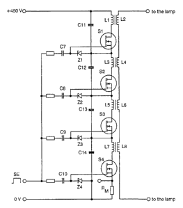
Figure 1 shows a series circuit of four class E converter
modules in a ballast for the purpose of supplying a
dielectrically impeded discharge lamp. A first module, which is
depicted at the top in figure 1 and is at a high potential, has
a switching transistor S1, here a power MOSFET, a storage
inductor L1 with a secondary winding L2, a supply electrolytic
capacitor 11, a drive coupling capacitor C7 and a zener diode
Z1. The storage inductor L1 and the switching transistor S1 are
connected in series, the source terminal of the switching
transistor S1 being at the bottom at the reference potential
CA 02521553 2005-09-28
- 8 - 2004P10255US-PAU
inside the module, which forms the positive supply potential of
the module (S2, L3, L4, C12, C8, Z2) situated therebelow.
The drain terminal of the switching transistor S1 is coupled to
the lower terminal of the storage inductor L1, whose upper
terminal is at an intermediate circuit DC voltage of
approximately 450 V. This intermediate circuit supply voltage
is generated in an inherently conventional way - not
illustrated here in detail - by rectification and conversion
with the aid of a step-up converter from a line supply voltage.
Lying in parallel with the series circuit composed of the
storage inductor L1 and the switching transistor S1 is the
supply capacitor C11 which serves to support the supply voltage
and is therefore designed as a relatively large electrolytic
capacitor.
A central control signal SE is fed in at bottom left in
figure 1 and is illustrated here symbolically as a square-wave
shape. This is applied, via resistors (not numbered) and drive
coupling capacitors C7-C10, in the case of the upper module C7,
to the gates of the switching transistors. Thus, the control
signal is coupled in in terms purely of AC voltage. Connected
between the gate terminal of the switching transistor S1 and
the source terminal is a zener diode Z1 that adjusts the DC
voltage level of the coupling capacitor C7 and prevents
overvoltages at the gate terminal. In addition, by skillfully
setting the incoupled drive signal level it is possible to
achieve that in the case of an opening of the switching
transistor S1 the drive signal is somewhat above the on-state
voltage of the zener diode Z1, thus causing short circuiting of
interference in the zener diode Z1 that is superposed on the
drive signal. The resistors in the common drive line, that is
to say the resistor to the left of the coupling capacitor C7,
for example, are provided for this short circuit situation.
CA 02521553 2005-09-28
- 9 - 2004P10255US-PAU
Located below the first module described is a second module of
identical design and having components numbered in a
correspondingly higher fashion, the internal (lower) reference
potential of the first module forming the positive supply
potential of the second module. Corresponding relationships
hold for the second and third module and for the third and
fourth module. As shown in figure 1, the internal reference
potential of the fourth module is at frame potential, and is
coupled to frame via a shunt RM in the case of the source
terminal of the fourth switching transistor S4.
As in the case of a voltage divider circuit, the supply voltage
of 450 V is distributed over the four supply capacitors C11-C14
such that each of the capacitors is charged to approximately
112.5 V. This is regarded as a favorable value because DC
voltages in the range between 40 V and 120 V are typically
favorable for operating class E converters used in operating
dielectrically impeded discharge lamps. The individual module
supply voltage could also be reduced by an appropriately higher
number of modules.
There was a certain fear at first that material tolerances, in
particular differing capacitances of the electrolytic
capacitors C11-C14 and/or different inductances, would lead to
substantially differing supply voltages of the individual
modules as far as destruction of the components. However, it
emerged that the fluctuations occurring are relatively slight
and manageable, and that the circuit behaves in a stable
fashion. The reason for this, in this instance, is that when an
individual module supply voltage is raised the pulse energy
converted by this module rises, and the corresponding supply
capacitor is thereby discharged more strongly.
Moreover, in the case of the circuit illustrated in figure 1 it
is not the drain-source voltages of the individual switching
transistors S1-S4 that are added together. Rather, the
individual drain-source voltage is added to the respective DC
CA 02521553 2005-09-28
- 10 - 2004P10255US-PAU
voltage level "therebelow" with reference to the circuit
reference point, that is to say, for example, the drain-source
voltage of the switching transistor S2 is added to the 225 V at
the upper terminal of the capacitor C13. Thus, what is involved
here is not a series circuit of individual switching
transistors such as is known, for example, for the purpose of
raising the total off-state voltage.
In addition to the voltage stabilization, the supply capacitors
C11-C14 are also intended to absorb energy fed back from the
secondary circuit into the primary circuit of the individual
class E converter module. Reference is made to US 6,323,600 B1
already cited. Otherwise, the mode of operation of class E
converters is known to the person skilled in the art.
In this exemplary embodiment, the storage inductors are coupled
to secondary windings L2, L4, L6 and L8 that form a series
circuit, in turn. Thus, inductive voltages on the secondary
side are also added together by the driving of the switching
transistors S1-S4, which is temporally synchronized in
accordance with figure 1.
The secondary-side inductors L2, L4, L6 and L8 could, of
course, also be interconnected differently, for example they
could be connected in parallel. This is a question of matching
the impedance to the dielectrically impeded discharge lamp to
be supplied. A series circuit is favorable in the present case,
because the aim is to generate relatively high voltages. The
serial output circuit is preferred chiefly because in the case
of parallel circuits manufacturing tolerances can cause the
flow of compensation currents which are disadvantageous with
regard to the electromagnetic compatibility and to losses
(so-called ringing . The powers of the individual modules add
together in each case to form a total power.
The invention also has the further advantage in this case that
more favorable design sizes, in particular design heights, can
CA 02521553 2005-09-28
- 11 - 2004P10255US-PAU
be attained in conjunction with relatively large required input
powers of the lamp to be supplied owing to the distribution
over a number of modules, in particular the distribution over a
number of inductors and/or transformers. A number of small
transformers are frequently more favorable in terms of design
than a relatively large one.
Figure 2 shows a variant of figure 1.
Figure 2 shows largely similar structures to that of figure 1,
the same reference symbols also having been used for
corresponding components. In addition, each module respectively
includes between the upper terminal of the zener diode and the
gate terminal of the switching transistor a rectifier diode
connected with its anode to the cathode of the zener diode, and
a bipolar transistor whose emitter is connected between this
rectifier diode and the gate terminal, whose base is connected
between the rectifier diode and the zener diode, and whose
collector is connected to the source terminal of the respective
switching transistor. The rectifier diodes are denoted by
D1-D4, whereas the bipolar transistors are denoted by S5-S8.
This interconnection ensures that the switching transistors
S1-S4 can be switched off particularly quickly by guiding the
potential at the gate terminal below the gate voltage threshold
value particularly quickly via the emitter-collector path of
the respective bipolar transistor S1-S8. The diodes Dl-D4
ensure that the switching transistors S1-54 can be switched off
via the bipolar transistors S5-S8 and can be switched on via
the diodes D1-D4.
Furthermore, the resistors denoted by Rl-R4 and which are in
parallel with the zener diodes ensure that the entire series
circuit of the class E converter modules switches off
automatically without a drive signal SE.
Figure 3 shows a third exemplary embodiment which differs from
the two previous exemplary embodiments firstly in that only
CA 02521553 2005-09-28
- 12 - 2004P10255US-PAU
three modules are used. Furthermore, here the primary and
secondary windings of the transformers Ll and L2, L3 and L4, L5
and L6 are drawn separately from one another, this being
intended only to serve clarity in the figure and not signifying
any technical changes as against figures 1 and 2. Finally, the
driving of the switching transistors Sl-S3, which is performed
in accordance with figure 2, is omitted here.
Firstly, additional capacitors C1, C3 and CS are respectively
provided in parallel with the switching transistors S1, S2 and
S3, which serve for signal shaping via the transistors. The
rectifier diodes D1-D3 depicted in parallel therewith
constitute the intrinsic body diodes of the switching
transistors S1-S3. When use is made not of MOSFETs but of
bipolar transistors, for example, it would then be necessary
for such separate diodes to be used.
Furthermore, taps are short circuited between the storage
inductors L1, L3 and L5 and the respectively associated
switching transistors S1, S2 and S3 via coupling capacitors C2,
C9 and C6. This high-frequency short circuit balances the AC
voltage signals and thereby guards against problems that can
occur because of the secondary voltage distribution and
capacitive couplings.
Finally, figure 4 shows a fourth exemplary embodiment, which
corresponds to the third exemplary embodiment from figure 3
with the following exception: the supply capacitors C11, C12
and C13 of the individual class E converter modules are
replaced by a single supply capacitor C21 that is situated in
parallel with the entire series circuit. Such a large
electrolytic capacitor is generally more cost effective than a
number of small ones.
An advantageous embodiment can also consist in a combination of
figures 3 and 4 to the effect that a relatively large common
storage capacitor C21 is used together with relatively small
CA 02521553 2005-09-28
- 13 - 2004P10255US-PAU
storage capacitors C11, C12 and C13 in the individual modules,
that is to say a total of four capacitors for the present three
modules. Because of the component costs, this solution would be
even more favorable than the solution in accordance with
figures 1-3, which is based exclusively on the individual
modules. In particular, foil capacitors can be used for the
storage capacitors of the individual modules.
Overall, the invention shows a high degree of flexibility owing
to a simple modular design by virtue of the fact that optimized
class E converter modules can be assembled depending on the
available DC voltage supply. It is possible to undertake
matching to the lamp to be supplied on the secondary side as
well by means of suitable interconnection (in serial or
parallel terms). The necessity for an interposed further
converter in order to reduce the DC voltage level of the output
of the step-up converter is eliminated. Instead of this, the
converter circuit in accordance with figures 1-4 can be
operated directly at the output of the step-up converter.
Finally, the division into a number of storage inductors and/or
transformers also offers a large degree of spatial flexibility
in the individual case, in particular a favorable design
height.
The invention is particularly suitable for supplying
dielectrically impeded discharge lamps, for example for
backlighting of monitors, specifically particularly in the case
of relatively high lamp powers (for example in the case of
large-format TV screens).