Note: Descriptions are shown in the official language in which they were submitted.
CA 02521675 2005-09-29
- 1 -
OR File No. 14774-20CA
METHOD OF PREPARING AN INTEGRATED CIRCUIT DIE
FOR IMAGING
TECHNICAL FIELD
The invention relates in general to examination and
analysis of integrated circuits and, in particular, to
methods of preparing an integrated circuit die for imaging
to permit a structure and layout of the integrated circuit
to be extracted.
BACKGROUND OF THE INVENTION
As is well known in the art, the examination and
analysis of integrated circuits requires sophisticated
sample preparation techniques and imaging tools. In the
past, integrated circuits were generally constructed using
aluminum for metal lines in each of the metal layers of the
integrated circuit and tungsten for vias interconnecting
the metal lines with components formed on a polycrystalline
silicon layer. Since aluminum and tungsten can be
selectively etched, integrated circuits could be
deconstructed using selective etching techniques that
permit the vias to be segregated from the metal lines, as
will be explained below in more detail with reference to
Fig. 1. Furthermore, modern integrated circuits generally
require sophisticated imaging equipments such as a scanning
electron microscope because components are frequently too
small to be visible under an optical microscope. In order
to distinguish vias from metal lines, it is therefore
necessary to acquire images that show contrast between the
vias and the metal lines. Tungsten and aluminum are
readily distinguished in scanning electron microscope
images.
CA 02521675 2005-09-29
- 2 -
OR File No. 14774-20CA
Consequently, a prior art technique illustrated in
Figs. 1a-1d for preparing an integrated circuit die for
imaging is commonly used to acquire tile images of a
deconstructed area of interest of an integrated circuit
die. Fig. 1a is a schematic cross sectional diagram of two
metal layers of an integrated circuit die generally
indicated by the reference 10. As is well known in the
art, each metal layer is covered by an interlayer
dielectric (ILD) 12 of a suitable material well known in
the art. A metal layer N+1 is separated from the
interlayer dielectric 18 on which it is deposited by a
barrier layer 16, also composed of a suitable material well
known in the art. The barrier layers 16, 22 prevent the
deposited metal layers N+1, N from migrating into the
interlayer dielectric 18, 24 onto which they are deposited.
A metal line 14 of metal layer N+1 is connected to a metal
line 20 of metal layer N by a via 26, which is also formed
in a manner well known in the art. The barrier layer 16
that separates via 26 from metal layer N is conductive and
provides an electrical connection between the via 26 and
the metal line 20.
In order to acquire tile images of the integrated
circuit 10, passivation layer 12, and any optional barrier
material (Fig. 1a) is first removed using a wet or dry
etching process or a chemical and/or mechanical polishing
process to expose metal lines 14 of metal layer N+1. The
integrated circuit die 10 is then placed on a precision
stage of the imaging equipment, a scanning electron
microscope for example, and tile images are acquired of the
area of interest in a manner well known in the art. After
the tile images of metal layer N+1 have been acquired, the
metal layer N+1 is removed using, for example, a wet or dry
etching process or a chemical and/or mechanical polishing
CA 02521675 2005-09-29
- 3 -
OR File No. 14774-20CA
process. The process is controlled to remove the metal
layer N+1 while preserving the integrity of the vias 26, as
shown in Fig. 1c. Thereafter, an etching solution is
selected that will remove the barrier layer 16 as well as
the interlayer dielectric 18 while leaving the via 26
intact. The results of that etching step are shown
schematically in Fig. 1d. If the etching is carefully
controlled, the via 26 remains intact and portions of the
barrier layer 16r that are shielded by the via 26 and
surround the via 26 remain after etching is complete. Thus
metal lines 20 of metal layer N and the via 26 are exposed
and tile images of the exposed via 26 and metal layer N are
acquired in a manner well known in the art.
This prior art process can be referred to as a "bottom
up" process because the vias are imaged in conjunction with
the metal lines to which they are connected at their bottom
ends. While this prior art technique works well for
integrated circuits constructed using aluminum metal lines
and tungsten vias due to the different etching
characteristics of the two metals, integrated circuits are
now being manufactured using copper metal lines and copper
vias. This makes the prior art method very difficult to
perform and complicates layout extraction, as will be
explained below with reference to FIG. 2.
FIG. 2 is a reproduction of an image of a copper
damascene integrated circuit prepared using the prior art
process described above with reference to FIGs 1a-1d. The
image 30 was acquired using a scanning electron microscope.
The integrated circuit die was prepared for imaging using a
controlled etching process that removed the metal lines of
metal layer N+1 and the interlayer dielectric 18 while
leaving, to an extent possible, the vias 26. As can be
CA 02521675 2005-09-29
- 4 -
OR File No. 14774-20CA
understood by those skilled in the art, the etching process
is difficult to control when the vias and the metal lines
are made of the same metal. Consequently, some of the vias
26 are eroded and have an oblong shape in the image. As
well, the copper lines 32 and the vias 26 are very similar
in shade and it is not consistently clear to which metal
line 32 a via 26 is connected. Circuit layout information
is therefore difficult to extract and prone to errors.
There therefore exists a need for a method of
preparing an integrated circuit die for imaging to permit a
structure and layout of the integrated circuit to be
extracted, regardless of metals used to construct the
integrated circuit.
SUN~lARY OF THE INVENTION
It is therefore an object of the invention to provide
methods of preparing an integrated circuit die for imaging
that permits a structure and layout of the integrated
circuit to be reliably extracted.
In accordance with one aspect of the present invention
there is provided a method of preparing an integrated
circuit die for imaging, comprising: removing interlayer
dielectric material from a metal layer of the integrated
circuit die to expose the metal layer; and removing all
metal from metal lines of the metal layer without removing
a barrier layer that underlies each metal line.
In accordance with another aspect of the present
invention there is provided a method for extracting circuit
information from an integrated circuit die, comprising:
removing all material covering a first metal layer of the
integrated circuit die; etching away all metal from the
first layer to completely expose a barrier layer underlying
CA 02521675 2005-09-29
- 5 -
OR File No. 14774-20CA
each metal line in the first metal layer; placing the
integrated circuit die on a precision stage and acquiring
tile images of an area of interest of the integrated
circuit die; repeating the removing, etching and placing
for each other metal layer; and removing an interlayer
dielectric material covering a polycrystalline silicon
layer of the integrated circuit die, placing the integrated
circuit die on the precision stage and acquiring tile
images of polycrystalline silicon layer.
In accordance with yet another aspect of the present
invention there is provided a method of preparing an
integrated circuit for imaging for the purpose of
extracting circuit information, comprising removing all
material including all metal from the metal lines and metal
vias of a metal layer of the integrated circuit die, and
acquiring tile images of barrier Layers exposed after all
of the metal has been removed from the metal lines and the
metal vias of the metal layer.
BRIEF DESCRIPTION OF THE DRAWINGS
Further features and advantages of the present
invention will become apparent from the following detailed
description, taken in combination with the appended
drawings, in which:
Figs. 1a-1d are schematic diagrams illustrating a
technique for preparing an integrated circuit die for
imaging in accordance with the prior art;
Fig. 2 is a reproduction of an image of a copper
damascene integrated circuit prepared using the method
shown in Figs. 1a-1d;
CA 02521675 2005-09-29
- 6 -
OR File No. 14774-20CA
Fig. 3 is a flow chart providing a high level overview
of methods for preparing an integrated circuit die for
imaging in accordance with the invention;
Figs. 4a-4d are schematic diagrams illustrating a
process for preparing an integrated circuit die for imaging
in accordance with the invention;
Fig. 5 is a reproduction of an image of an integrated
circuit prepared in accordance with a process illustrated
in Figs. 4a-4c; and
Fig. 6 is a reproduction of an image of an integrated
circuit prepared in accordance with a process illustrated
in Figs 4a, 4b and 4d.
It will be noted that throughout the appended
drawings, like features are identified by like reference
numerals.
DETAILED DESCRIPTION OF THE PREFERRED EMBODIMENT
The invention provides methods of preparing an
integrated circuit die for imaging that is useful for
preparing integrated circuit dies constructed using any
process in which both the metal lines and vias of the
integrated circuit are made of the same metal. The methods
are very useful for integrated circuits made using an all-
copper or an all-aluminum process. However, the process is
equally useful for preparing traditional aluminum/tungsten
integrated circuits for imaging. In accordance with the
method, after a metal layer of an integrated circuit is
exposed, all the metal lines in the metal layer are etched
away leaving behind barrier layer material. When images
are acquired using a scanning electron microscope, the
barrier layer material appears as a first color, typically
CA 02521675 2005-09-29
- 7 _
OR File No. 14774-20CA
light grey. If the chip is a copper/copper or
aluminum/aluminum construction, etching away the metal
lines likewise etches away the vias, leaving a barrier
layer that surrounds each via. When imaged, etched away
vias appear in a contrasting color, i.e. dark grey or
black. The contrasting colors permit feature extraction
software and/or an engineer analyst to readily discriminate
between the barrier layer material for the metal lines and
the barrier material lining cavities previously occupied by
the metal vial.
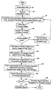
Fig. 3 is a flow chart providing a high level overview
of the methods in accordance with the invention. As is
well understood in the art, before an integrated circuit
die can be imaged it must be de-capsulated from a package
(step 40). After the integrated circuit die is de-
capsulated, a passivation layer 42 covering the first metal
layer (metal layer N+1) is removed (step 42), as shown in
Fig. 4b. The passivation layer may be removed using an
etching process well known in the art.
The integrated circuit is then subjected to a wet or
dry etching process to etch away metal lines 14 and vias 26
in order to expose an underlying barrier layer 16 (step
44). After the metal lines 14 and vias 26 are etched away
(see FIG. 4c), the chip is placed on a precision stage
(step 46) and tile images (step 48) are acquired of any
area of interest. It is then determined (step 50) whether
another metal layer of the integrated circuit exits. If
so, an interlayer dielectric (ILD) 18 and any barrier
material (not shown) that covers the metal lines is also
removed. As is understood by those skilled in the art, a
barrier layer is always applied under metal lines but the
barrier layer is not always applied over the metal lines.
CA 02521675 2005-09-29
_ g _
OR File No. 14774-20CA
Nonetheless, any process used to remove a passivation layer
or an ILD will also remove any barrier material covering
metal lines, while leaving the metal lines and any barrier
material underlying them. When all material has been
removed from that metal layer 20 (step 52), the process
branches back to step 44.
After all metal layers have been exposed, etched away
and imaged, any remaining interlayer dialectic is removed
and the die is once again placed on the precision stage and
images are acquired of a polycrystalline layer on which
circuit components are formed (step 54). The tile images
for each layer are stitched together in a manner well known
in the art (step 56) to form image mosaics. The image
mosaics are then vertically aligned, typically using via
connections between layers to ensure correct inter-mosaic
alignment (step 58). The aligned image mosaics are then
passed to a feature extraction algorithm to reconstruct a
parametric representation of the circuit die based on the
aligned mosaic images (step 60). Circuit information is
then extracted from the parametric representation
(step 62), and it is determined whether logical errors
exist in the circuit information (step 64). If so, a
report with error exceptions is generated. The report
including the error exceptions is passed to engineer
analysts who must study the image mosaics and correct any
missing or incorrect connections based on information
retrieved from the mosaic images. If no errors were
detected a report without error exceptions is generated
(step 68) and the process ends.
Figs. 4a-4c illustrate the process described above
with reference to Fig. 3 for an integrated circuit
constructed using a copper damascene process. The
CA 02521675 2005-09-29
- 9 -
OR File No. 14774-20CA
integrated circuit 10 shown in Fig. 4a includes an
passivation layer 12 that covers metal lines 14 of metal
layer N+1 . A via 2 6 interconnects the metal line 14 with
the metal line 20 in the metal layer N. A barrier layer 16
segregates the metal line 14 from interlayer dielectric
material 18. Barrier layer 16 is conductive and provides a
connection between via 26 and metal line 20 of metal layer
N. A barrier layer 22 separates metal line 20 from the
interlayer dielectric 24 to ensure that no metal migrates
into the interlayer dielectric, which would change its
properties. As explained above, a barrier material (not
shown) is applied over metal lines in some integrated
circuit manufacturing processes.
Fig. 4b shows the integrated circuit die 10 after the
passivation layer material 12 has been removed from the
metal lines 14 of metal layer N+1. A wet or dry etching
process is then used to etch away the metal lines 14 and
the vias 26 leaving the barrier layer 16 shown in Fig. 4c.
The integrated circuit shown in Fig. 4c is then ready for
imaging.
As will be appreciated by those skilled in the art,
the methods in accordance with the invention produce images
in which vias 26 are shown in conjunction with the metal
lines 14 to which they are connected at a top end, which is
opposite to the methods used in the prior art. The process
can therefore by described as a "top down" process. As
will further be appreciated by those skilled in the art,
layout extraction algorithms may require adjustment to
ensure proper layout extraction using mosaic images
acquired using integrated circuit die preparation methods
in accordance with the invention.
CA 02521675 2005-09-29
- 10 -
OR File No. 14774-20CA
Fig. 5 is a reproduction of an image of a
copper/copper integrated circuit prepared for imaging using
the process shown in Figs. 4a-4c. The image 80 is a
scanning electron microscope image of an area of interest
of the integrated circuit die. The barrier layers 82 that
underlaid metal lines of the integrated circuit are light
grey. The barrier layers that underlaid the vias 84 are
dark grey or black, and are easily distinguishable from the
barrier layers that underlaid the etched-away metal lines.
The vias are also well defined and there is no ambiguity
about the metal line with which each via is associated.
Since the barrier layers that underlaid the vias are easily
distinguished from the barrier layers that underlaid the
metal lines, automated layout extraction is very efficient
and completes with an extremely low error rate.
Fig. 4d shows the integrated circuit 10 prepared in
accordance with the invention when the integrated circuit
is constructed using aluminum lines 14 and tungsten vias
26. When that is the case, the etching processes shown in
FIGS. 4a and 4b removes the aluminum lines but leaves the
tungsten vias 26, as shown in Fig. 4d.
Fig. 6 is a reproduction of an image of an area of
interest of an integrated circuit constructed with aluminum
lines and tungsten vias prepared for imaging in accordance
with the invention. The image 90 was acquired using a
scanning electron microscope. The barrier layers 92 appear
as light grey lines while the tungsten vias 94 appear as
bright white spots. Once again, feature extractions
software is readily able to distinguish between background,
the barrier layers 92 and the vias 94. Feature extractions
is therefore facilitated and automated layout extraction
errors are significantly reduced.
CA 02521675 2005-09-29
- 11 -
OR File No. 14774-20CA
The invention therefore provides a less time
consuming, simpler and more efficient method of preparing
an integrated circuit die for imaging. The process
provides images with better contrast and is particularly
well adapted to use with integrated circuits manufactured
using a copper damascene process, although it provides
excellent results when used with any known integrated
circuit construction.
The embodiments of the invention described above are
intended to be exemplary only. The scope of the invention
is therefore intended to be limited solely by the scope of
the appended claims.