Note: Descriptions are shown in the official language in which they were submitted.
CA 02521739 2005-09-30
Chen 2-6-37-1-5
INPHASE/QUADRATURE PHASE IMBALANCE COMPENSATION
BACKGROUND
Field of the Invention
The invention relates generally to quadrature-modulation and relates more
particularly to methods and apparatus for compensating inphase/quadrature
phase
imbalance in transceivers.
Discussion of the Related Art
Some radio frequency (RF) transceivers provide direct or low intermediate
frequency (IF) conversion architectures in which single-stage quadrature-
modulation
is available without bulky analog filters. In these architectures, the
transceivers often
produce imbalances between the parallel signal streams that are associated
with
inphase (I) and quadrature phase (Q) components of modulated carriers. These
I/Q
imbalances can include amplitude and/or phase mismatches of about one to three
percent. Often, such I/Q imbalances result from errors related to the limited
tolerance
in the micro-fabrication of integrated circuits (ICs). Thus, I/Q imbalances
cannot
simply be eliminated from analog components of IC transceivers.
In an IC transceiver, digital signal processors (DSPs) can compensate I/Q
imbalances that are produced by analog circuits of the transceiver. Indeed,
DSP-
assisted I/Q compensators outperform analog counterparts and are often easy to
modify to enable circuit adaptation.
There are several types of DSP-assisted compensators for UQ imbalance. One
DSP-assisted I/Q compensator is configured to evaluate an 1/Q imbalance via
training
cycles and then, exploit an adaptive algorithm to compensate for the I/Q
imbalance.
Another DSP-assisted I/Q compensator has adaptive filters that compensate for
the
I/Q imbalance in a low IF receiver.
DSP-assisted 1/Q compensators may have several drawbacks. The possible
drawbacks include the incorporation of significant extra circuitry to collect
feedback
information, a lack of compensation for imperfections in the calibration
circuitry itself
and/or a reliance on off-line training. Thus, it is desirable to have other
methods and
apparatus for compensating 1/Q imbalances in quadrature-modulation
transceivers.
CA 02521739 2005-09-30
Chen 2-6-37-1-5
BRIEF SUMMARY
Various embodiments include transceivers that compensate 1/Q transceiver
imbalances by exploiting the duplex nature of the transceiver. The calibration
of I/Q
compensators involves coupling the output of the transmitter to the input of
the
receiver. The signal stream transmitted by the transmitter functions as a
training
stream for calibrating circuits for compensating hardware-induced I/Q
imbalances.
Thus, some of the new transceivers can calibrate I/Q compensation circuits
without
using off-line training cycles.
One embodiment features a transceiver that includes a transmitter, a receiver,
and an electrical feedback Line. The transmitter has a quadrature-modulator
and is
configurable to compensate inphase/quadrature phase imbalances produced by
hardware of the transmitter. The quadrature-modulator is configured to
quadrature-
modulate a carrier wave. The receiver has a quadrature-demodulator and is
configurable to compensate for inphase/quadrature phase imbalances produced by
hardware in the receiver. The quadrature-demodulator is configured to
demodulate a
quadrature-demodulated Garner. The electrical feedback line connects an output
of
the transmitter to an input of the receiver.
Another embodiment features a method of reducing inphase/quadrature phase
(I/Q) imbalances in a transceiver. The method includes updating a
configuration of
one or more 1/Q compensators of the transceiver to reduce a roundtrip I/Q
imbalance
between parallel signal streams that the transceiver quadrature-modulates onto
a
carrier wave and then, demodulates from the Garner wave.
Another embodiment features a transceiver that includes a transmitter, a
receiver, and an inphase/quadrature phase compensation controller. The
transmitter
has an inphase/quadrature phase digital compensator to produce, in parallel,
first and
second compensated digital signal streams from first and second input digital
signals
streams. The transmitter has an analog circuit for quadrature-modulating a
carrier
wave with said first and second compensated digital signal streams. The
receiver has
an analog circuit to produce, in parallel, first and second demodulated signal
streams
by demodulating a quadrature-modulated carrier. The receiver has an
inphase/quadrature phase digital compensator to produce, in parallel, third
and fourth
compensated output digital signal streams from the first and second
demodulated
CA 02521739 2005-09-30
Chen 2-6-37-1-5
signals streams. The inphase/quadrature phase compensation controller is
configured
to determine inphase/quadrature phase mismatches for signals that are both
quadrature-modulated by the transmitter and demodulated by the receiver.
BRIEF DESCRIPTION OF THE DRAWINGS
Figure 1 is a block diagram of a quadrature-modulation transceiver that
implements dynamical compensation of inphase/quadrature phase (1/Q) hardware
imbalances;
Figure 2 is a timing diagram for one method of operating the transceiver of
Figure 1;
Figure 3 is a block diagram showing analog (A) and digital (D) circuits in the
transceiver shown in Figure 1;
Figure 4A is a block diagram of one embodiment of analog processing lines of
the transmitter shown in Figure 3;
Figure 4B is a block diagram of one embodiment of analog processing lines of
the receiver shown in Figure 3;
Figure SA is a block diagram of one exemplary embodiment of the quadrature-
modulator in the transmitter shown in Figure 3;
Figure SB is a block diagram of one exemplary embodiment of the quadrature-
demodulator in the receiver shown in Figure 3;
Figure 6A is a block diagram of one embodiment of an 1/Q digital pre-
compensator of the transmitter shown in Figure 3;
Figure 6B is a block diagram of one embodiment of an I/Q digital post-
compensator of the receiver shown in Figure 3;
Figures 7A and 7B illustrate the two modes of a 2x2 switch in the receiver of
Figure 3;
Figure 8 is a flow chart illustrating a method of calibrating the I/Q pre-
compensator and I/Q post-compensator of the transceiver shown in Figure 3;
Figures 9A - 9E show the evolution of 1/Q gain imbalances as the method of
Figure 8 is performed for a first exemplary embodiment of the transceiver show
in
Figure 3; and
CA 02521739 2005-09-30
Chen 2-6-37-1-5
Figure 10 illustrates a simulation of the evolution of the I/Q compensating
gains and phases as the method of Figure 8 is performed for a second exemplary
embodiment of the transceiver show in Figure 3.
In the Figures and text, like reference numerals indicate elements with
similar
functions.
In the Figures and detailed description, various embodiments are described.
Nevertheless, the inventions may be embodied in various forms and are not
limited to
the embodiments described in the Figures and detailed description.
DETAILED DESCRIPTION OF ILLUSTRATIVE EMBODIMENTS
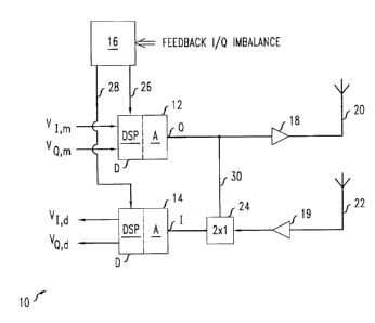
Figure 1 shows a transceiver 10 that implements a quadrature-modulation
scheme, e.g., quadrature phase shift keying or 16-phase shift keying with 4
and 16
signal-point constellations, respectively. The transceiver 10 includes a
transmitter 12,
a receiver 14, and an inphase/quadrature phase (1/Q) digital compensation
controller
16.
The transmitter 12 converts Vi,m and VQ,m digital baseband signal streams,
which are received in parallel, into modulations on inphase and quadrature
phase
components of a carrier wave, e.g., an RF wave. The conversion includes
processing
the parallel signal streams in digital (D) and analog (A) circuits. Due to
intrinsic
limitations of micro-fabrication tolerances and/or variations in operating
conditions,
the A circuit typically introduces I/Q imbalances, i.e., amplitude and/or
phase
imbalances, between corresponding signals of the two parallel signal streams.
The
transmitter 12 outputs a quadrature-modulated carrier wave at an output, O,
where a
power amplifier 18 amplifies the modulated carrier prior to transmission to a
channel,
e.g., via transmission antenna 20.
The receiver 14 converts a quadrature-modulated carrier wave, which is
received at input I into parallel VI,d and VQ,d digital baseband signal
streams. The
quadrature-modulated Garner is, e.g., received from reception antenna 22 via
another
low-noise amplifier 19 and a 2x1 switch 24. The conversion involves processing
parallel signal streams, which are produced from the quadrature-modulated
carrier,
with both A and D circuits. Due to intrinsic limitations of micro-fabrication
tolerances and/or variations in operating conditions, the A circuit typically
introduces
CA 02521739 2005-09-30
Chen 2-6-37-1-5
I/Q imbalances, i.e., amplitude and/or phase imbalances, between corresponding
ones
of the signals in the parallel signal streams.
The I/Q compensation controller 16 dynamically controls the transmitter 12
and receiver 14 with control signals transmitted via lines 26, 28. In
particular, the I/Q
compensation controller 16 calibrates DSPs, i.e., the D circuits, of both
transmitter 12
and receiver 14 so that the DSPs compensate both amplitude and phase I/Q
imbalances that are produced in the A circuit of each device. The I/Q
compensation
controller 16 dynamically adjusts the DSPs during calibration modes.
In each calibration mode, the 2x1 switch 24 connects electrical feedback line
30 between the output O of the transmitter 12 and the input I of the receiver
14 and
disconnects the reception antenna 22 from the input I. In the calibration
mode, the
I/Q compensation controller 16 iteratively adjusts the DSPs so that Vi,a /VQ,a
equals
VI,m~Q,m in both magnitude and phase. The calibration mode may be incorporated
into the standard duplex operation of the transceiver 10.
Figure 2 illustrates one method for incorporating calibration (Cal) modes into
the standard duplex operation, wherein the transceiver 10 interleaves
reception time
slots (Rx) and transmission time slots (Tx). During the Rx time slots, the
transmitter
12 remains idle so that wireless transmissions of the transceiver 10 do not
interfere
with the reception of wireless transmissions from other transceivers (not
shown). In
the Tx time slots, the receiver 14 does not however, remain idle. Instead, the
receiver
14 actively receives and processes the quadrature-modulated carrier
transmitted in the
Tx time slots. Indeed, this feedback quadrature-modulated carrier is used to
calibrate
the I/Q compensation circuits of the DSPs. The reception is preferably direct
between
the output O and input I to avoid nonlinear distortions in the amplifiers 18,
19.
Comparing the known input signal streams, i.e., VQ,m and Vi,m, to the two
parallel
signal streams, i.e., VQ,a and Vi,a, produced by the receiver 14 enables
determining
whether I/Q compensation is needed. Thus, the Tx time slots serve both for
transmission of communication to other transceivers and for calibration (Cal)
of the
digital I/Q compensation circuits of the transceiver 10 itself. For this
reason, extra
training cycles are not used to calibrate the circuits involved in
compensating I/Q
imbalances.
CA 02521739 2005-09-30
Chen 2-6-37-1-5
Whereas the A signal processing circuits of the transmitter 12 and receiver 12
generate I/Q imbalances, the 1/Q compensation controller 16 dynamically
calibrates
digital pre- and post- compensation to eliminate overall I/Q imbalances in
both
transmitter 12 and receiver 14.
In the method of Figure 2 and transceiver 10 of Figure 1, calibration of I/Q
compensation uses roundtrip pairs of signals, i.e., pairs of signals that are
first
quadrature-modulated in the transceiver's transmitter 12 and then, demodulated
in the
transceiver's receiver 14. For that reason, the calibration of the I/Q
compensation is
less susceptible to errors in circuitry that used to determine the I/Q
imbalances.
Figure 3 shows portions of the D and A circuits of the transmitter 12 and
receiver 14 of Figure 1.
In the transmitter 12, the A circuit includes first analog processing line 34
for
a first signal stream, parallel second analog processing line 36 for the
parallel second
signal stream, i.e., I and Q branches, and quadrature-modulator 38, and the D
circuit
includes digital I/Q pre-compensator 32. The first and second analog
processing lines
34, 36 independently process the signal streams produced from the input Vi,m
and
VQ,m digital baseband signal streams, respectively. Exemplary analog
processing
lines 34, 36 include a digital-to-analog (D/A) converter and a low pass (LP)
filter as
shown in Figure 4A. The quadrature-modulator 38 mixes the I and Q components
of
a carrier wave with the processed signal streams received from the respective
first and
second processing lines 34, 36 to produce a quadrature-modulated carrier at
output O.
An exemplary quadrature-modulator 38 includes a source (S) for the carrier
wave, a
90° phase shifter (PS), analog mixers (M's), and an analog combiner
(AC) as shown
in Figure SA. The digital I/Q pre-compensator 32 processes the input digital
baseband signal streams VI,m and VQ,m to pre-compensate for I/Q imbalances
that will
be produced in the analog first and second processing lines 34, 36 and the
analog
quadrature-modulator 38.
In the receiver 12, the A circuit includes quadrature-demodulator 50, first
analog processing line 46, and parallel second analog processing line 48,
i.e., I and Q
branches, and the D circuits includes 2x2 switch 44 and I/Q post-compensator
42.
The quadrature-demodulator 50 mixes a received signal with a carrier wave to
produce from the signal's I component and Q component two parallel signal
streams
CA 02521739 2005-09-30
Chen 2-6-37-1-5
at the baseband or at an intermediate frequency range. An exemplary quadrature-
demodulator 50 includes a source (S) for the carrier wave, a 90° phase
shifter (PS),
and analog mixers (M's) as shown in Figure SB. The analog processing lines 46,
48
perform independent processing of the two parallel signal streams that are
produced
by the quadrature-demodulator 50. Exemplary analog processing lines 46, 48
include
a LP filter, e.g., to recover the baseband, and an analog-to-digital (A/D)
converter as
shown in Figure 4B. The I/Q digital post-compensator 42 processes the parallel
baseband digital signal streams to dynamically compensate for I/Q imbalances,
i.e.,
amplitude and/or phase imbalances generated in the processing lines 46, 48 and
quadrature-demodulator 50. The 2x2 switch 44 enables controllably exchanging
the
two signal streams from the analog processing lines 46, 48 to provide for two
connection modes, i.e., modes A and B.
Figures 6A and 6B illustrate exemplary embodiments of the I/Q digital pre-
compensator 32 and the I/Q digital post-compensator 42, respectively.
Referring to Figure 6A, the I/Q pre-compensator 32 includes a digital
multiplier 52; a digital multiplier 54, and a digital adder 56. The digital
multiplier 52
has a controllable multiplier factor of tan(~m~) on one input, i.e., a gain
factor, and the
digital multiplier 54 has a controllable multiplier factor of 1/[gm~cos(~m~)]
on one
input, i.e., a gain factor. Here, gm~ and ~m~ are parameters are set
dynamically and
iteratively by the I/Q compensation controller 16 based on fed back gain
ratios and
phase differences for VQ,m and Vi,m and for VQ,d and VI,a. The
tan(~~,°) and
1/[gm~cos(~m~)] gain factors of the digital multipliers 52, 54 are set by
control signals
received via line 26. The I/Q digital pre-compensator 32 compensates an A
circuit of
the transmitter 12 if the A circuit produces a gain imbalance of gm~ and a
phase
imbalance of ~m~ between the two parallel signal streams that quadrature-
modulate the
I and Q components of the Garner wave.
Referring to Figure 6B, the I/Q post-compensator 42 includes a digital
multiplier 58, a digital multiplier 60, and a digital adder 62. The digital
multiplier 58
has a controllable multiplier factor of tan(~d~) on one input, i.e., a gain
factor, and the
digital multiplier 60 has a controllable multiplier factor of 1/[gd~cos(~d~)]
on one
input, i.e., a gain factor. Again, gds and ~d~ are parameters that are set
dynamically
CA 02521739 2005-09-30
Chen 2-6-37-1-5
and iteratively by the I/Q compensation controller 16 based on fed back gain
ratios
and phase differences for VQ,m and Vi,m and for VQ,a and V~,a. The tan(~a~)
and
1/[ga~cos(~a~)] gain factors of the digital multipliers 58, 60 are set by
control signals
received via line 28. The I/Q digital post-compensator 42 will compensate an A
S circuit of the receiver 14 if the A circuit produces a gain imbalance of gm~
and a phase
imbalance of ~r"~ between the two parallel signal streams made by quadrature-
demodulating the I and Q components of a carrier wave.
Referring to Figures 7A - 7B, the 2x2 switch 44 has inputs 1, 2 and outputs 3,
4. The switch 44 electrically connects the receiver's analog processing lines
46, 48 to
the inputs of the I/Q post-compensator 42 in one of two modes. In mode A, the
inputs
1, 2 connect to the outputs 3, 4 via the uncrossed configuration shown in
Figure 7A.
In mode B, the inputs 1, 2 connect to the outputs 3, 4 via the crossed
configuration
show in Figure 7B. In mode B, one of the connection lines of the switch 44 may
include a digital inverter (INV). At the inputs of the I/Q post-compensator
42, such a
single inverter INV will effectively cause an equivalent transformation of ~a~
-~ - Sao,
wherein ~a~ is the phase parameter for the I/Q post-compensator 42. The switch
44
switches between the modes A and B in a manner that is responsive to control
signals
received via the line 28 from the I/Q compensation controller 16.
In other embodiments, the 2x2 digital switch 44 is replaced by an analog
switch in the A circuit of the receiver 14. Then, the analog switch (not
shown) would
serially connect the input of the analog processing line 46 to one output the
quadrature-demodulator 50 and would serially connect the input of the other
analog
processing line 48 to the other output of the quadrature-demodulator 50.
Again, the
crossed or B mode of such a switch typically could have an inverter on one of
the
internal lines of the switch.
Referring to Figures 1 and 3, the I/Q digital compensation controller 16
dynamically updates configurations of the I/Q pre-compensator 32 and the I/Q
post-
compensator 42 during calibration time slots, e.g., as shown in Figure 2. Each
update
is based on a set of corresponding signal values from the VI,m, VQ,m, VI,d,
and VQ,a
digital signal streams. The sets of corresponding digital signal values are
fed back to
the UQ digital compensation controller 16 via lines 64, 65, 66, 67. Herein, at
cycle k,
CA 02521739 2005-09-30
Chen 2-6-37-1-5
a corresponding set { Vi,a(k), VQ,a(k), VI,m(k), VQ,m(k) }includes the input
VI,m(k) and
VQ,m(k) digital baseband signals for signal cycle "k" and the output VI,a(k)
and VQ,a(k)
digital baseband signals that are produced by demodulation in the receiver 14
of a
carrier wave that was quadrature-modulated with the baseband V~,m(k) and
VQ,m(k)
signals. Performing this demodulation includes connecting the feedback line 30
between the output O of the transmitter 12 and the input I of the receiver 14
and
setting the 2x2 switch 44 to mode A or B. That is, the signal set { VI,a(k),
VQ,a(k),
VI,m(k), VQ,m(k) } is associated with a roundtrip of a pair of signals through
the
transmitter 12 and receiver 14 of the same transceiver 10. From each such
corresponding set of signals VI,a(k), VQ,a(k), Vl,m(k), and VQ,m(k), the 1/Q
digital
compensation controller 16 is configured to generate a corresponding amplitude
and
error signal, eg(k), and a corresponding phase error signal, e~(k). Exemplary
expressions for these error signals are:
a (k) - VI,m (k) / VQ,m (k) _ 1
g
V~,a (k) / VQ,a (k)
e~(k)=arg{VLm(k)+iVQ,m(k)}-sin-' VQ.a(k)~',.m(k)
V,,a (k) ~ V,,m (k) + iVQ,m (k) ~
From the corresponding error signals eg(k) and e~(k), the I/Q digital
compensation
controller 16 is configured to generate an iterative update of the parameters
gm~(k),
ga~(k), ~m~(k), and ~a~(k) that define the processing properties of the I/Q
pre-
compensator 32 and the I/Q post-compensator 42 at cycle "k". An update
replaces the
cycle-k parameter values gm~(k), gd~(k), ~mc(k), and ~a~(k) by updated cycle-
(k+1 )
parameter values gm~(k+1), gd~(k+1), ~m~(k+1), and ~a~(k+1), respectively. An
exemplary relationship between the updated and original parameters may, e.g.,
have
the following form:
g~~(k +1) = g,~~(k)[1 +~tgeg (k)],
ga~(k+1) =ga~(k)[l+p&e~(k)],
~m~(k+1) _ $myk)+p~em(k),and
~a~ (k + 1) _ ~a~ (k) + !-~~e~ (k)~
CA 02521739 2005-09-30
Chen 2-6-37-1-5 10
Here, ~g andp~ are step-sizes defining how the parameters gm~(k), ga~(k),
~mc(k), and
~a~(k) are incremented over a single update cycle. The above exemplary
relationships
provide an update operation that rescales gm~(k) and gd~(k) by an equal amount
over a
single update cycle and that shift ~",~(k) and ~a~(k) by an equal amount over
a single
update cycle. During calibration time slots, the I/Q compensation controller
1G
iteratively updates the parameters for the I/Q pre-compensator 32 and the I/Q
post-
compensator 42 in a manner that reduces overall I/Q imbalances in both the
transmitter 12 and the receiver 14.
In other embodiments of the transceiver 10, the e~(k) and e~(k) error signals
of
the above update relations may be implemented to have other forms. For
example, an
one form for the phase error signal, e~(k), is given by:
eø(k) _ ~~hd(k) - ~Q,d(k)~ - ~~I,m(k) - ~Q,m(k)~
Here, ~lI,d(k), ~Q,d(k), y,m(k), and ~Q,m(k) are the phases of VI,d(k),
VQ,d(k), Vi,m(k), and
VQ,~,(k), respectively.
Figure 8 illustrates one embodiment of a method 70 for calibrating the I/Q
compensators 32, 42 of the transceiver 10 of Figures 1 and 3 so as to provide
compensation of the I/Q imbalances in both the transmitter 12 and the receiver
14.
The method 70 includes initializing the parameters that define the properties
of the I/Q digital compensators 32, 42 (step 72). Exemplary initial values
satisfy:
gm~(k) = ga~(k) = 1 and ~m~(0) _ ~a~(0) = 0. Other initializations of these
parameters
are also possible in the method 70, which should be fairly insensitive to the
specific
initialization.
The method 70 includes performing a set iterative update cycles of the
parameters defining the I/Q pre-compensator 32 and the I/Q post- compensator
42
while the switch 44 is kept in mode A (step 74). In each cycle k, the I/Q
compensation controller 16 updates the parameters gm~(k), ga~(k), ~mc(k), and
~a~(k) as
described in the above iterative update formulas. Each update involves
rescaling
gmc(k) and gd~(k) by equal multiplicative factors. Here, each multiplicative
factor
differs from one by a quantity proportional to the 1/Q amplitude imbalance
produced
by a roundtrip of a signal pair through the transceiver 10. Each update also
involves
shifting ~n,~(k) and ~d~(k) by the equal shift amounts. Here, each shift
amount is, at
CA 02521739 2005-09-30
Chen 2-6-37-1-5 il
least, roughly proportional to the I/Q phase imbalance produced by the
roundtrip of
signal pairs through the transceiver 10. The iterative updates stop either in
response
to the magnitudes of the eg(k) and e~(k) error signals being smaller than a
preselected
threshold value or in response to a preselected number of said iterative
updates having
been performed.
Next, the method 70 includes switching the 2x2 switch 44 to mode B and
appropriately transforming the parameters defining the I/Q digital post-
compensator
42 (step 76). In particular, the switch to mode B interchanges the two
parallel signal
streams output by the receiver's A circuit. Thus, the switch effectively
inverts the I/Q
gain imbalance produced by said receiver's A circuit and changes the sign of
the I/Q
phase imbalance produced by said receiver's A circuit. At step 76, an
appropriate
transformation on the parameters that define the I/Q digital post-compensator
42 is:
gac(p) ~ (gac(P)~~ and ~ac(P)'~ - $ac(p)
Here, p is the iterative update cycle number prior to the mode switch. Such a
transformation enables the method 70 to effectively apply different updates to
the I/Q
compensator 32 and the I/Q compensator 42 in subsequent steps thereby enabling
different I/Q compensations in the transmitter 12 and the receiver 14. Also,
this
transformation does not, e.g., change the overall I/Q balance of the
transceiver 10
when it is performed along with the mode change if both the transmitter 12 and
the
receiver 14 are completely UQ compensated.
Next, the method 70 includes performing a set iterative update cycles for the
parameters defining the 1/Q pre-compensator 32 and the I/Q post-compensator 42
while switch 44 is in mode B (step 78). In each cycle k, the I/Q compensation
controller 16 again updates the present values of parameters gmc(k), gac(k),
~c(k), and
~ac(k) according to the above-described iterative update equations. In
particular, each
update involves rescaling gmc(k) and ga~(k) by equal multiplicarive factors.
Here, each
factor differs from one by an amount proportional to the I/Q amplitude
imbalance
produced by a roundtrip of a signal pair through the transceiver 10.
Similarly, each
update involves shifting ~n,c(k) and ~ac(k) by the equal amounts. Here, each
shift
amount is, at least, roughly proportional to the I/Q phase imbalance produced
by a
roundtrip of a signal pair through the transceiver 10. The iterative updates
are
CA 02521739 2005-09-30
Chen 2-6-37-1-5 12
stopped either in response to magnitudes of the e~(k) and e~(k) error signals
being
smaller than a preselected threshold value or in response to having performed
a
preselected number of the iterative updates.
Next, the method 70 includes switching the 2x2 switch 44 back to mode A and
appropriately transforming the parameters defining the I/Q post-compensator 42
(step
80). The switch of mode effectively inverts the I/Q gain imbalance produced by
said
A circuits and changes the sign of the I/Q phase imbalance produced by said A
circuits. Here, the transformation is analogous to the transformation of step
76.
Thus, the appropriate transformation of I/Q compensation parameters is again:
ga~(P' ) '~ fga~(P' )~ 1 and ~a~(P' ) ~ - $a~(P' )~
Here, p' is the iterative update cycle prior to the mode switch. Again, such a
transformation does not change the overall UQ balance of the transceiver 10
when it is
performed along with the mode change if both the transmitter 12 and the
receiver 14
are completely I/Q compensated.
Next, the method 70 includes evaluating whether the magnitudes of error
signals e~(k) and e~(k) are below another preselected threshold in mode A
(step 82).
If the magnitudes of the error signals are below the threshold, the
calibrations of the
I/Q digital pre-compensator 32 and the I/Q post-compensator 42 are completed.
Otherwise, the method 70 may involve executing a loop 84 back to again perform
steps 74 - 82.
Example 1
Figures 9A-9E illustrate the method 70 for an exemplary embodiment of
transceiver 10. In the exemplary embodiment, the A circuit of the transmitter
12 has
an I/Q imbalance that is a pure gain, g-r, wherein gT = 2. Similarly, in the
exemplary
embodiment, the A circuit of the receiver 14 has an I/Q imbalance that is a
pure gain,
gR, wherein gR = 8. The method 70 evolves the gains g~~ and gay of the I/Q
digital
compensators 32, 42.
At step 72, the method 70 involves initializing the gain of both the I/Q pre-
compensator 32 and the 1/Q post-compensator 42 to one, i.e., g~,~(0) = ga~(0)
= 1 as in
Figure 9A. Thus, the roundtrip I/P gain imbalance, g, i.e., g =
~Vt,m(k)/VQ,d(k)I~
~Vi,a(k)/VQ,a(k)~, initially satisfies: g = 1x2x8x1 = 16.
CA 02521739 2005-09-30
Chen 2-6-37-1-5 13
At step 74, the method 70 involves iteratively rescaling the values of the
gains
of UQ compensators 32, 42 while switch 44 is in mode A. The above-described
iterative update formulas imply that each of the iterations will multiply the
gain of
both UQ compensators 32, 42 by the same factor. The iterative rescalings stop
after N
iterations in response to eg(N) = 0. Then, total roundtrip gain is one. This
implies that
gm~(N) = ga~(N) ~ 1/4 as in Figure 9B.
At step 76, the method 70 involves switching to mode B and appropriately
transforming the gain of the UQ post-compensator 42. Switching to mode B
effectively inverts the gain of the receiver's A circuit from 8 to 1/8. Thus,
the
appropriate transformation of the gain, gay, of the UQ post-compensator is the
inversion transformation that maps ga~(N) to [ga~(N)]~1 = 4 as in Figure 9C.
At step 78, the method 70 involves performing additional M iterative updates
of the gains of the UQ pre-compensator 32 and the UQ post-compensator 42,
wherein
the additional updates rescale the gains gm~ and gay by equal amounts and stop
when
ea(N+M) = 0. Due to the condition on eg(N+M), the updates stop when gm~ ='/z
and
gay = 8 as shown in Figure 9D. Here, M is the number of additional iterations.
At step 80, the method 70 involves switching from mode B back to mode A
and appropriately transforming the gain of the UQ post-compensator 42.
Switching to
mode A returns the gain of the receiver's A circuit to 8, which implies that
the
appropriate transformation of the gain of the UQ post-compensator 42 is: gds ~
[gds]-1
= 1/8 as shown in Figure 9E.
At step 82, the method 70 involves evaluating the new value of the gain error
e~(N+M). After step 80, the new value of the gain error is zero. For that
reason, the
calibration of the UQ compensators 32, 42 has been completed. The method 70
succeeded in completely compensating the UP gain imbalances in both the
transmitter
12 and the receiver 14.
Examine 2
Figure 10 shows a simulation of the evolution of the compensating UQ gains
and UQ phases in another transceiver when these imbalances were corrected by
the
method 70 of Figure 7. In the simulation, the A circuit of transmitter 12 has
an initial
UP gain of 1.02 and an initial UP phase of 2 degrees, and the A circuit of the
receiver
14 has an initial UP gain of 1.04 and an initial UP phase of 4 degrees. The
simulated
CA 02521739 2005-09-30
Chen 2-6-37-1-5 14
results of Figure 10 show that about 22 iterations in mode A and about 20
iterations in
mode B suffice to compensate the I/P imbalances of both the transmitter 12 and
receiver 14 for this exemplary embodiment. Thus, small I/Q imbalances can be
rapidly dynamically compensated.
Other embodiments of the inventions will be apparent to those of skill in the
art in light of the description, drawings and claims.