Note: Descriptions are shown in the official language in which they were submitted.
CA 02521878 2005-09-29
SELF-SHIELDED ELECTRONIC COMPONENTS
FIELD OF THE INVENTION
[0001] The present invention relates generally to electronic components. More
particularly,
the present invention relates to shielding of passive electronic components
such as inductors,
transformers and balun power combiners or balun power splitters.
BACKGROUND OF THE INVENTION
[0002] Future broadband wireless networks will utilize integrated circuits
that process radio
frequency (RF) signals in bands where wavelengths may be just a few
millimeters. For
example, operation in the 24 GHz ISM band reduces congestion in lower
frequency bands and
supports data services up to hundreds of megabytes per second (Mb/s), enabling
the next
generation of wireless access and connectivity. Efficiency of passive
electronic components is
paramount when operating at radio frequencies. This is also true at millimeter
wavelengths,
because the quality of electronic circuit realizations depends more upon low-
loss passive
components as the wavelength shrinks.
[0003] Implementation of a 24 GHz power amplifier in silicon technology, for
example, is
hindered by transmission line effects that change the behavior of the signals
being processed
considerably. Signal attenuation ranges between 0.5 and 2.0 dB/mm on medium
resistivity
(100-5 ~2-cm) silicon substrates. In addition, gain-bandwidth and breakdown
voltage limitations
of active devices constrain both the output power and operating frequency.
Thus,
implementation of such an amplifier is limited to more expensive substrate
materials than silicon
IC technology.
[0004] Presently, most monolithic microwave integrated circuits (MMICs) are
fabricated
using compound semiconductor materials that are three to five times more
expensive to
manufacture than silicon, such as gallium arsenide (GaAs) and indium phosphide
(InP). Such
materials cause the final product to be priced out of range for many consumer
electronic
applications.
[0005] In prior art balun (i.e., balanced-to-unbalanced) power combiners, for
example,
power outputs from a pair of amplifiers are combined to provide a single
output. Two amplifiers
CA 02521878 2005-09-29
drive two sections of the primary conductor of the balun. Figure 1A shows a
simplified plan view
of an exemplary prior art balun power combiner indicated generally by the
numeral 20. In the
balun power combiner 20 as shown, two differential amplifiers drive the
primary conductor 26.
Physical proximity of the primary and secondary conductors couples the
magnetic field
produced by current flow in either conductor. Therefore, an alternating
current in the primary
conductor 26 induces a current flow in the secondary conductor 24. Figure 1 B
shows a
sectional view along the line B-B of Figure 1A. As shown Figure 1 B, the
primary conductor 26
and secondary conductor 24 are implemented using the same metal wiring plane,
or are co-
planar, and above the silicon substrate 22 in the orientation as shown.
However, such balun
power combiners suffer several disadvantages.
[0006] First, because the conductors lie on the same level (i.e., they are
coplanar), there is
relatively little magnetic field coupling the conductors of the balun. This is
caused by leakage of
the magnetic flux produced by alternating current flowing in either conductor,
which results in
signal loss and attenuation. The magnetic coupling is quantified by the
coupling coefficient, k,
where k is approximately 0.6 to 0.7 for a typical implementation as shown in
Fig. 1. Further, at
high frequency, current crowds along the edges of the metal conductors of both
the primary and
secondary that are closest to each other. Figure 1 C is a sectional view
similar to Figure 1 B, and
further shows current crowding along edges of the primary conductor 26 and
secondary
conductor 24. Thus, in this example, current flows only along a single edge of
the primary
conductor that is adjacent to the single edge of the secondary conductor along
which current
flows. Although the conductors are constructed from relatively wide conductors
(i.e., about
50pm wide shown for the primary conductor in Fig. 1 C), the current flows only
along the surface
of each conductor. This phenomenon is commonly referred to as the skin effect.
Current
crowding due to skin effect increases with increasing frequency, and results
in Ohmic loss and
attenuation of the RF signal.
[0007] Inductors are another example of electronic components employed in the
realization
of electronic circuits for wireless communications. Inductors provide a
frequency dependent
impedance for filters, RF chokes or resonators. A time-varying current flowing
through the
inductor induces an electromotive force that in turn opposes current flow in
the inductor. Figure
2 shows a simplified perspective view of a prior art spiral monolithic
inductor fabricated in silicon
semiconductor technology and indicated generally by the numeral 30. The
inductor 30 is a
layered structure including the conductor 32, followed by successive layers of
an insulator, such
2
CA 02521878 2005-09-29
as silicon dioxide 34, a silicon substrate 36 and finally a ground plane 38.
Electrical connections
to the conductor 32 include a first terminal 40 and a second terminal 42.
[0008] In use, a time-varying (AC) signal is applied to the first terminal 40
of the inductor 30
and the second terminal 42 is grounded. Normally, the inductor is used in the
resonant condition
in a circuit. The inductor voltage (V~) is highest at the first terminal 40
and gradually diminishes
toward the second terminal 42. The inductor current (I~) is lowest at the
first terminal 40 and
increases gradually towards the second terminal 42. The ground connection
provides a low
impedance path for the current (I~) to flow through, and therefore the current
(I~) is highest at the
ground terminal.
[0009] When in use, energy is coupled from the conductor 32 to the
surroundings, including
the substrate. It is known that the energy dissipated by the substrate is
proportional to the
square of the line voltage and is therefore highest proximal to the first
terminal 40 of the
conductor 32. This energy loss attenuates the desired RF signal and reduces
the efficiency of
electronic circuits employing the inductor.
[0010] Figure 3 shows a top view of a prior art symmetric inductor indicated
generally by the
numeral 44. The symmetric inductor 44 includes first and second terminals 46,
48, respectively,
similar to the above-mentioned prior art inductor 30. A differential signal is
applied to the
symmetric inductor 44 such that the first and second terminals, 46, 48,
respectively, are excited
by AC signals that are 180° out of phase. A virtual ground 50 exists at
the electrical center of
the inductor 44. In the present example, the line voltage is lowest at the
virtual ground 50 and
increases toward the first and second terminals 46, 48, respectively. Also,
the line current is
lowest at the first and second terminals 46, 48, respectively, and increases
towards the virtual
ground 50. These conditions apply below the first self-resonant frequency of
the inductor.
[0011] Similar to the first example of the inductor 30, energy is dissipated
in the substrate.
In this example, the energy dissipated at (parallel) resonance is highest at
the first and second
terminals 46, 48, and reduces the performance of the associated electronic
circuitry.
[0012] In order to reduce electric field leakage to the substrate in on-chip
components, for
example, the use of a metal shield located between the conductors and the
substrate and
connected to an external ground has been suggested. Such electronic components
suffer
disadvantages, however. For example, the connections to the circuit ground
have inductance
and thus a voltage (i.e., potential) difference is introduced between the
shield and the ground.
3
CA 02521878 2005-09-29
Further, other circuitry components are added in series, thereby introducing
parasitic elements
in series.
[0013] Clearly the prior art electronic components suffer significant loss
from the conductor
(or portions thereof) to the lossy substrate, thereby reducing efficiency and
performance.
SUMMARY OF THE INVENTION
[0014] According to one aspect, there is provided an electronic component
including at least
one first conductor for operating at a first voltage applied thereto and at
least one second
conductor for operating at a second voltage applied thereto. The second
voltage is smaller than
the first voltage and at least a portion of the second conductor is located on
at least one side of
the first conductor whereby the second conductor acts as a shield to
substantially inhibit at least
one of magnetic and electric field from passing from the first conductor to a
surrounding
medium.
[0015] According to another aspect, there is provided a passive electronic
component
including at least two conductor portions. A first one of the conductor
portions has a first voltage
applied thereto, and a second one of the conductor portions has a second
voltage applied
thereto. The second voltage is smaller than the first voltage. The second one
of the conductor
portions is located adjacent at least one side of the first one of the
conductor portions such that
the second one of the conductor portions acts as a shield to substantially
inhibit at least one of
magnetic field and electric field from passing from the first one of the
conductor portions to a
surrounding medium.
[0016] Advantageously, the low-voltage conductor portion of the electronic
component acts
to shield the electric field from passing from the higher voltage conductor
portion to a Iossy
surrounding, resulting in reduced energy loss. The portion of the conductor
that acts as a shield
can also be used for shielding electric field from passing from other
conductors to the
surroundings. In an alternative embodiment, the low-voltage conductor shields
a second,
higher-voltage conductor thereby reducing energy lost to the surroundings.
Also, in the
transformer according to an aspect of the present invention, magnetic coupling
between the first
and second conductors is increased as magnetic flux leakage is reduced,
thereby decreasing
signal attenuation. Further, efficiency of the electronic component is
increased as current
crowding causes the current to flow on edges of the first conductor that are
closest to the
4
CA 02521878 2005-09-29
second conductor. Because the first conductors are at least partially
surrounded by the second
conductors, current crowding causes the current to flow on all edges proximal
the second
conductors thereby increasing the surface area over which current flows and
decreasing the
Ohmic loss.
BRIEF DESCRIPTION OF THE DRAWINGS
[0017] The present invention will be better understood with reference to the
following
description and to the drawings, in which:
[0018] Figures 1A to 1 C show views of a balun power combiner of the prior
art;
[0019] Figure 2 shows a perspective view of a prior art spiral monolithic
inductor;
[0020] Figure 3 shows a plan view of a prior art symmetrical inductor;
[0021] Figure 4 shows a plan view of an electronic component according to one
embodiment
of the present invention;
[0022] Figure 5 is a simplified schematic diagram of a power amplifier
incorporating
embodiments of the present invention;
[0023] Figures 6A and 6B show simplified plan views of an interstage
transformer for
interfacing stages in the power amplifier of Figure 5, according to an
embodiment of the present
invention;
[0024] Figures 7A and 7B show simplified plan views of a balun for combining
the output from
two differential amplifiers into a single-ended output in the power amplifier
of Figure 5, according
to another embodiment of the present invention;
[0025] Figures 8A and 8B show simplified plan views of a four-way power
combiner for use in
VLSI technology, according to another embodiment of the present invention;
[0026] Figure 9A to 9C show simplified plan views of a self-shielded spiral
inductor and
components thereof, according to another embodiment of the present invention,
Figure 9A
showing a plan view of the inductor, Figure 9B showing a plan view of a
conductor of the
inductor of Figure 9A and Figure 9C showing a plan view of a shield of the
inductor of Figure 9A;
[0027] Figures 10A to 10C show simplified plan views of a self-shielded spiral
inductor having
top and bottom shields according to another embodiment of the present
invention, Figure 10A
CA 02521878 2005-09-29
showing a top shield, Figure 10B showing a conductor and Figure 10C showing a
bottom shield;
[0028] Figures 11A to 11 C show simplified plan views of a symmetric self-
shielded inductor
according to another embodiment of the present invention, Figure 11A showing a
simplified plan
view of the symmetric self-shielded inductor, Figure 11 B showing a plan view
of a symmetric
conductor of the symmetric self-shielded inductor of Figure 11A, and Figure
11C showing a plan
view of a symmetric bottom shield of the symmetric self-shielded inductor of
Figure 11A;
[0029] Figure 12 shows a bottom perspective view of a symmetric self-shielded
inductor
according to a yet another embodiment of the present invention; and
[0030] Figure 13 shows a bottom perspective view of a symmetric self-shielded
inductor
according to still another embodiment of the present invention.
DETAILED DESCRIPTION OF THE PREFERRED EMBODIMENTS
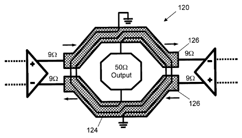
[0031] Reference is made to Figure 4 to describe an electronic component 120
according to
one embodiment of the present invention. The electronic component includes at
least one first
conductor 124 for operating at a first voltage applied thereto and at least
one second conductor
126 for operating at a second voltage applied thereto. The second voltage is
smaller than the
first voltage and at least a portion of the second conductor 126 is located on
at least one side of
the first conductor 124 whereby the second conductor 126 acts as a shield to
inhibit at least one
of magnetic and electric field from passing from the first conductor 124 to a
surrounding
medium.
[0032] The following examples are provided to further illustrate various
embodiments of the
present invention. These examples are intended to be illustrative only and are
not intended to
limit the scope of the present invention.
[0033] Figure 5 is a simplified schematic diagram of a power amplifier
incorporating
embodiments of the present invention. The power amplifier includes 3 common-
base amplifiers
(stages 1 to 3), each pair of common-base amplifiers at a different stage in
the power amplifier.
An interstage transformer is used for impedance matching to interface between
each stage. A
power dividing balun splits the input signal into 2 paths which are then fed
to each of the 2 input
amplifier stages. A power combining balun sums the amplified signals and
couples them to a 50
Ohm load at the output.
6
CA 02521878 2005-09-29
[0034] Figure 6A shows a simplified plan view of the interstage transformer
for interfacing
stages in the power amplifier of Figure 5, according to an embodiment of the
present invention.
The transformer is indicated generally by the numeral 120 and includes a first
coil, referred to
herein as the first conductor 124, and a second coil, referred to herein as
the second conductor
126. As shown, the first conductor 124 is a 2-turn winding and is connected to
the output (i.e.,
collector) side of the amplifying stage immediately prior to the interstage
transformer 120. As a
result of magnetic coupling, a current flows through the wider second
conductor 126. The
second conductor 126 is connected to the input (i.e., emitter) side of the
amplifying stage
immediately following the interstage transformer 120. The voltage in the first
conductor 124 is
much higher than the voltage in the second conductor 126. In the present
exemplary
embodiment, the voltage fluctuation at the collectors is from about 0.5 to
about 3 Volts, resulting
in a differential output voltage swing of about 2.5 Volts. The voltage
fluctuation at the emitters is
about -0.1 to about 0.3 Volts. Thus, the voltage difference at the emitter
side is about 0.4 Volts.
Clearly the voltage applied to the second conductor 126 is much smaller than
the voltage at the
first conductor 124.
[0035] The second conductor 126 is spaced from the substrate 122 (Figure 6B)
and has a
much lower voltage than the first conductor 124. Thus, the second conductor
126 is used to
form a shield by surrounding the first conductor 124, as shown in the
sectional view of Figure
6B, reducing magnetic field leakage and thereby improving magnetic field
coupling between the
first and second conductors 124, 126. In addition, the electric field
emanating from the first
conductor 124 is confined to a region above the underlying silicon substrate
by the second
conductor 126, thereby reducing the strength of the electric field entering
the inter-metal
dielectric (IMD) and silicon substrate 122 underlying the second conductor
126.
[0036] Current crowding due to the skin effect causes the current to flow
mainly along the
edges of the first conductor 124 that are closest to the second conductor 126.
As shown in
Figure 6B, three edges of the first conductor 124 are approximately equally
spaced from the
second conductor 126. Thus, the current crowds along all three edges of the
first conductor 124
that are closest to the second conductor 126.
[0037] Referring again to Figure 5, the power amplifier also includes a power
combining
balun for combining the balanced (or differential) output from two
differential amplifiers into a
single-ended output.
[0038] Figure 7A shows a simplified plan view of the balun for combining the
output from
7
CA 02521878 2005-09-29
two differential amplifiers into a single-ended output in the power amplifier
of Figure 5, according
to another embodiment of the present invention. The present embodiment
includes many
similar features to those of Figure 6A, and the reference numerals used in
Figure 7A are raised
by 100 to denote similar features of the present embodiment. The balun power
combiner is
indicated generally by the numeral 220 and includes a first conductor 224 and
second conductor
226. The second conductor 226 includes two portions that are connected to the
outputs of the
final common base amplifier stages of Figure 5. In the balun power combiner
220, the second
conductor 226 is physically wider than and operates at lower voltage than the
first conductor
224.
[0039] As a result of magnetic field coupling between the first and second
conductors 224,
226, current flows through the relatively narrow first conductor 224, which
provides the output
for the power amplifier of Figure 5. The voltage in the first conductor 224 is
much higher than
the voltage in the second conductor 226. Because it is disposed between the
first conductor
224 and the underlying substrate, the second conductor 226 forms a shield by
surrounding
three sides of each turn of the fast conductor 224, as best shown in Figure
7B. Thus, the
electric field from the first conductor 224 is confined by the second
conductor 226, thereby
inhibiting the electric field from traveling into the silicon-based substrate
222 (underlying inter-
metal dielectric, or IMD, and silicon layers). This also reduces magnetic
field leakage, thereby
improving magnetic field coupling between first and second conductors 224,
226.
[0040] Current crowding caused by the skin effect forces the current to flow
on edges of the
first conductor 224 that are closest to the second conductor 226. As shown in
Figure 7B, the
three edges of each turn of the first conductor 224 are approximately equally
spaced from the
second conductor 226. Thus, the current crowds to all three edges of the first
conductor 224
that are closest to the second conductor 226.
[0041] In the present exemplary embodiment, the second conductor 226 acts as a
shield.
Thus, the second conductor 226 of the present embodiment performs a similar
function to that
performed by the second conductor 126 of the first described exemplary
embodiment, which is
to act as a shield for the other conductor or conductors.
[0042] Figure 8A shows a simplified plan view of a four-way power combiner for
use in VLSI
technology, according to another embodiment of the present invention. The
present
embodiment is similar to the embodiment shown in Figure 7A and accordingly,
like reference
numerals are used to denote like parts. According to the present embodiment,
the low
8
CA 02521878 2005-09-29
impedance (0r2 to 12.5f2) second conductor 226 is used to shield the higher
voltage first
conductor 224 (with impedance Of2 to 502) from the substrate 222 to reduce
electric field
leakage. Referring to Figure 8B, the top layer of metal is about 4Nm thick,
while the second
metal layer (the layer of metal forming the second conductor 226 that is
located between the
first conductor 224 and the substrate 222) is about 1.25pm thick. The spacing
between the
second conductor 226 and the first conductor 224 is about SNm.
[0043] In the present embodiment, a further metal layer 228 is located between
the primary
conductor 226 and the substrate 222. The further metal layer 228 includes a
plurality of spaced
apart, substantially parallel floating metal strips, as disclosed in the
applicants own United States
patent application serial No. 10/425,414, filed April 29, 2003 and published
under United States
patent publication number 20040155728 on August 12, 2004, the entire contents
of which are
incorporated herein by reference. These metal strips are tightly spaced such
that electric field is
further inhibited from passing through to the underlying substrate layer. The
spacing between
the strips is about equal to the minimum dimension (width) of the metal strips
(about 1.ONm).
[0044] Reference is now made to Figures 9A to 9C to describe a self-shielded
inductor
according to another embodiment of the present invention. The shielded
inductor 320 includes
a conductor 330 with a first terminal 332 at an end thereof, to which a time-
varying voltage is
applied. The conductor 330 is connected to a second metal layer in the form of
a conductor 334
that acts to shield electric field from the first conductor 330 to the
surroundings. A time-varying
voltage that is opposite in polarity and much lower in amplitude to that
applied to the first
terminal 332, is applied to an end terminal of the second conductor 334
(referred to herein as
the second terminal 336). The application of a lower amplitude time-varying
voltage that is
opposite in polarity to the second terminal 336 results in a portion of the
conductor 334 being at
or close to zero potential (zero potential for static or time-varying voltage)
on the second
conductor 334, thereby providing the shield.
[0045] Referring now to Figures 10A-10C, a shielded inductor 320 according to
another
embodiment is shown. The shielded inductor 320 is similar to that shown in
Figures 9A to 9C
and includes a further metal layer in the form of another conductor 340. The
conductor 340 is
similar to the conductor 334 and is also attached to the conductor 330 by the
via 338. The
conductors 334, 340 are also connected by a second via 342, proximal the
second terminal 336.
Thus, in the present embodiment, the conductors 334, 340 each include a
portion at or close to
zero potential, thereby providing a pair of shields, one above the conductor
330 and one below
9
CA 02521878 2005-09-29
the conductor 330.
[0046] Referring now to Figures 11A to 11 C a shielded inductor 320 according
to another
embodiment is shown. The present embodiment includes a symmetrical conductor
330
including a pair of differentially driven terminals resulting in a low-voltage
portion 326 where the
time-varying voltage is less than that in the remainder 324 (higher voltage
portion) of the
conductor 330. The shielded inductor 320 also includes a metal layer 334, or
shield, attached to
the symmetrical conductor 330 proximal the low-voltage portions 326. The metal
layer 334 is
connected by the first via 338A and a second via 3388 to the conductor 330 and
includes a
point of zero potential or virtual ground 344. In the present embodiment, the
low voltage
portions 326 are similar to the low-voltage portion of the previously
described shielded
inductors. Thus the metal layer 334 with the virtual ground 344 shields the
symmetrical
conductor 330 in a similar manner to the previously described embodiments.
[004Tj Fig. 12 is a bottom perspective view of a shielded inductor 320
according to still
another embodiment of the present invention. The shielded inductor 320
includes a
symmetrical conductor 330. In this embodiment, the symmetrical conductor 330
is shielded
along an inside turn and along an outside turn in the same plane as the
symmetrical conductor
330. An inner metal turn 346 is coplanar to, spaced from and extends around
the inside of the
symmetrical conductor 330. The inner metal turn 346 is connected as a
continuation of the
symmetrical conductor 330 using crossover via 338 and includes a virtual
ground 344.
[0048] Similarly, an outer metal turn 348 is coplanar to, spaced from and
extends around
the outside of the symmetrical conductor 330. The outer metal turn 348 is
connected to the
inner metal turn 346 by further vias and interconnect layers 350. Thus both
the inner metal turn
346 and the outer metal turn 348 effectively shield the inner side and outer
side, respectively, of
the symmetrical conductor 330.
[0049] Fig. 13 is a bottom perspective view of a shielded inductor 320
according to yet
another embodiment of the present invention. The shielded inductor 320 of the
present
embodiment is similar to the embodiment described with reference to Figure 12
and further
includes a metal layer 334 that acts as a shield between the conductor 320 and
the substrate
(not shown). The metal layer 334 of the present embodiment is made of narrow
metal
conductor rather than a solid plate. The metal shield conductors are attached
to the vias and
interconnect layers 350 and are therefore routed in parallel with the inner
and outer metal turns
346 and 348, respectively. In the present embodiment, the metal shield
conductors 334 include
CA 02521878 2005-09-29
the virtual ground 344. Thus the conductors 334 reduce the electric field
emanating into the
substrate and the current induced in the substrate is reduced.
[0050) While the embodiments described herein are directed to particular
implementations
of the present invention, it will be understood that modifications and
variations to these
embodiments are within the scope and sphere of the present invention. For
example, the size
and shape of many of the features can vary while still performing the same
function. The
present invention is not limited to electronic components fabricated on
silicon-based (silicon plus
inter-metal dielectrics) substrates, as other substrates can be used. Also,
the invention is not
limited to, for example, a four-way power combining balun or the inductors
shown and described
as other baluns and transformer and inductor configurations are possible, such
as eight-way
power combining baluns, or step-up/step-down transformers. Those skilled in
the art may
conceive of still other variations, all of which are believed to be within the
sphere and scope of
the present invention.
11