Note: Descriptions are shown in the official language in which they were submitted.
CA 02521881 2005-10-06
WO 2004/102632 PCT/US2004/014919
HIGH POWER AlInGaN BASED MULTI-CHIP
LIGHT EMITTING DIODE
FIELD OF THE INVENTION
[0001] The present invention relates generally to light emitting diodes
(LEDs), as well as methods for producing and operating the same. More
particularly, the present invention relates to an LED having an improved
design
which provides enhanced output characteristics. Even more particularly, the
present invention relates to a high power AlInGaN LED assembly comprising
multiple highly efficient, elongated chips assembled in an optimized
reflective cup
package.
BACKGROUND OF THE INVENTION
[0002] Light emitting diodes (LEDs) for use as indicators are well know.
LEDs have been used extensively for this purpose in consumer electronics. For
example, red LEDs are commonly used to indicate that power has been applied to
such devices as radios, televisions, video recorders (VCRs) and the like.
[0003] Although such contemporary LEDs have proven generally suitable for
their intended purposes, they possess inherent deficiencies which detract from
their
overall effectiveness and desirability. For example, the power output of such
contemporary LEDs is not as great as is sometimes desired. This limits the
ability
of contemporary LEDs to function in some applications, such as providing
general
illumination, e.g., ambient lighting. Even high power contemporary LEDs do not
provide sufficient illumination for such purposes.
[0004] Contemporary LEDs are also less efficient than desirable, thus
making their use for general illumination less attractive. High power
contemporary
LEDs are even less efficient than standard LEDs, thus making high power LEDs
even less attractive for some applications.
[0005] Attempts to overcome the limitation of contemporary LEDs
associated
with insufficient power output include the use of multiple LEDs which are
ganged so
CA 02521881 2005-10-06
WO 2004/102632 PCT/US2004/014919
as to provide the desired illumination. However, the use of multiple LEDs is
more
expensive than desired and inherently increases the size or volume of the
illumination device, making it unsuitable for some applications.
[0006] AlInGaN based LEDs have attracted much attention in recent years
due to their high potential for use as a solid state light source which is
suitable for
replacing traditional incandescent and fluorescent lighting. Although still
not as
efficient as desired, the efficiency of contemporary LEDs has been improved so
much in the last decade that it is now higher than the efficiency of the
common
tungsten lamp.
[0007] LEDs produce light which is monochromatic. Thus, they are
typically
not suitable for general illumination, for which white light is generally
desirable.
However, by combining a blue AlInGaN LED with yellow phosphors, white light
can
be produced. This approach is now being used extensively in the manufacturing
of
white LEDs.
[0008] Nevertheless, white LEDs are more extensively used in backlight
applications for liquid crystal displays (LCDs) than for general illumination.
This is
more due to the cost of making AlInGaN LEDs than to performance
considerations.
Ultimately one needs to optimize both cost and performance, so that LEDs can
be
competitive with respect to traditional light sources.
[0009] One issue relating to LEDs is that their efficiency can be
adversely
affected by heat generated within the device itself. This limits the amount of
electrical power that can be used to drive an LED, and thus results in a
limitation on
maximum output optical power from an LED since the amount of light that can be
generated is roughly proportional to the input electrical power.
[0010] The fundamental reason for lower efficiency caused by heat is due
to
temperature rises in the LED die. Higher operating temperatures not only
.degrade
the light output efficiency, but also substantially reduce the life of the
LED. Since
heat generation in the LED is unavoidable, scientists have been trying to
reduce the
temperature rise by improving the heat removal rate. This can be accomplished
by
placing a heat sink close to the active region of the device and by choosing
high
thermal conductivity material for the heat sink.
2
CA 02521881 2005-10-06
WO 2004/102632 PCT/US2004/014919
[0011] Another approach is to use larger device size so that both the
contact
area to the outer thermal contact, as well as the total heat capacity,
increases. For
the same amount of heat generated, a larger device will remain cooler than a
smaller device, thereby facilitating operation with higher input power. Of
course, the
higher the input power is, the higher the output optical power will be.
Therefore, for
a larger LED chip the total power that can be delivered from a single device
increases and a cost saving is expected, since one large size device replaces
several small size ones.
[0012] Referring now to Figure 1, a simplified schematic of an AlInGaN on
sapphire LED is shown. The most commonly used device size for an AlInGaN on
sapphire LED is about 300 x 300 microns. The device is normally operated at 20-
30
milliamps and 3.5 volts. Some contemporary designs may have different
geometry,
but the dimensions of the sides are approximately similar, i.e., the aspect
ratio
between the two sides of a contemporary LED is approximately 1. This is mainly
due to the size of the conventional LED package, wherein a cup shaped recess
is
configured for an LED chip to mount therein and has a dimension of
approximately
400 micron in either round or square.
[0013] Referring now to Figure 2, a simplified schematic of a
contemporary
large size (high power) LED chip is shown. Recently, such large size AlInGaN
based LED chips have become readily available. The dimension of these large
size
chips is about 1000 x 1000 microns. Usually, the actual device area (excluding
the
bond pads and etched recess) of a large chip is designed and optimized to
operate
under similar current density with respect to smaller contemporary LEDs, so
that
the heat generation rate per unit area is about the same in both instances. In
general, the large size chip is operated at about 250-350 milliamps and 3.5
volts.
[0014] When designing a large size device, one needs to pay extra
attention
to how current will spread in the device, so that a minimum of current
crowding
occurs. Such current crowding occurs because the lateral resistance increases
with
the chip dimension and because current tends not to travel to far laterally
before
traveling vertically. When this happens, sufficient electrical contact
distribution
needs to be provided so as to ensure that substantially all of the lateral
current is
3
CA 02521881 2005-10-06
WO 2004/102632 PCT/US2004/014919
evenly distributed. In actual practice, an inter-digital finger pattern is
used, such as
the one shown in Figure 2.
[0015] Even though large size devices can deliver more output power per
device, there is a light extraction problem associated with large dimension
devices.
When light is generated in an LED, some light escapes easily from the chip and
some light doesn't, depending on the angle at which the light impinges upon
the
interface between the LED and the outside media. When the optical index of
refraction of the media is smaller than the index of the LED material, light
inside the
LED will be reflected back to the LED when the angle of incidence is greater
than a
critical angle. The reflected light then bounces inside the LED until it finds
a way out
or is absorbed. The light intensity attenuates due to absorption in the bulk
material.
[0016] The more light travels inside the LED and the larger the index of
refraction of the LED material is, the less light will escape. Thus, it is
desirable to
minimize the number of bounces and the total travel distance before light can
escape for any light transmissive layer of an LED.
[0017] Referring now to Figure 3A, as the device size increases, light
has a
tendency to bounce more and thus travel a longer distance before exiting the
device, resulting in increased light loss. Figure 3B shows that light tends to
bounce
fewer times in a smaller device and thus travels a shorter distance. This is
an
especially serious issue for AlInGaN on sapphire LEDs, since both AlInGaN and
sapphire have relatively higher indices of refraction when compared to other
LED
materials such as GaAs and AlInGaP (for infrared and red to amber colors).
Because of the high index of refraction of AlInGaN and sapphire, a large
portion of
light actually travels in these two regions and escapes from the sides.
Therefore,
the lateral dimension of the device is an important consideration for AlInGaN
LEDs.
[0018] One remedy to this problem involves mounting the chip upside down
and providing a mirror coating on the epitaxial side, so as to redirect the
light output
thereof toward the substrate side. Since the index of refraction of sapphire
(n=1.7)
is lower than that of AlInGaN (n=2.5), sapphire provides a good index matching
between the AlInGaN LED and the media (n=1.5 for most epoxy). The mirror
coating on the epitaxial side reflects light toward the substrate. This design
provides
=
4
CA 02521881 2005-10-06
WO 2004/102632 PCT/US2004/014919
a better pathway for light to escape therefrom. In the actual practice, light
efficiency
is twice that of the non-flipped large size LED. However, the cost to make
this
device is high since not only a sub-mount is required between the chip and the
final
package, but also a precise alignment is needed to ensure proper electrical
contact
between the chip contact pads and the sub-mount. So far, there is no evidence
that
such fabrication can be a high yield process.
[0019] In the device shown in Figure 2, there are two issues with respect
to
light extraction. Besides the light which escapes from the device without
bounces,
the remaining light basically travels in the epitaxial layer region and the
substrate
region before finding an exit. Most of the light exits from the sides of the
device.
For light traveling in the substrate region, it suffers the same problems as
discussed
above with reference to Figure 3A. That is, the light attenuates due to bulk
and
interface absorptions. This is true for both directions, i.e., parallel and
perpendicular
to the fingers.
[0020] For light traveling in the epitaxial layers, the light loss due to
the large
dimension is only along the parallel direction to the fingers. Since the
distance light
travels perpendicular to the fingers is much shorter before impinging upon the
two
sides, light escapes relatively easily with much less loss as compared to the
other,
longer, direction.
[0021] However, light which exits from one of the sides could hit the
metal
finger and then be absorbed thereby. Unfortunately, the most commonly used
metals, such as Au or an Au based alloy, readily absorb light in the blue
spectrum.
[0022] In actual practice, as depicted in Figure 1 and Figure 2, the
light
extraction efficiency of the 1000 x 1000 micron device is only 1/3 of that of
the 300
x 300 micron device, due to the issues discussed in detail above. Because of
this,
even though the device area of the 1000 x 1000 micron chip is more than 10
times
of the 300 x 300 micron chip, the output power is only about 3-4 times.
[0023] As such, although the prior art has recognized, to a limited
extent, the
problems of insufficient illumination and poor efficiency, the proposed
solutions
have, to date, been ineffective in providing a satisfactory remedy. Therefore,
it is
desirable to provide an LED having increased optical output power and enhanced
CA 02521881 2012-03-12
54825-1
efficiency. More particularly, it is desirable to provide an LED having a
larger active
surface, so as to provide increased brightness and efficiency with respect to
contemporary LEDs.
BRIEF SUMMARY OF THE INVENTION
According to one aspect of the present invention, there is provided a
method for forming a light emitting diode chip, the method comprising:
providing a
substantially transparent substrate; forming at least one active region upon
the
substrate, the at least one active region comprising an upper LED layer and a
lower
LED layer; forming an upper contact finger upon the upper LED layer; forming a
lower
contact finger upon the lower LED layer; forming a reflector intermediate the
active
region and the lower contact finger, the reflector being configured to reflect
light
directed from the active region toward the lower contact finger away from the
lower
contact finger so as to enhance a brightness of the light emitting diode chip;
and
cutting the substrate to form at least one light emitting diode chip having an
active
area with an aspect ratio which is greater than approximately 1.5 to 1.
According to another aspect of the present invention, there is provided
a light emitting diode chip comprising: a substantially transparent substrate;
an active
region formed upon the substrate and comprising an upper LED layer and a lower
LED layer; an upper contact finger formed upon the upper LED layer; a lower
contact
finger formed upon the lower LED layer; and a reflector disposed intermediate
the
active region and the lower contact finger, the reflector being configured to
reflect
light directed from the active region toward the lower contact finger away
from the
lower contact finger so as to enhance a brightness of the light emitting diode
chip,
and wherein an aspect ratio of the active area is greater than approximately
1.5 to 1.
According to still another aspect of the present invention, there is
provided a light emitting diode chip comprising: a substantially transparent
substrate;
an active region formed upon the substrate; an upper LED layer and a lower LED
layer cooperating to define the active region; an upper contact finger formed
upon the
6
CA 02521881 2012-03-12
' 54825-1
upper LED layer; a lower contact finger formed upon the lower LED layer; an
upper
bond pad in electrical contact with the upper contact finger; a lower bond pad
in
electrical contact with the lower contact finger, wherein the upper bond pad
and the
lower bond pad are formed at diagonally opposite corners of the substantially
transparent substrate; and a reflector disposed intermediate the active region
and the
lower contact finger, the reflector being configured to reflect light directed
from the
active region toward the lower contact finger away from the lower contact
finger so as
to enhance a brightness of the light emitting diode chip.
According to yet another aspect of the present invention, there is
provided a light emitting diode lamp comprising: a package comprising a
plurality of
recesses arranged around a periphery of the package; a plurality of light
emitting
diode chips each chip disposed within a respective different recess of the
plurality of
recesses each of the light emitting diode chips comprising: a substantially
transparent
substrate; a single active region formed upon the substrate from an upper LED
layer
and a lower LED layer; an upper contact finger formed upon the upper LED
layer; a
lower contact finger formed upon the lower LED layer; and a reflector disposed
intermediate the active region and the lower contact finger, the reflector
being
configured to reflect light directed from the active region toward the lower
contact
finger away from the lower contact finger so as to enhance a brightness of the
light
emitting diode chip, and wherein an aspect ratio of the active area is greater
than
approximately 1.5 to 1.
According to a further aspect of the present invention, there is provided
an illumination device comprising: a power source; a light emitting diode lamp
in
electrical communication with the power source, the light emitting diode lamp
comprising: a package comprising a plurality of recesses arranged around a
periphery of the package; a plurality of light emitting diode chips each chip
disposed
within a respective different recess of the plurality of recesses each of the
light
emitting diode chips comprising: a substantially transparent substrate; a
single active
region formed upon the substrate from an upper LED layer and a lower LED
layer; an
upper contact finger formed upon the upper LED layer; a lower contact finger
formed
6a
CA 02521881 2012-03-12
54825-1
upon the lower LED layer; and a reflector disposed intermediate the active
region and
the lower contact finger, the reflector being configured to reflect light
directed from the
active region toward the lower contact finger away from the lower contact
finger so as
to enhance a brightness of the light emitting diode chip, and wherein an
aspect ratio
of the active area is greater than approximately 1.5 to 1.
[0025] An embodiment of the present invention comprises a light
emitting
diode chip having a substantially transparent substrate and having an aspect
ratio
which defines an elongated geometry, so as to provide enhanced efficiency and
brightness, and a method for forming the same.
[0026] These, as well as other advantages of the present invention, will be
more apparent from the following description and drawings. It is understood
that
changes in the specific structure shown and described may be made within the
scope
of the claims, without departing from the spirit of the invention.
[0027] The invention can be better visualized by turning now to the
following
drawings wherein like elements are referenced by like numerals.
BRIEF DESCRIPTION OF THE DRAWINGS
[0028] The invention and its various embodiments can now be better
understood by turning to the following detailed description of the preferred
embodiments which are presented as illustrated examples of the invention
defined
6b
CA 02521881 2005-10-06
WO 2004/102632 PCT/US2004/014919
in the claims. It is expressly understood that the invention as defined by the
claims
may be broader than the illustrated embodiments described below.
[0029] Figure 1 is a semi-schematic representation of a typical
contemporary
standard (300 x 300 micron) AlInGaN LED formed upon a transparent sapphire
substrate;
[0030] Figure 2 is a semi-schematic representation of a contemporary high
power (1,000 x 1,000 micron) AlInGaN LED, showing the interdigital contact
fingers
thereof;
[0031] Figure 3A is a side view showing light propagating along a long
path
within a higher index of refraction material (such as a sapphire substrate or
an
epitaxial LED layer) until it finally escapes into a lower index of refraction
material
(such as air);
[0032] Figure 3B is a side view showing light propagating along a short
path
within a higher index of refraction material (such as a sapphire substrate or
an
epitaxial LED layer) until it finally escapes into a lower index of refraction
material
(such as air);
[0033] Figure 4 is a is a perspective view of an elongated power LED
having
a high aspect ratio and having a reflective coating formed upon one sidewall
thereof
according to the present invention;
[0034] Figure 5A is a plan view showing one exemplary arrangement of four
250 x 1000 micron LEDs disposed within a recessed package having a reflective
coating formed upon the inside surface of the package;
[0035] Figure 5B is a cross-sectional side view of the exemplary
arrangement of four 250 x 1000 micron LEDs disposed within a recessed package
of Figure 5A, taken along line 5B thereof;
[0036] Figure 6A is a plan view showing another exemplary arrangement of
four 250 x 1000 micron LEDs disposed within a recessed package having a
reflective coating formed upon the inside surface of the package;
7
CA 02521881 2005-10-06
WO 2004/102632 PCT/US2004/014919
[0037] Figure 6B is a cross-sectional side view of the exemplary
arrangement of four 250 x '1000 micron LEDs disposed within a recessed package
of Figure 6A, taken along line 6B thereof;
[0038] Figure 7 is a semi-schematic cross-sectional view of a flashlight
formed according to the present invention;
[0039] Figure 8A is the exemplary arrangement of four LEDs disposed
within
a recessed package of Figure 5A, showing the LEDs electrically connected to
one
another in series;
[0040] Figure 8B is the exemplary arrangement of four LEDs disposed
within
a recessed package of Figure 5A, showing two pairs of the LEDs electrically
connected to one another in parallel; and
[0041] Figure 8C is the exemplary arrangement of four LEDs disposed
within
a recessed package of Figure 6A, showing all four of the LEDs electrically
connected to one another in parallel.
DETAILED DESCRIPTION OF THE PREFERRED EMBODIMENTS
[0042] Many alterations and modifications may be made by those having
ordinary skill in the art without departing from the spirit and scope of the
invention.
Therefore, it must be understood that the illustrated embodiment has been set
forth
only for the purposes of example and that it should not be taken as limiting
the
invention as defined by the following claims. For example, notwithstanding the
fact
that the elements of a claim are set forth below in a certain combination, it
must be
expressly understood that the invention includes other combinations of fewer,
more
or different elements, which are disclosed in above even when not initially
claimed
in such combinations.
[0043] The words used in this specification to describe the invention and
its
various embodiments are to be understood not only in the sense of their
commonly
defined meanings, but to include by special definition in this specification
structure,
material or acts beyond the scope of the commonly defined meanings. Thus if an
element can be understood in the context of this specification as including
more
8
CA 02521881 2005-10-06
WO 2004/102632 PCT/US2004/014919
than One meaning, then its use in a claim must be understood as being generic
to
all possible meanings supported by the specification and by the word itself.
[0044] The definitions of the words or elements of the following claims
are,
therefore, defined in this specification to include not only the combination
of
elements which are literally set forth, but all equivalent structure, material
or acts for
performing substantially the same function in substantially the same way to
obtain
substantially the same result. In this sense it is therefore contemplated that
an
equivalent substitution of two or more elements may be made for any one of the
elements in the claims below or that a single element may be substituted for
two or
more elements in a claim. Although elements may be described above as acting
in
certain combinations and even initially claimed as such, it is to be expressly
understood that one or more elements from a claimed combination can in some
cases be excised from the combination and that the claimed combination may be
directed to a subcombination or variation of a subcombination.
[0045] Insubstantial changes from the claimed subject matter as viewed by
a
person with ordinary skill in the art, now known or later devised, are
expressly
contemplated as being equivalently within the scope of the claims. Therefore,
obvious substitutions now or later known to one with ordinary skill in the art
are
defined to be within the scope of the defined elements.
[0046] The claims are thus to be understood to include what is
specifically
illustrated and described above, what is conceptionally equivalent, what can
be
obviously substituted and also what essentially incorporates the essential
idea of
the invention.
[0047] Thus, the detailed description set forth below in connection with
the
appended drawings is intended as a description of the presently preferred
embodiments of the invention and is not intended to represent the only forms
in
which the present invention may be constructed or utilized. The description
sets
forth the functions and the sequence of steps for constructing and operating
the
invention in connection with the illustrated embodiments. It is to be
understood,
however, that the same or equivalent functions may be accomplished by
different
9
CA 02521881 2012-03-12
54825-1
embodiments that are also intended to be encompassed within the scope of the
invention.
[0048] According to one aspect, the present invention comprises a method
for fabricating a light emitting diode (LED) chip, the method comprises
forming a
substantially transparent substrate having an aspect ratio which defines an
elongated geometry. More particularly, the present invention comprises a
method
for forming a high power light emitting diode chip, wherein the method
comprising
providing a substantially transparent substrate, forming at least one active
region
upon the substrate, and cutting, e.g., dicing, the substrate to form at least
one light
emitting diode chip having an active area with an aspect ratio which is
greater than
approximately 1.5 to 1.
[0049] Preferably, the aspect ratio of the active area is greater than
approximately 2 to 1. Preferably, the aspect ratio of the active area is
between
approximately 1.5 to 1 and approximately 10 to 1. Preferably, the aspect ratio
of
the active area is approximately 4 to 1. Preferably, the width thereof is
approximately 250 microns and the length thereof is approximately 1000
microns.
[0050] However, those skilled in the art will appreciate that various
equivalent elongate structures of the active area likewise suitable. For
example,
the active area may alternatively be defined by a plurality of elongate
structures
which are integrally formed with respect to one another so as to define a more
complex configuration. One example of such a complex configuration formed from
elongate structures is a cross. Another example is a plurality of spokes
radiating
from a common central point, much like the spokes of a wagon wheel, thus
generally providing the appearance of an asterisk.
[0051] Preferably, the active region is configured to operate at between
approximately 3.0 volts and approximately 3.5 volts and between approximately
60
milliamps and approximately 90 milliamps. However, those skilled in the art
will
appreciate that various other operating parameters are likewise suitable,
particularly when the active area is defined by materials other than AlInGaN.
[0052] The active regions are optionally in electrical communication with
one
another so as to define a network such that voltage within the network tends
to be
CA 02521881 2005-10-06
WO 2004/102632 PCT/US2004/014919
maximized without current through any light emitting diode chip being greater
than
a predetermined value. By maximizing voltage within the network, the
efficiency of
power transmission therein is desirably enhanced.
[0053] Preferably, one light emitting diode device is formed upon each
substrate and the active area substantially covers substantially the entire
surface of
each substrate. However, a plurality of elongated active areas may
alternatively be
formed upon a common substrate. In this instance, the active areas will not
completely cover the substrate.
[0054] For example, an array of elongated active areas may be etched onto
a single substrate. As a further example, a cross or radiating spoke patterned
active area may be formed upon a substrate. In these two examples, the active
area will not cover substantially the entire surface of the substrate. For
instance, it
will not cover the area between the radiating spokes.
[0055] Preferably, the substrate comprises a material selected from the
group comprising sapphire, spinel, glass, ZnO, SIC, MgO, GaN, AIN, and AlGaN.
Preferably, the active region comprises AlInGaN. However, as those skilled in
the
art will appreciate, other materials for the substrate and/or the active area
are
likewise suitable.
[0056] According to one aspect, the method of the present invention
comprises forming an upper LED layer and a lower LED layer (with opposite type
with respect to the upper LED layer) which cooperate to define the active
region;
forming an upper contact finger upon the upper LED layer; forming a lower
contact
finger upon the lower LED layer; and forming a reflector intermediate the
active
region and the lower contact finger, the reflector being configured to reflect
light
directed from the active region toward the lower contact finger away from the
lower
contact finger so as to enhance a brightness of the light emitting diode chip.
Preferably, the reflector is formed upon the active region intermediate the
active
region and the lower contact finger.
[0057] The reflector may comprise either a dielectric reflector or a
metal
reflector. If the reflector comprises a metal reflector, then a transparent
insulator is
11
CA 02521881 2005-10-06
WO 2004/102632 PCT/US2004/014919
preferably formed upon the active region intermediate the active region and
the
lower contact finger to electrically insulate the reflector from the active
region.
[0058]
According to one aspect, the present invention comprises a light
emitting diode chip comprising a substantially transparent substrate and
having an
aspect ratio which defines an elongated geometry. More particularly, the
present
invention comprises a high power light emitting diode chip comprising a
substantially transparent substrate, an active region formed upon the
substrate, and
wherein an aspect ratio of the active area is greater than approximately 1.5
to 1.
[0059] ,
According to one aspect, the present invention comprises high power
light emitting diode chip comprising a reflector disposed intermediate the
active
region and the lower contact finger, the reflector being configured to reflect
light
directed from the active region toward the lower contact finger away from the
lower
contact finger so as to enhance a brightness of the light emitting diode chip.
[0060]
According to one aspect, the present invention comprises a high
power light emitting diode lamp comprising a package and at least one light
emitting diode chip disposed within the package.
[0061] The
package preferably comprises four reflective sides and a
reflective bottom. The package preferably defines a rectangle. The package
preferably defines a square. However, as those skilled in the art will
appreciate, the
package may alternative define any other desired shape. For example, the
package may alternative be round.
[0062] The
high power light emitting diode lamp preferably comprises a
plurality of light emitting diode chips. The light emitting diode chips may be
electrically in series with one another, electrically in parallel with one
another, or
electrically in some combination of series and parallel with one another. For
example, in a high power light emitting diode lamp having four light emitting
diodes,
pairs of the light emitting diodes may individually be in parallel with one
another and
the two pairs then (each as a grouped pair) be in series with one another.
[0063]
Preferably, the package is configured such that a manufacturer who is
incorporating the high power light emitting diode lamps of the present
invention into
12
CA 02521881 2005-10-06
WO 2004/102632 PCT/US2004/014919
an illuminator product can easily select the desired electrical configuration
(series,
parallel, or a combination of series and parallel) of the light emitting
diodes. For
example, such selection may be performed by bonding conductors to selected
pads
of the high power light emitting diode lamp, by selecting the position of
switches, by
adding or moving jumpers, by burning or removing jumpers, or by any other
desired
method.
[0064] The high power light emitting diode lamp preferably comprises four
light emitting diode chips. The four light emitting diode chips are preferably
configured to generally define a square.
[0065] Optionally, the light emitting diode chips may be configured to
generally define a linear array thereof. Alternatively, the light emitting
diodes may
be disposed end-to-end so as to define the outline of a square. ,
[0066] The package preferably comprises at least one recess with a
reflective coating therein, the light emitting diode(s) being disposed within
the
recess. The package optionally comprises a plurality of recesses, each recess
having a reflective coating therein, at least one light emitting diode, being
disposed
within each recess. For example, the package may comprise a recessed package
having four recesses, each recess having a reflective coating therein, one
light
emitting diode being disposed within each of the four recesses.
[0067] According to one aspect of the present invention, the package
comprises a recessed package having four elongated recesses, each elongated
recess having a reflective coating formed therein, and one light emitting
diode is
disposed within each elongated recess.
[0068] According to one aspect of the present invention, an illumination
device comprise a power source and at least one high power light emitting
diode
lamp in electrical communication with the power source. The power source may
comprise, for example, at least one battery, a plug configured to be connected
to a
wall socket, or an AC power source and a DC power supply coupled to convert AC
current from the AC power source into DC power suitable for operating the
light
emitting diodes.
13
CA 02521881 2005-10-06
WO 2004/102632 PCT/US2004/014919
[0069] Thus,
the present invention provides an LED chip design which
alleviates problems (such as poor efficiency and inadequate brightness)
associated
with contemporary LED chips. The chip has a high aspect ratio between the two
adjacent sides thereof, so that light can easily escape from the long
dimension side,
thus substantially enhancing the brightness of the device. The
elongated
configuration of the LED chip also enhances heat dissipation, thus allowing
the
device to be operated at higher current levels to facility further enhancement
of the
light output thereof, as well as for improvement of the efficiency thereof.
[0070] The
present invention is illustrated in Figures 1-6B, which depict
presently preferred embodiments thereof.
[0071]
Referring now to Figure 1, a contemporary standard 300 x 300 micron
AlInGaN LED formed upon a transparent sapphire substrate is shown. This
contemporary device comprises a transparent sapphire substrate 11, AlInGaN
epitaxial layers 12 formed upon the substrate 11, a active region 13 defined
by the
AlInGaN epitaxial layers 12, an upper or P bond pad 14 formed upon upper ones
epitaxial layers 12, a lower or N bond pad 15 formed upon lower ones of the
epitaxial layers 12 and a P current spreading layer 16.
[0072]
Referring now to Figure 2, a contemporary high power 1000 x 1000
micron AlInGaN LED formed upon a transparent sapphire substrate is shown. This
high power LED is an attempt to provide a brighter LED than the standard LED
shown in Figure 1. Because of its larger size, interdigit contact fingers 26,
27 are
used to spread current through the active layer. This larger contemporary
device
comprises a transparent sapphire substrate 21, AlInGaN epitaxial layers 22
formed
upon the substrate 21, a active region 23 defined by the AlInGaN epitaxial
layers
22, an upper or P finger interconnect 24 formed upon upper ones of the
epitaxial
layers 22 and a lower or N finger interconnect 25 formed upon lower ones of
the
epitaxial layers 22. Upper or P contact fingers 26 spread from the P finger
interconnect 24 and lower or N contact fingers 27 similarly spread from the N
finger
interconnect 25.
[0073] Referring now to Figures 1 and 2, when the size of contemporary
chips size increases from 300 x 300 microns (Figure 1) to 1000 x 1000 microns
14
CA 02521881 2005-10-06
WO 2004/102632 PCT/US2004/014919
(Figure 2), the optical output efficiency decreases by about 60% - 70%. Thus,
although the high power LED does provide increased brightness, it does so by
sacrificing efficiency.
[0074] Referring now to Figures 3A and 3B, this reduction in optical
output
efficiency as the size of the chip increases is due to the increase path
length that
light must travel, on average, before exiting the device. Light traveling in
any layer
of the LED, such as the active layer or the substrate, must typically be
reflected
several times prior to exiting the device. Of course, the larger the LED is,
the
longer the path is and the more opportunities that exist for absorption of the
light
both within the layer and at the interface between adjacent layers. Thus,
light
traveling along a longer path (such as through a larger chip), as shown is
Figure
3A, will be attenuated more, on average, than light traveling along a shorter
path
(such as through a smaller chip), as shown in Figure 3B.
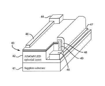
[0075] Referring now to Figure 4, an LED having an elongated geometry
according to the present invention is shown. The present invention comprises a
transparent sapphire substrate 41, AlInGaN epitaxial layers 42 formed upon the
substrate 41, a active region 43 defined by the AlInGaN epitaxial layers 42,
an
upper or P bond pad 44 formed upon upper ones of the epitaxial layers 42, a
lower
or N bond pad 15 formed upon lower ones of the epitaxial layers 42, a P
contact
finger 46 extending from the P bond pad 44, and a N contact finger 47
extending
from the N bond pad 45.
[0076] Optionally, a reflective coating 48 is formed upon the epitaxial
layers
42 (and is thus formed upon the active region 43). Alternatively, the
reflective
coating may be formed upon the N contact finger 47 or may otherwise be formed
intermediate the epitaxial layers 42 and the N contact finger 47. The
reflector is
configured so as to reflect light from the epitaxial layers 43 back into the
epitaxial
layers 43 and thus away from the N contact finger 47. In this manner, the
reflected
light may exit the epitaxial layers 43 at some other location (rather than
proximate
he N contact finger 47) and thus contribute to the brightness of the LED
(rather than
be absorbed by the N contact finger 47).
CA 02521881 2005-10-06
WO 2004/102632 PCT/US2004/014919
[0077] The reflector 48 may be either a dielectric reflector or a metal
reflector. If a metal reflector is utilized, then an insulator 49 is formed
upon the
epitaxial layers 42 intermediate the reflector 48 and the epitaxial layers 42
to
prevent undesirable current flow through the reflector 48.
[0078] According to the present invention the loss of light can be
reduced
appreciably by decreasing the size of the chip, and thus the size of the
active area
and the size of the substrate, in one dimension (thus defining an elongated
geometry). By providing a reflective coating or reflector on one side of the
mesa to
avoid undesirable absorption of light by the N contact finger 47, a further,
reduction
of light loss can be provided.
[0079] Since total area of the device is now also reduced with respect to
contemporary high power LEDs, multiple LEDs can be used to increase the power
capacity. A 250 x 1000 micron device is shown in Figure 4 as one exemplary
embodiment of the present invention. Those skilled in the art will appreciate
that
other dimensions and configurations of the present invention are likewise
suitable.
[0080] To maintain the same current density during operation of the
present
invention as in contemporary devices, the present invention is preferably
configured
to operate at 3.0-3.5 volts and 60-90 milliamps (since the active area of the
present
invention is approximately 25% of the active area of a contemporary 1000 x
1000
micron device). In order to produce as much optical output power as the
contemporary 1000 x 1000 micron device, a set of four 250 x 1000 micron
devices
can be assembled in one package.
[0081] Referring now to Figures 5A - 6B, two packaging configurations of
the
present invention are shown. In many applications, a point light source is
preferred
since it generates a spherical light pattern which is useful to construct any
shape of
plane by arranging the point sources in arrays. In order to provide such a
point
source, several elongated chips can optionally be arranged in a single package
so
as to produce a spherical light pattern.
[0082] Both of the packaging examples of Figures 5A and 6A use four 250 x
1000 micron chips. Each chip is arranged in a reflective cup designed to
direct the
side light upward individually.
16
CA 02521881 2005-10-06
WO 2004/102632 PCT/US2004/014919
[0083] The package shown in Figures 5A and 5B is a single recess cup 51
having an upwardly extending centerpiece 52 in the fashion of a tube pan or
bundt
pan. The recess 56 is suitable for receiving a plurality, e.g., four,
individual LED
chips 57a-57d. The interior sides 53 and bottom 54 of the package, including
the
centerpiece 52 are reflective, so as to enhance the amount of light provided
by the
LED.
[0084] The package show in Figures 6A and 6B is a multiple recess cup 61
having a plurality of separate recesses formed therein. Each recess is
configured
to receive a separate LED chip 67a-67d. The interior of each recess 66a-66d,
including the sides 63 and the bottoms 64, is reflective.
[0085] The individual reflective recess 66a-66d for each chip 67a-67d is
advantageous, since without it the side light from the chips could re-enter
the near
by chips from its side.
[0086] Referring now to Figure 7, a semi-schematic cross-sectional view of
a
flashlight shows a high power LED package 72 formed according to the present
invention which is disposed behind a focusing optical coating or reflector 71.
An
electrical connection 73 to batteries 75, in cooperation with spring
electrical contact
76, conductor 77, and switch 74, facilitate operation of the flashlight
according to
contemporary practice. According to this exemplary embodiment of the
flashlight,
the LEDs are powered by three batteries at 4.5 volts. However, those skilled
in the
art will appreciate that various other configurations of the flashlight are
likewise
suitable. Indeed, the present invention may find application in various
different
portable (battery operated) lighting applications.
[0087] An added advantage of the arrangements shown in Figure 5A-6B is
that the operating voltage and current of the total package can be changed
easily
by bonding the chips in series, parallel or a combination of both, as
discussed
above. For example, if all 4 devices are connected in series, then the
operating
parameters will be 12-14 volts and 60-90 milliamps. If they are connected in
parallel, then the operating condition will become 3-3.5 volts and 240-360
milliamps. If 2 devices are in parallel and 2 devices are in series, the
operating
parameters will be 6-7 volts and 120-180 milliamps. This flexibility is useful
for
17
CA 02521881 2005-10-06
WO 2004/102632 PCT/US2004/014919
circuit designer since there are different requirement in power system
applications.
Usually to mitigate electrical power loss in the power distribution network or
local
power supply, high voltage and low current is more desirable than low voltage
and
high current. Examples of different electrical connections of the LEDs are
provided
in Figures 8A, 8B and 8C, discussed below.
[0088] Referring now to Figure 8A, the LEDs of Figure 5A are electrically
connected to one another in series. This configuration of the LEDs operates at
high
voltage and low current. For example, LEDs of the present invention operated
in
this configuration may operate at 14 volts and 90 milliamps.
[0089] Referring now to Figure 8B, two pairs the LEDs of Figure 5A are
electrically connected to one another in pariallel to provide a 2x2
configuration. For
example, LEDs of the present invention operated in this configuration may
operate
at 7 volts and 180 milliamps.
[0090] Referring now to Figure 8C, the LEDs of Figure 5A are all
electrically
connected to one another in parallel. For example, LEDs of the present
invention
operated in this configuration may operate at 3.5 volts and 360 milliamps.
[0091] The advantages of the present invention include superior light
output
efficiency due to both the elongated geometry thereof and the reflective
coating on
the side of the elongated chip. The present invention provides a power LED
device
assembly and package that generates an approximately spherical light pattern
with
superior light output efficiency as compared to contemporary LEDs. Further,
the
present invention provides flexibility in operating voltage and current in the
packaged power LED to facilitate a circuit designer's ability to optimize his
design to
the requirement of the applications.
[0092] It is understood that the various aspects of the exemplary high
power
AlInGaN based multi-chip light emitting diode described herein and shown in
the
drawings represent only presently preferred embodiments of the invention.
Indeed,
various modifications and additions may be made to such embodiments without
departing from the spirit and scope of the invention. For example, the various
different shapes and configuration of the active area, either upon a common or
upon separate substrates, are contemplated. Those skilled in the art will
appreciate
18
CA 02521881 2005-10-06
WO 2004/102632 PCT/US2004/014919
that equivalent structures, shapes and configurations may be formed by
providing a
wide variety of elongated structures and/or portion of structures. Thus, it is
not
necessary that the entire active area define an elongated geometry, but rather
that
some portion or portions of the active are define one or more elongated
geometries.
[0093] Thus, these and other modifications and additions may be obvious
to
those skilled in the art and may be implemented to adapt the present invention
for
use in a variety of different applications.
19