Note: Descriptions are shown in the official language in which they were submitted.
CA 02522270 2005-10-07
WO 2004/093249 PCT/US2004/011147
RFID D'EV'ICES HAVING SELF-COMPENSATING
ANTENNAS AND CONDUCTIVE SHIELDS
BACKGROUND OF THE INVENTION
1. Field of the Invention
[0001] This invenfiion relates to the field of Radio Frequency Identification
(RFID) tags and labels.
. Description of the Related Art
[000] There is no simple definition of what constitutes an antenna, as all
dielectric and conductive objects interact with electromagnetic fields (radio
waves). What are generally called antennas are simply shapes and sizes that
generate a voltage at convenient impedance for connection to circuits and
devices. Almost anything can act to some degree as an antenna. However,
there are some practical constraints on what designs can be used with RFID
tags
and labels.
[0003] First, reciprocity is a major consideration in making a design choice.
This
means that an antenna which will act as a transmitter, converting a voltage on
its
terminals) into a radiated electromagnetic wave, will also act as a receiver,
where
an incoming electromagnetic wave will cause l induce a voltage across the
terminals. Frequently it is easier to describe the transmitting case, but, in
general,
a good transmit antenna will also work well as a receive antenna (like all
rules,
there are exceptions at lower frequencies, but for UHF, in the 900MHz band and
above where RFID tags and labels commonly operate, this holds generally true).
[0004] Nevertheless, even given the above, it is difficult to determine what
is a
'good' antenna other than to require that it is one that does what you want,
where
you want and is built how you want it to be.
[0005] However, there are some features that are useful as guides in
determining whether or not an antenna is 'good' for a particular purpose. When
one makes a connection to an antenna, one can measure the impedance of the
antenna at a given frequency. Impedance is generally expressed as a composite
of two parts; a resistance, R, expressed in ohms, and a reactance, X, also
expressed in ohms, but with a 'j' factor in front fio express the fact that
reactance
1
CA 02522270 2005-10-07
WO 2004/093249 PCT/US2004/011147
is a v~c:'tar ~qo~ntit~n. 'The w~a1'ue of jX can be either capacitive, where
it is a
negative number, or inductive, where it is a positive number.
[0006] Having established what occurs when one measures the impedance of
an antenna, one can consider the effect of the two parts on the antenna's
suitability or performance in a particular situation.
[000] Resistance R is actually a composite of two things; the loss resistance
of
the antenna, representing the tendency of any signal applied to it to be
converted
to heat, and the radiation resistance, representing energy being 'lost' out of
fihe
antenna by being radiated away, which is what is desired in an antenna. The
rafiio of the loss resistance and the radiation resistance is described as the
antenna efficiency. A low efficiency antenna, with a large loss resistance and
relatively small radiation resistance, will not work well in most situations,
as the
majority of any power put into it will simply appear as heat and not as useful
electromagnetic waves.
[0008] The effects of Reactance X are slightly more complex than that~for
Resistance R. Reactance X, the inductive or capacitive reactance of an
antenna,
does not dissipate energy. In fact, it can be lessened, by introducing a
resonant
circuit into the system. Simply, for a given value of +jX (an inductor), there
is a
value of jX (a capacitor) that will resonate / cancel it, leaving just the
resistance
R.
[0009] Another consideration is bandwidth, frequently described using the term
Q (originally Quality Factor). To understand the effect of bandwidth, it is
not
necessary to understand the mathematics; simply, if an antenna has a value of
+jX or jX representing a large inductance or capacitance, when one resonates
this out it will only become a pure resistance over a very narrow frequency
band.
For example, for a system operating over the band 902MHz to 928MHz, if a
highly reactive antenna were employed, it might only produce the wanted R over
a few megahertz. In addition, high Q l narrow band matching solutions are
unstable, in that very small variations in component values or designs will
cause
large changes in performance. So high C~ narrowband solutions are something,
in practical RFID tag designs, to be avoided.
[0010] An RFID tag, in general, consists of 1 ) an RFID chip, containing
rectifiers
to generate a DC power supply from the incoming RF signal, logic fio carry out
fihe
identification function and an impedance modulator, which changes the input
2
CA 02522270 2005-10-07
WO 2004/093249 PCT/US2004/011147
impedance t~ cause a mwd~lated signal to be reflected; and, 2) an antenna as
described above.
[0011] Each of these elements has an associated impedance. If the chip
impedance (which tends to be capacitive) and the antenna impedance (which is
whatever it is designed t~ be) are the conjugate of each other, then one can
simply connect the chip across the antenna and a useful tag is created. For
common RFID chips the capacitance is such that a reasonably I~w Q adequate
bandwidth match can be achieved at IJHF frequencies.
[001] However, sometimes it is not so simple to meet operational demands for
the flag due to environmental or manufacturing constraints, and then other
ways
of achieving a good mafich must be considered. The most common method of
maintaining a desired impedance match, is to place between the antenna and
chip an impedance matching network. An impedance matching network is usually
a network of inductors and capacitors that act to transform both real and
reactive
parts of the input impedance to a desired level. These components do not
normally include resistors, as these dissipate energy, which will generally
lead to
lower performance.
[0013] Difficulties can arise in impedance matching, because the impedance
characteristics of an antenna may be affected by its surroundings. This may in
turn affect the quality of the impedance matching between the antenna and the
RFID chip, and thus the read range for the RFID tag.
[0014] The surroundings that may affect the characteristics of the antenna
include the substrate material upon which the antenna is mounted, and the
characteristics of other objects in the vicinity of the RFID tag. For example,
the
thickness and/or dielectric constant of the substrate material may affect
antenna
operation. As another example, placement of conducting or non-conducting
objects near the tag may affect the operating characteristics of the antenna,
and
thus the read range of the tag.
[0015] An antenna may be tuned fio have desired characteristics for any given
configuration of substrate and objects placed around. For example, if each tag
could be tuned individually to adjust the arm length and/or add a matching
network, consisting of adjustable capacitors and inductors, the tag could be
made
to work regardless of the dielectric constant of the block. However,
individual
tuning of antennas would not be practical from a business perspective.
3
CA 02522270 2005-10-07
WO 2004/093249 PCT/US2004/011147
[0-0~1~~~ As dfscuss.ed above, frequently designers optimize tag performance
for
'free space', a datum generally given a nominal relative dielectric constant
of 1.
However, in the real world, the objects the labels are attached to frequently
do not
have a dielectric constant of 1, but instead have dielectric constants or
environments of nearby objects that vary widely. For example, a label having a
dipole antenna designed and opfiimized for 'free space' that is instead
attached to
an object having a dielectric constant that differs from that of 'free space,'
will
suffer a degraded performance, usually manifesting itself as reduced
operational
range and other inefficiencies as discussed above.
[OO~i~] Therefore, while products having differing fixed dielectric constant
substrates can be accommodated by changing the antenna design from the 'free
space' design to incorporate the new dielectric constant or to compensate for
other objects expected to be nearby the tag, this design change forces the tag
manufacturer to produce a broader range of labels or tags, potentially a
different
type for each target product for which the tag may be applied, hence
increasing
costs and forcing an inventory stocking problem for the tag manufacturers.
[0018] When the tags are to be used on different types of materials that have
a
range of variable dielectric constants, the best design performance that can
be
achieved by the tag or label designer is to design or tune the tag for the
average
value of the range of dielectric constants and expected conditions, and accept
degraded performance and possible failures caused by significant detuning in
specific cases.
[0019] It will be appreciated that improvements would be desirable with regard
to the above state of affairs.
SUMMARY OF THE INVENTION
[0020] According to one aspect of the present invention, an RFID device
includes an antenna structure that includes compensating elements that
compensate, at least to some degree, for changes of the operating
characteristics
of the antenna structure as the structure is placed on or in proximity to a
dielectric
material.
[0021] According to another aspect of the invention, an RFID device includes
an
antenna strucfiure and a conductive plane or layer on opposite sides (faces)
of a
dielectric material.
4
CA 02522270 2005-10-07
WO 2004/093249 PCT/US2004/011147
;~0n22] According to yet artotner aspect of the invention, an RFID device
includes: a dielectric layer; an antenna structure atop a first face of the
dielectric
layer; an RFID chip coupled to the antenna; and a conductive plane atop a
second face of the dielectric layer, wherein the dielectric layer is
interposed
between the conductive plane and the antenna structure. The antenna structure
includes one or more compensating elements that compensate at least in parfi
for
effects of the dielectric layer on operating characteristics of the antenna
structure.
[0023] According to still another aspect of the invention, a method of
configuring
an RFID device includes the steps of: placing an antenna structure of the RFID
device and a conducting plane of the RFID device opposed to one another on
opposite sides of a dielectric layer; and re-tuning the antenna structure to
compensate at least in part for effects of the dielectric layer on performance
of the
antenna structure.
[0024] To the accomplishment of the foregoing and related ends, the invention
comprises the features hereinafter fully described and particularly pointed
out in
the claims. The following description and the annexed drawings set forth in
detail
certain illustrative embodiments of the invention. These embodiments are
indicative, however, of but a few of the various ways in which the principles
of the
invention may be employed. Other objects, advantages and novel features of the
invention will become apparent from the following detailed description of the
invention when considered in conjunction with the drawings.
BRIEF DESCRIPTION OF THE DRAWINGS
[0025] In the annexed drawings, which may not necessarily be to scale:
[0026] Fig. 1 is an oblique view of a radio frequency identification (RFID)
device
in accordance with the present invention;
[0027] Fig. 2 is a plan view of capacitor shown mounted on a dielectric
material;
[0028] Fig. 3 is a plan view of one type of adaptive element in accordance
with
the present invention, an inter-digital capacitor;
[0029] Fig. 4 is a cross-sectional view taken along the line 3-3 of Fig. 3 in
the
direction shown;
[0030] Fig. 5 is a cross-sectional view similar to that of Fig. 4 where the
capacitor is mounted on a thicker material than that of the capacifior in Fig.
4.;
CA 02522270 2005-10-07
WO 2004/093249 PCT/US2004/011147
~00~1'] Fig. 6 ~~s~ a pmn wiwuv~ or another type of adaptive element in
accordance
with the present invention, a meander inductor;
[0032] Fig. 7 is a plan view of an RFID tag structure embodying the present
invention and using meander inductors;
[0033] Fig. 8 is a plan view of an RFID tag structure embodying the present
invention similar to that shown in Fig. 7, where the tag is mounted on a
thicker
material than that of the tag in Fig. 7;
[0034] Fig. 9 is an RFID tag embodying the present invention and incorporating
a folded dipole antenna structure;
[0035] Fig. 10 is an anfienna structure that embodies fihe present invention
to
reduce its effective length as the dielectric constant of the material on
which it is
mounted varies;
[0036] Fig. 11 is a plan view of one embodiment of an adaptive antenna
structure in accordance with the present invention;
[0037] Fig. 12 is a plan view of another embodiment of an adaptive antenna .
structure in accordance with the present invention;
[0038] Fig. 13 is a schematic diagram of an RFID tag incorporating an antenna
arrangement in accordance with the present invention;
[0039] Fig. 14 is a schematic diagram of an RFID tag incorporating an
alternative antenna arrangement in accordance with the present invention;
[0040] Fig. 15 is a schematic diagram of an RFID tag incorporating a second
alternative antenna arrangement embodying the present invention;
[0041] Fig. 16 is a cross sectional view of an RFID tag incorporating an
antenna
arrangement in accordance with the present invention, mounted on a packaging
sidewall;
[0042] Fig. 17 is a plan view of another embodiment RFID device in accordance
with the present invention, capable of being wrapped over an edge of a carton
or
other object;
[0043] Fig. 18 is an oblique view showing the RFID device of Fig. 17 installed
on
a carfion;
[0044.] Fig. 19 is a cross-section view showing the RFID device of Fig. 17
installed on the edge of an object such as a carton;
[0045] Fig. 20 is a cross sectional view of an RFID device of the present
invention mounted on an overlapping portion of a carton;
6
CA 02522270 2005-10-07
WO 2004/093249 PCT/US2004/011147
[.0046] Fig . 2'1 is an oblique view of a marker printed on a portion of a
carton or
other container, indicating where a reflective conductive structure is to be
located;
[0047] Fig. 22 is an oblique view illustrating placement of the RFID device of
Fig. 21;
[0048] Fig. 23 is an oblique view of an RFID device in accordance with the
present invention, having a monop~le antenna structure;
[004] Fig. 24 is a plan viev~ of one embodiment of the RFID device of Fig. 23;
[0050] Fig. 25 is an oblique view of another embodiment of the RFID device of
Fig. 23;
[005] Fig. 26 is a schematic view showing a system for producing the RFID
device of Fig. 23;
[0052] Fig. 27 is a cross sectional view of an RFID device in accordance with
the present invention, having an expandable substrate;
[0053] Fig. 28 is an exploded view of the expandable substrate of the device
of
Fig. 27;
[0054] Fig. 29 is an oblique view of the expandable substrate of the device of
Fig. 27, in a compressed state;
[0055] Fig. 30 is an oblique view of the expandable substrate of the device of
Fig. 27, illustrating expansion of the substrate; and
[0056] Fig. 31 is a plan view of an RFID device in accordance with the present
invention, having generally rectangular conductive tabs.
DETAILED DESCRIPTION
[0057] A radio frequency identification (RFID) tag includes an antenna
configuration coupled to an RFID chip, such as in an RFID strap. The antenna
configuration is mounted on one face (major surface) of a dielectric material,
and
includes compensation elements to compensate at least to some extent for
various types of dielectric material upon which the antenna configuration may
be
mounted. In addition, a conductive structure, such a ground plane or other
layer
of conductive material, may be placed on a second major surface of the
dielectric
layer, on an opposite side of the dielectric layer from the antenna structure.
[0058] As discussed above, if each tag could be tuned individually, using
variable capacitors and inductors, or by changing the arm length, the tag
could be
optimized to work for any specific dielectric material substrate. This cannot
be
7
CA 02522270 2005-10-07
WO 2004/093249 PCT/US2004/011147
aove~~tpra~o~icatiy~ but the antenna configuration can include compensation
elements that have characteristics that change to some extent as a function of
the
dielectric substrate material and/or the environment of nearby objects,
providing
some compensation for changing characteristics of the antenna elements.
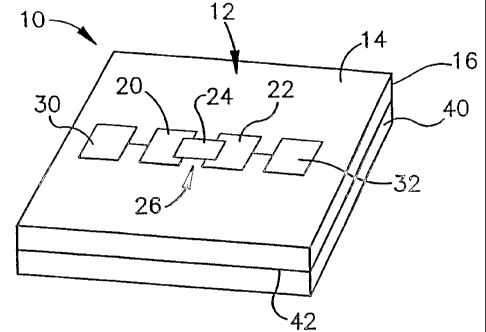
[~~~~~ Referring initially to Fig. 1, an RFID device 10 includes a
compensating
antenna configuration 12 on or atop a first face (major surface) 14 of a
dielectric
layer or substrate 16. The antenna configuration 12 includes a pair of antenna
elements (conductive tabs) 20 and 22, which are coupled to an RFID chip 24.
The RFID chip 24 may be part of an RFID strap 26, which for example includes
conductive leads atfiached to the RFID chip 24. Examples of suitable RFID
straps
include an RFID strap available from Alien Technologies, and the strap
marketed
under the name I-CONNECT, available from Philips Electronics.
[0060] The compensating antenna configuration 12 also includes antenna
compensation elements 30 and 32, which are coupled to or are a part of the
antenna elements 20 and 22. The compensation elements 30 and 32
compensate to some extent for changes in operating characteristics of the
antenna elements 20 and 22 due to the interaction of the antenna elements 20
and 22, and the dielectric material of the dielectric layer 16. The change in
operating characteristics of the antenna elements 20 and 22 may manifest
itself,
for example, the antenna elements 20 and 22 becoming reactive; the radiation
resistance of the antenna elements 20 and 22 changing, which may cause the
antenna efficiency, expressed as the ratio of radiation resistance to the sum
of
loss resistance and radiation resistance, to drop; and, as a result of the
above,
the impedance match between the RFID chip 24 and antenna elements 20 and
22 may degrade, leading to mismatch loss and hence loss of optimum frequency
operating range for the antenna structure. To mitigate these effects on the
antenna elements 20 and 22, the compensating elements 30 and 32 may: 1 )
introduce an impedance matching network between the chip and antenna which
impedance matches the two, maximizing power transfer between the chip 24 and
the antenna elements 20 and 22; and/or 2) change the effective length of the
antenna elements 20 and 22 so it stays at the resonant condition. These
methods may be used separately, or may be used in combination to form a hybrid
of the two. Various examples of compensating elements 30 and 32 are
discussed below.
CA 02522270 2005-10-07
WO 2004/093249 PCT/US2004/011147
{006'1] The RF1D ~i~vt~ce 1''0 also includes a conductive structure or ground
plane
40 on or atop a second major surface 42 of the dielectric layer 16 that is on
an
opposite side of the dielectric layer 16 than the first major surface 14. The
dielectric layer 16 is thus between the conductive structure 40 and the
antenna
configuration 12. The conductive structure or ground plane 40 provides a
"shield"
to reduce or eliminate sensitivity of the RFID chip 24 and fibs antenna
configuration 12 to objects on the other side of the ground plane 40. For
example, the ground plane 40 may be on the inside of a carton or container
that
contains one or more objects. The objects may have any of a variety of
properties that may affect operation of nearby unshielded RFID devices in
different ways. For example, elecfirically conductive objects within a
container,
such as metal objects or objects in metal wrappers, may affect operation of
nearby RFID devices differently than non-conductive objects. As another
example, objects with different dielectric constants may have different
effects on
nearby RFID devices. The presence of the ground plane 40 between the antenna
configuration 12 and RFID chip 24, and objects which may variably affect
operation of the RFID device, may aid in reducing or preventing interaction of
such objects and the working components of the RFID device 10.
[0062] The thickness or the dielectric characteristic of the dielectric layer
16 may
be selected so as to prevent undesired interaction between the ground plane 40
and the antenna configuration 12. Generally, it has been found that at UHF
frequencies, defined as a band in the range of 860 MHz to 950 MHz, a
dielectric
thickness of about 3 millimeters to 6 millimeters is suitable for a tag
embodying
the present invention. Likewise, a dielectric thickness of about 0.5
millimeter to
about 3 millimeters is suitable for a tag designed to operate in a band
centered on
2450 MHz. This range of thickness has been found to be suitable for efficient
operation of the conductive tabs 20 and 22, despite the normally believed
requirement for a separation distance of a quarter of a wavelength of the
operating frequency between the antenna configuration 12 and the ground plane
40.
[00~3j The ground plane 40 may be greater in extent fihan the operative parts
of
the RFID device 10 (the antenna configuration 12 and the RFID chip 24), so as
to
provide appropriate shielding to the operative parts of the RFID device 10.
For
example, the ground plane 40 may provide an overlap of the antenna
9
CA 02522270 2005-10-07
WO 2004/093249 PCT/US2004/011147
configuration "~~ o"~,a~ I~a~st about 6 mm in every direction. However, it may
be
possible to make do with less overlap in certain directions, for example
having
less overlap at distal ends of the antenna elements 20 and 22, farthest from
the
RFID chip 24, than at the width of the antenna elements 20 and 22.
[0054] The RFID device 10 may be employed in any of a variety of suitable
contexts. For example, the RFID device 10 may be a separate label affi~;ed to
a
carton or other container or object, for instance by being adhesively adhered
to
the carton. The label may be placed on one side of the carton or within the
object. Alternatively, one part of the RFID device may be adhesively attached
to
one side (one major face) of the carton (e.g., the ground plane attached to an
inside of the carton) and another part of the RFID device (e.g., operative
parts of
the RFID device) may be adhesively attached to the other side (other major
face)
of the carton. Indeed, as explained further below, the RFID device may be a
single label that wraps around an edge of a carton or other object, with the
one
part of the RFID device being on one part of the label, and the other part of
the
RFID device being on another part of the label, with part of the carton or
other
object being employed as a dielectric layer.
[0065] As another alternative, components of the RFID device 10 may be
directly formed on sides of an object or portion of an object, such as on
sides of a
portion of a carton or other object. For example the antenna configuration 12
may be printed or otherwise formed on one side of a part of a carton or other
object, and the ground plane 40 may be formed on a corresponding portion of an
opposite side of the carton or other object.
[0066] What follows now are generalized descriptions of various types of
compensation elements 30 and 32 that may be used as part of the compensation
antenna configuration 12. It will be appreciated that compensation elements
other that the precise types shown may be employed as the compensation
elements 30 and 32.
[0067] One general type of compensation element 30, 32 is a capacitor 50,
illustrated in Fig. 2. The capacitor 50 includes a pair of conductive plates
52 and
54 mounted or printed on a dielectric substrate 56. The capacitance between
these plates is a function of the separation, size and, importantly, the
dielectric
constant of the substrate. In general, as the relative dielectric constant (E~
)
increases, so will the capacitance C between the plates.
CA 02522270 2005-10-07
WO 2004/093249 PCT/US2004/011147
:r~b~$] ~pi~e spe~ific~~t~ype of capacitor that embodies the present invention
is
shown in Fig. 3. The capacitor 58 shown there is formed by the cross coupling
of
electromagnetic fields formed between the capacitor "fingers" 60 and 62 on a
dielectric 64. The capacitor 58 is referred to herein as an inter-digital
capacitor.
The capacitance and other characteristics of the capacitor 58 are generally a
function of the spacing between the fingers 50 and 6~, the number of fingers,
the
dimensions of the fingers 60 and 6~, and the dielectric constant of the
dielectric
material 64, on which the capacitor 58 is attached.
[009] Figs. 4 and 5 illustrate the electric field around the capacitor 58 for
two
different dielectric substrates 64. Fig. 4 shows the capacitor 58 on a
relatively
thin substrate 66, such as a 100p,m polyester layer. Fig. 5 shows the
capacitor 58
and the thin substrate 66 on a relatively thick substrate 68, such as a 30 mm
thick
dielectric block or slab having a dielectric constant between 2 and 7.
[0070] For the condition shown in Fig. 4, the inter-digital capacitor 58 is
essentially in air, with the dielectric constant between the alternate fingers
60 and
62 being that of the thin substrate 66. Capacitance between fingers of the
capacitor is a function of the dielectric constant around the fingers as the
electric
field spreads out, so it will have an initial value of C~.
[0071] In the condition in Fig. 5, the electric field also is flowing in the
block, and
hence there is cross coupling between fingers of the capacitor. The
capacitance
C2 is affected by the presence of the block, in particular by the dielectric
constant
of the material. Thus this arrangement comprises a component having a
capacitance (C) that is a function of the relative dielectric constant of the
block on
which it is mounted, i.e., C = f(Er), where Er is the relative dielectric
constant of
the block. As the dielectric constant of the block increases, the capacitance
increases. The component capacitance will also be a function of the block
thickness as a thinner block will have less of an electromagnetic field in it,
so will,
for a given Er, increase the capacitance by a lesser amount.
[0072] Fig. 6 illustrates one possible inductor structure, a spiral or meander
inducfior 69 having a number of turns or other parts (meanders) 70 in close
proximity to adjacent of the turns or other parts 70. This structure has a
self-
resonance, due to the capacitance between the turns. Hence the net inductance
value can also be made a function of substrate Er.
11
CA 02522270 2005-10-07
WO 2004/093249 PCT/US2004/011147
[~0~07~3] 1:n air, ~this~ meander inductor component will have a certain value
of
inductance, L. When it placed on higher dielectric constant materials of
significant thickness, the capacitive cross coupling between meanders
increases,
causing a reduction in overall inductance.
[0074] Fig. 7 is a simplified illustration of how meander inductor components
are
used. A dipole antenna 78 with elemenfs 80 is connected to an o~Fl~ chip 82
through meander inductors 84. The antenna 78, the inductors 84, and the chip
82 are attached to a thin dielectric material 86 (more precisely, a low
dielectric
constant substrate such as a 100 p,m-thick polyester film) by being printed
thereon, glued thereto, or mounted thereon in any of the customary ways.
[0075] Fig. 8 illustrates another configuration using the meander inductors
84,
added between the dipole antenna 78 and chip 82. The dipole antenna 78, the
chip 82, and the meander inductors 84 are all on a higher dielectric constant
substrate 88.
[0076] If the basic dipole antenna 78 is sized for placement in air or on a
low
dielectric constant Er substrate, when the dipole antenna 78 is placed on a
higher
dielectric constant Er substrate 88, the antenna elements are too long at the
chosen operating frequency. This manifests itself primarily by the antenna
becoming inductive, that is, +jX increasing. Without compensation between the
antenna 78 and the chip 82, the impedance match and hence tag performance
would degrade. However, the meander inductors 84 have reduced the
inductance on the higher dielectric constant Er substrate 88. The meander
inductors 84 on the substrate 88 thus provide a smaller +jX to the circuit, so
with
proper selection of characteristics a good impedance match is maintained.
[0077] The single capacitive and inductive elements discussed above show the
principle of a component's value being dependant on the characteristics of the
substrate on which it is placed. A number of other components, which can be
formed on a film next to an antenna that will react to the varying dielectric
constant of the substrate material and its thickness, can be made, including
multiple capacitors, inductors and transmission line elements (which can act
as
firansformers), acting in parallel or series with one another to provide a
substrate-
dependant variable reactance. These substrate-dependant variable-reactance
components can be used to re-tune and re-mafich the antenna l chip
combinafiion,
12
CA 02522270 2005-10-07
WO 2004/093249 PCT/US2004/011147
to mai~ta~Gn p~rforr~ana~ for some antenna types over a certain range of
substrate
characteristics.
[0078] From the foregoing it has been established that surface features of a
structure can react to or interact with the substrate upon which they are
mounted,
changing operating characteristics depending upon local environment,
particularly
upon the dielectric characfier of the substrate. However, using these
components
alone is nofi always the best solution. f~nofiher approach for fibs
compensation
elemenfis 30 and 32 is for sfiructures which change the effective length of
antenna
based on the environment in the vicinity of the compensation elemenfis,
particularly based on dielectric characterisfiics of the dielectric mafierial
upon
which fibs compensation elements 30 and 32 are mounfied. Some simple
structures and methods of changing the effective length of antenna elements
are
now described.
[00'19] For this purpose, one of the simplest antennas to consider will be a
folded dipole 100, as illustrated as part of an RFID device 102, in Fig. 9.
The total
length of the loop 104 of the folded dipole antenna 100 is set to provide a
good
match to an RFID chip 105 at the minimum dielectric constant the tag is
designed
to operate with, as an example, a 30mm block having a dielectric constant of
Er =
2.
[0080] The adaptive elements 106 may include a printed series tuned circuit,
consisting of an inductor, which is a simple meander of narrow line, and an
inter-
digital capacitor as discussed and illustrated previously. The value of the
inductor
and capacitor is such that, on materials having a dielectric constant of Er=
2, the
resonance frequency is above 915MHz, as the capacitor value is low. If the
complete tag is placed on a 30mm substrate having a dielectric constant of E~=
4,
the correct length of the loop for the folded dipole is now shorter. However,
the
capacitor inside the adaptive element 106 may have increased in value, making
the loop resonant at 915MHz. The adaptive capacitive element now acts like a
short circuit, providing a reduced length path for the RF current which is
ideally
exactly the path length to make the antenna correctly matched fio the chip on
materials having a dielectric constant of Er= 4. Ifi will be appreciated thafi
fibs
values and numbers in the examples are intended for explaining general
principles of operafiion, and do not necessarily represent real antenna and
RFID
tags designs.
13
CA 02522270 2005-10-07
WO 2004/093249 PCT/US2004/011147
[0081]' This is ~n example, using substrate properties as embodied in the
present
invention to adapt the effective length of an antenna. Alternately,
distributed
versions can be envisaged, where the inductance and capacitance are spread
along the antenna length. It will appreciated that these capacitive and
inductive
elements may be used in series and/or parallel combinations and may
potentially,
combined with a antenna having appropriafie characteristics, allow the
impedance
match to be adjusted as the substrate E~ varies, to allow the antenna
performance
to be maintained.
[0082] An alternative structure is one where the compensating elements 30 and
32, such as the adaptive elements 106, adjust the effective length of the
antenna.
UVhen an antenna is placed on or in a medium of a different Er, the wavelength
of
a defined frequency changes. The ideal length for that antenna in the medium,
to
obtain a low or zero reactance and useful radiation resistance, would be
shorter.
[0083] Therefore an antenna that reduces its effective length as the substrate
dielectric constant varies would provide compensation. A concept for a
structure
that can achieve this is shown below in Fig. 10. This is a non-limiting
example as
a number of other suitable configurations are possible using various of the
structures and methods described herein, alone or in combination with one
another.
[0084] Fig. 10 is a plan view showing a curved section of a rectangular cross
section conductor 116 designed to be placed on a substrate having any of a
variety of values of Er. This would form part of the two arms of a dipole
antenna.
More than one section may be used. The conductor 116 has potentially two
paths for the current to flow: an outer curve 118 and an inner curve 120. The
length of the transmission path is actually different between these two
curves.
The slit 122 acts as a capacitor. As the substrate Er increases in its
dielectric
constant value, the capacitance between the two radiating sections likewise
increases, but the effective transmission path decreases in length.
[0085] It will be appreciated that many alternatives are possible for
providing
adaptive structures that are configured fio compensate to some extent for
different
values of dielectric constant in a substrate to which the adaptive or
compensating
antenna structure is attached. For example, cross coupling between a simple
wave format structure could also be designed to provide compensafiion. Cross
coupled structures have been described above.
14
CA 02522270 2005-10-07
WO 2004/093249 PCT/US2004/011147
~.~a8~6'] Fig. 14 shows a°n avtenna structure 140 that includes some
adaptive
elements that are examples of compensating elements of some of the types
discussed above. The antenna structure 140 includes a pair of antenna elements
142 and 144 that are coupled to an RFI~ chip or strap at respective attach
points
146 and 148. The antenna elements 142 and 144 have respective main antenna
lines 152 and 154. At the end of the main antenna lines 152 and 154 are
capacitive stubs 156 and 158. The capacitive stubs 156 and 158 include
respective conductive tails 162 and 164 that bend back toward the
corresponding
main antenna lines 152 and 154. Gaps 166 and 108 between the conductive tails
162 and 164, and the main antenna lines 152 and 154, widen further with
further
distance from the joinder of the conductive tails and the main antenna lines.
The
capacitive stubs 156 and 158 have variable characteristics, depending on the
dielectric constant of the substrate to which the antenna structure 140 is
attached.
More particularly, the capacitance between the conductive tails 162 and 164
and
the main antenna lines 152 and 154, respectively, is a function of the
dielectric
constant of the substrate material upon which the antenna structure 140 is
mounted.
[0087] The antenna structure 140 also includes loop lines 172 and 174 on
either
side of the main antenna lines 152 and 154. As shown, the loop lines 172 and
174 are narrower than the main antenna lines 152 and 154. Each of the loop
lines 172 and 174 is coupled to both of the main antenna lines 152 and 154.
There is a gap 182 between the loop line 172 and the main antenna lines 152
and
154. A corresponding gap 184 is between the loop line 174 and the main
antenna lines 152 and 154. The gaps 182 and 184 have variable thickness,
being narrow where the loop lines 172 and 174 join with the main antenna lines
152 and 154, and widening out toward the middle of the loop lines 172 and 174.
The loop lines 172 and 174 function as inductors in the absence of a ground
plane on an opposite side of the dielectric substrate layer. With a ground
plane,
such as the ground plane 40 (Fig. 1 ) described above, on the other side of
the
dielectric layer, the loop lines 172 and 174 may function as microstrip lines,
improving the impedance match between the antenna structure 140 and the RFI~
chip or strap coupled to the antenna structure 140.
[0088] Fig. 12 shows an alternate antenna structure 200 having a pair of
generally triangular antenna elements (conductive tabs) 202 and 204. The
CA 02522270 2005-10-07
WO 2004/093249 PCT/US2004/011147
antenna elements 202 and 204 have attachment points 206 and 208 for coupling
an RFID chip or strap to the antenna structure 200.
[0089] The antenna elements 202 and 204 have respective compensation or
adaptive portions or elements 212 and 214. The adaptive portions 212 and 214
provide gaps 216 and 218 in the generally triangular conductive tabs. ~n one
side of the gap 218 is a conductive link 220, including a relatively wide
central
portion 222, and a pair of relatively narrow portions 224 and 226 along the
sides
of the gap 216, coupling the central portion 222 to the parts 228 and 230 of
the
antenna element 202 on either side of the gap 216. The central porfiion 222
may
have a width appro~zimately the same as that of the antenna element parts 228
and 230 in the vicinity of the gap 216. The narrow portions 224 and 226 may be
narrower than the central portion 222 and substantially all of the antenna
element
parts 228 and 230. The antenna element 204 may have a conductive link 234,
substantially identical to the conductive link 220, in the vicinity of fihe
gap 218.
[0090] The antenna structure 200 has been found to give good performance
when mounted on walls of cardboard cartons filled with a variety of different
products containing both conductive and non-conductive materials. The antenna
structure 200, and in particular the adaptive portions 212 and 214, may
provide
compensation for various environments encountered by the antenna structure
200, for example including variations in substrate characteristics and
variations in
characteristics of nearby objects. The antenna structure 200 may be used with
or
without a conductive structure or ground plane on an opposite side of a
dielectric
substrate, such as a cardboard carton wall, to which the antenna structure is
mounted. For example, the antenna structure 200 may be mounted onto a
cardboard container 3-4 mm thick.
[0091] As discussed above, the various adaptive or compensating antenna
structures described herein may be employed with an overlapping ground plane
for use providing some measure of shielding, to at least reduce the effect of
nearby objects on operations of RFID devices containing the antenna
structures.
However, it will be appreciated that some or all of the antenna structures may
be
used without a corresponding ground plane.
[0092 Vllhat is now described are various configurations involving conductive
structures such as ground planes. Also described are some configurations of
antenna elements (conductive tabs) that have been found to be effective in
16
CA 02522270 2005-10-07
WO 2004/093249 PCT/US2004/011147
cornbi~iati~'h v~e~thi grour~~ pt~nes, although it will be appreciated that
other
configurations of antenna elements may be used with ground planes. It will be
appreciated that the above-described adaptive elements may be suitably
combined with the below-described ground planes, methods and configurations.
[009] As an overview, a radio frequency identification device (RFID) and its
antenna system may be attached to a package or confiainer fio communicate
information about the package or container to an external reader. The package
may be an individual package containing specific, known contents, or an
individual, exterior package containing within ii a group of additional,
interior
individual packages. The word "package" and "container" are used
interchangeably herein to describe a material that houses contents, such as
goods or other individual packages, and equivalent structures. The present
invention should not be limited to any particular meaning or method when
either
"package" or ''container" is used.
[0094] As noted above, an RFID device may include conductive tabs and a
conductive structure, with a dielectric layer between the conductive tabs and
the
conductive structure. The conductive structure overlaps the conductive tabs
and
acts as a shield, allowing the device to be at least somewhat insensitive to
the
surface upon which it is mounted, or to the presence of nearby objects, such
as
goods in a carton or other container that includes fihe device. The dielectric
layer
may be a portion of the container, such as an overlapped portion of the
container.
Alternatively, the dielectric layer may be a separate layer, which may vary in
thickness, allowing one of the conductive tabs to be capacitively coupled to
the
conductive structure. As another alternative, the dielectric layer may be an
expandable substrate that may be expanded after fabrication operations, such
as
printing.
(0095] Fig. 13 illustrates an RFID tag 410 that includes a wireless
communication device 416. The device 416 may be either active in generating
itself the radio frequency energy in response to a received command, or
passive
in merely reflecting received radio frequency energy back to an external
originating source, such as current RFID tag readers known in the art.
[0096] In this embodiment, there are at least two conductive tabs 412 and 414,
coupled to the wireless communication device for receiving and radiating radio
frequency energy received. The tabs 412 and 414 together form an antenna
17
CA 02522270 2005-10-07
WO 2004/093249 PCT/US2004/011147
structure ~.'~1 ~, Tlie tvro~tabs 412 and 414 are substantially identical in
shape and
are coupled to the wireless communication device 416 at respective feedpoints
420 and 422 that differ in location relative to each of the tabs 412 and 414.
The
tabs 412 and 414 may be generally identical in conducting area if the two tabs
are
of the same sire as well as shape. Alternatively the tabs 412 and 414 may
differ
in sire while their shape remains generally the same resulting in a different
conducting area. The tabs 412 and x.14 may be collinear or non-collinear to
provide different desired antenna structures. For example, in Fig. 13 fiabs
412
and 414 are offset and adjacent to provide a slot antenna system in area 418
that
provides for resonance at multiple radiating frequencies for operation at
multiple
frequencies.
[0097] It is also contemplated that the invention includes having multiple
arrays
of conductive tabs that are connected to device 416. These tabs may be
designed to work in unison with one another to form dipole or Yagi antenna
systems, or singly to form monopole antennas as desired for the particular tag
application. By using such multiple conductive tab arrays, mulfiiple resonant
frequencies may be provided so that the tag may be responsive to a wider range
of tag readers and environmental situations than a single dedicated pair of
conductive tabs.
[0098] Other considered shapes for the conductive tabs are illustrated in
Figs.
14 and 15, and include not only regular shapes such as the tapered, triangular
shape illustrated in Fig. 13, but also truncated triangular shapes denoted by
reference numbers 432 and 434 in Fig. 15.
[0099] Rectangular shaped conductive tabs are also included in this invention
as illustrated in Fig. 14 as reference numbers 422 and 424. In fact, Fig. 14
illustrates, for example, that the tabs may include a series of contiguous
rectangular portions 426, 427, 428 and 440, 441, 442.
[0100] In one embodiment of the invention, the rectangular portions shown in
Fig. 14 will have dimensions substantially as follows: Rectangular portion 426
is
about 3 millimeters wide by about 3 millimeters long; contiguous rectangular
portion 427 is about 10 millimeters wide by about 107.6 millimeters long; and,
rectangular portion 428 is about 3 millimeters wide by 15.4 millimeters long.
With
these dimensions, ifi is further preferred that the dielectric substrafie have
a
thickness between the conductive tabs and the ground plane of about 6.2
18
CA 02522270 2005-10-07
WO 2004/093249 PCT/US2004/011147
millimeters for "foa~rn. ~~~Kew~se, the ground plane for this preferred
embodiment is
about 16 millimeters wide by about 261 millimeters long.
[0101] The conductive tabs may also have irregular shapes, or even composite
shapes that include both regular and irregular portions. Other alternative
antenna
systems that embody the present invention include those that have tabs with a
triangular portion contiguous with a freeform curve or a regular curve such
ass a
sinusoidal pattern.
[0102] In Fig. 13, the tab feedpoints 420 and 422, may be selected so that the
impedance across the two feedpoints 420 and 422 of tabs 412 and 414,
respectively, is a conjugate match of the impedance across the wireless
communication device 416 to allow for a maximum transfer of energy
therebetween.
[0103] In general, a method of selecting feedpoints on the tabs to achieve
this
conjugate impedance match, may be to select points on each tab differing in
location where the width profile of each tab, taken along an axis transverse
to the
longitudinal centerline axis of each tab, differs from one another. That is,
the
feedpoints 420 and 422 may be selected such that the width of the tabs 412 and
414 at the feedpoints 420 and 422, taken along the centerline of the tab as
you
move away from the center of the tag where it connects to the communications
device, measured against the length, differs between the two tabs 412 and 414.
By choosing such points, either by calculation or trial and error, a conjugate
impedance match can be achieved.
[0104] Specifically, with reference to the Figures, the longitudinal
centerline axis
of a tab is seen to be a line that remains equidistant from opposite borders
or
edges of the tab and extending from one end of the tab to the other. At times
with
regular shaped tabs, this longitudinal centerline axis will be a straight line
similar
to a longitudinal axis of the tab. At other times, with irregular shaped tabs,
the
longitudinal centerline axis will curve to remain equidistant from the
borders. It is
also seen that this longitudinal centerline axis is unique to each tab. The
width of
the tab is determined along an axis transverse to the longitudinal centerline
axis
and will be seen to be dependent upon the shape of the tab. For example, with
a
rectangular shaped tab, the width will not vary along the longitudinal
centerline
axis, but with a triangular or wedge shaped tab, fihe width will vary
continuously
along the longitudinal centerline axis of the tab. Thus, while it is
contemplated
19
CA 02522270 2005-10-07
WO 2004/093249 PCT/US2004/011147
,t#~at,.th'~ prese~rt'inv~entibi~ ir~'~ludes tabs having rectangular shaped
portions, there
will also be portions having different widths.
[0105] Another method of selecting the feedpoints on the conductive tabs, is
to
select a feedpoint differing in location on each of the tabs where the
conducting
area per unit length of the longitudinal centerline axis of each tab varies
with
distance along the longitudinal centerline a~zis of each of said tabs from its
feedpoint. In essence, this method selects as a feedpoint a location on each
tab
where the integrated area of the shape per unit length of the centerline
varies and
is not necessarily the width of the tab.
[0106] Fig. ~ 6 illustrates how a radio frequency reflecting structure or
ground
plane 450 is operatively coupled to tabs 452 and 454, for reflecting radio
frequency energy radiated from the tabs 452 and 454. The ground plane
elements may be substantially the same size as the conductive tabs or greater,
so that the ground plane elements may effectively reflect radio frequency
energy.
If the ground plane elements are substantially smaller than the conductive
tabs,
the radio frequency energy will extend beyond the edges of the ground plane
elements and interact with the contents of the packaging causing deterioration
in
the operating efficiency of the label. In one embodiment, the ground plane 450
may extend at least about 6 mm beyond the boundary of the tabs 452 and 454.
[0107] in the illustrated embodiment the wireless communication device 456 is
connected at feedpoints 458 and 460 to the tabs 452 and 454. This structure
450
may be a simple ground plane made from a single, unitary plate or a complex
reflecting structure that includes several isolated plates that act together
to reflect
radio frequency energy. If the antenna structure is located on one side of a
package wall 462, the radio frequency reflecting structure 450 may be on the
opposite side of the same wall 462 using the wall itself as a dielectric
material as
described further below.
[0108] As indicated above, a dielectric material is preferably located
intermediate the conductive tabs 452 and 454, and the radio frequency
reflecting
structure 450. An example of such a dielectric material is the packaging wall
462
described above. The thickness or the dielectric characteristic of the
dielectric
intermediate the tabs and radio frequency reflecting structure may be varied
along a longitudinal or transverse axis of the tabs. Generally, it has been
found
that at UHF frequencies, defined as a band in the range of 860 MHz to 950 MHz,
CA 02522270 2005-10-07
WO 2004/093249 PCT/US2004/011147
a dielectric thickness of a~b~ovt 3 millimefiers to 6 millimeters is suitable
for a tag
embodying the present invention. Likewise, a dielectric thickness of about 0.5
millimeter to about 3 millimeters is suitable for a tag designed to operate in
a
band centered on 2450 MHz. This range of thickness has been found to be
suitable for efficient operation of the conductive tabs despite the normally
believed requirement for a separation distance of a quarter of a wavelength of
the
operating frequency between the radiating element and ground plane.
[0109] With the present invention advantages have been found in both
manufacturing and application of the labels in that a thinner, lower
dielectric
material may be used in label construction, as wail as the fact that shorter
tabs
may be utilized resulting in a manufacturing savings in using less ink and
label
materials in constructing each label and in increasing the label density on
the web
medium during manufacturing making less wasted web medium. Also such
thinner and smaller labels are easier to affix to packaging and less likely to
be
damaged than those thicker labels that protrude outwardly from the packaging
surface to which they are attached.
[0110] Another embodiment is directed toward the antenna structure itself as
described above without the wireless communication device.
[0111] Fig. 17 illustrates an RFID device 500 configured to be placed over the
edge of an object, such as the edge of a cardboard carton. The RFID device 500
is a label in two sections 502 and 504, with a boundary 506 therebetween. The
sections 502 and 504 may include a single substrate 508, which may have a
suitable adhesive backing, such as a suitable pressure-sensitive adhesive.
[0112] The firsfi section 502 has a conductive ground plane 510 printed or
otherwise formed upon the substrate 508. The ground plane 510 may be formed
from conductive ink.
[0113] The second section 504 includes an antenna structure 520 printed or
formed on the substrate 508, and an RFID chip or strap 522 coupled to the
antenna structure 520. The antenna structure 520 may include antenna elements
524 and 526, which may be similar to the antenna elements (conductive tabs)
discussed above, and adaptive or compensating elements 530 and 532. The
adaptive or compensating elements 530 and 532 may include one or more of the
types of adaptive or compensating elements discussed above.
21
CA 02522270 2005-10-07
WO 2004/093249 PCT/US2004/011147
~'0~11~~j 'F~i~.s. ~~i~8 and 1>;9 r~~ustrate installation of the RFID device
500 on a panel
540 of an object 542, such as a cardboard container. The RFID device 500 is
folded over an edge 544 of the panel 540, with the first section 502 on the
inside
of the panel 540 and the second section 504 on the outside of the panel 540.
The boundary 506 between the two sections 502 and 504 is approximately placed
along the edge 544 of the panel 540. Since the RFID device 500 is on a single
subsfirate 508, folding the device 500 to place the sections 502 and 504. on
opposite sides of the panel 540 provides some measure of alignment between
the ground plane 510 and the antenna structure 520. It will be appreciated
that
the ground plane 510 may have an increased amount of overlap to compensate
for possible misalignment between the ground plane 510 and the antenna
structure 520 in the adhering of the RFID device 500 to the panel 540.
[0115] The adaptive elements 530 and 532 may provide compensation for
variations that may be encountered in the objects the RFID device 500 is
applied
to. Such variations may be due, for example, to variations in container
material
thickness andlor dielectric characteristics.
[0116] It will be appreciated that many variations are possible for the
configuration of the RFID device 500. For example, it may be possible to
utilize
other types of antenna elements, described below and above, as an alternative
to
the triangular antenna elements 524 and 526.
[0117] Turning now to Fig. 20, an RFID device 670 is illustrated mounted on
parts 672 and 674 of a carton 676. The device 670 is located on an overlapping
portion 680 of the carton 676, where the parts 672 and 674 overlap one
another.
The parts 672 and 674 may be adhesively joined in the overlapping portion.
Alternatively, the parts 672 and 674 of the carton 676 may be joined by other
means, such as suitable staples or other fasteners. On one side or major face
678 of the overlapping portion 680 are conductive tabs 682 and 684, and a
wireless communication device 686, such as an RFID chip or strap. A radio
frequency reflecting structure or ground plane 690 is on an opposite side or
major
face 692 of the overlapping portion 680.
[p118] The overlapping portion 680 of the carton 676 thus functions as a
dielectric between the conductive tabs 682 and 684, and the wireless
communication device 686. PerFormance of the RFID device 670 may be
enhanced by the additional thickness of the overlapping portion 680, relative
to
22
CA 02522270 2005-10-07
WO 2004/093249 PCT/US2004/011147
.l~:irig~e~~~hE~~~~vs'(r~oi~-o~r~~l~pped) parts of the carton parts 672 and
674. More
particularly, utilizing a double-thickness overlapped carton portion as the
dielectric
for an RFID device may allow for use of such devices on cardboard cartons
having thinner material. For example, some cartons utilize a very thin
cardboard,
such as 2 mm thick cardboard. A single thickness of 2 mm thick cardboard may
be unsuitable or less suitable for use with surface-insensitive RFID device
such
as described herein.
[0119] The RFID device 670 shown in Fig. 20 may be produced by printing
conductive ink on the opposite sides (major faces) 678 and 692 of the
overlapping portion 680, to form the conducfiive tabs 682 and 684, and the
reflecting sfiructure 690. It will be appreciated that a variety of suitable
printing
methods may be used to form the tabs 682 and 684, and the reflecting structure
90, including ink jet printing, offset printing, and Gravure printing.
[0120] The wireless communication device 686 may be suitably joined to the
conductive tabs 682 and 684 following printing of the conductive tabs 682 and
684. The joining may be accomplished by a suitable roll process, for example,
by
placing the communication device 686 from a web of devices onto the tabs 682
and 684.
[0121] It will appreciated that the printing may be performed before the
carton
parts 672 and 674 are overlapped to form the overlapping portion 680, or
alternatively that the printing may in whole or in part be performed after
formation
of the overlapping portion 680. The conductive ink may be any of a variety of
suitable inks, including inks containing metal particles, such as silver
particles.
[0122] It will be appreciated that formation of the conductive tabs 682 and
684,
and/or the reflective structure 690 may occur during formation of the carton
parts
672 and 674, with the conductive tabs 682 and 684 and/or the reflective
structure
690 being for example within the carton parts 672 and 674. Forming parts of
the
RFID device 670 at least partially within the carton parts 672 and 674 aids in
physically protecting components of the RFID device 670 from damage. In
addition, burying some components of the RFID device 670 aids in preventing
removal or disabling of the RFID device 670, since the RFID device 670 may
thereby be more difficult to locate.
[0123] In one embodiment, the conductive tabs 682 and 684 may be printed
onto the interior of the carton parts 672. As illustrated in Fig. 21, a marker
696
23
CA 02522270 2005-10-07
WO 2004/093249 PCT/US2004/011147
i!rn~y.~e~~p~rmte~awr~~t~eraw~~~eapiaced on one of the carton parts 672 and
674 to
indicate where the reflective structure 690 is subsequently to be placed.
(0124] The conductive tabs 682 and 684 may have any of the suitable shapes or
forms described herein. Alternatively, the conductive tabs 682 and 684 may
have
other forms, such as shapes that are asymmetric with one another. The
conductive tabs 682 and 684 may have configurations that are tunable or
otherwise compensate for different substrate materials and/or thicknesses,
and/or
for other differences in the environment encountered by the RFID device 670,
such as difFerences in the types of contents in a carton or ofiher container
on
which the RFID device 670 is mounted.
(0125] The RFID devices 670 illustrated in Figs. 20 and 21 enable mounting of
devices on a wider range of packaging materials, with the reflective structure
690
providing a "shield" to reduce or prevent changes in operation of the RFID
device
670 due to differences in the types of merchandise or other material stored in
a
carton or other container upon which the RFID device 670 is mounted. As
illustrated in Fig. 23, the RFID device 670 may be located on a carton or
other
container 698, oriented so that the reflective structure 690 is interposed
between
the conductive tabs 682 and 684, and the interior of the container 698.
(0126] Fig. 23 shows the operative components of another embodiment RFID
device, an RFID device 700 having an essentially monopole antenna structure
702. The RFID device 700 includes a wireless communication device 706 (e.g., a
strap) that is coupled to a pair of conductive tabs 708 and 710 that are
mounted
on a substrate 712, with a reflective structure or ground plane 714 on an
opposite
side of the substrate 712 from the conductive tabs 708 and 710.
(0127] At least part of one of the conductive tab 708 is capacitively coupled
to
the reflective structure 714, by being mounted on a thinner portion 716 of the
substrate 712, which has a thickness less than that of the portion of the
substrate
712 underlying the conductive tab 710. It will be appreciated that, with
proper
attention to matching, electrically coupling the tab 708 to the conductive
reflective
structure 714, allows operation of the RFID device 700 as a monopole antenna
device. The relative thinness of the thinner portion 716 facilitates
capacitive
electrical coupling between the conductive tab 708 and the conductive
reflective
structure 714.
24
CA 02522270 2005-10-07
WO 2004/093249 PCT/US2004/011147
~b~!'~2"g~~~.a~"~~:~1~~~~li~~Ct~~~l..f~~i~~~~110 functions as a monopole
antenna element. The
conductive tab 710 may have a varying width, such as that described above with
regard to other embodiments.
[0129] The matching referred to above may include making the relative
impedances of the antenna structure 102 and the wireless communication device
106 complex conjugates of one another. In general, the impedance of the
antenna structure 102 will be a series combination of various impedances of
the
RFI~ device 100, including the impedance of the conductive tab 108 and its
capacitive coupling with the reflective structure 114.
[0~ 30] The thinner portion 716 may be made thinner by inelastically
compressing the material of the substrate 712. For example the substrate 712
may be made of a suitable foam material, such as a suitable thermoplastic foam
material, which may be a foam material including polypropylene and/or
polystyrene. A portion of the substrate 712 may be compressed by applying
sufficient pressure to rupture cells, causing the gas in the cells to be
pressed out
of the foam, thereby permanently compressing the foam.
[0131 ] The compressing described above may be performed after the formation
of the tabs 708 and 710 on the substrate 712. The pressure on the tab 708 and
the portion of the substrate 712 may be directed downward and sideways, toward
the center of the RFID device 700, for example where the wireless
communication device 706 is mounted. By pressing down and in on the
conductive tab 708 and the substrate 712, less stretching of the material of
the
conductive tab 708 occurs. This puts less stress on the material of the
conductive
tab 708, and may aid in maintaining integrity of the material of the
conductive tab
708.
[0132] As an alternative, it will be appreciated that the conductive tabs 708
and
710 may be formed after compression or other thinning processes to produce the
thinned portion 716 of the substrate 712. The conductive tabs 708 and 710 may
be formed by suitable processes for depositing conductive material, such as by
printing conductive ink.
[0133] Vllith reference again fio Fig. 23, the substrate 712 may have a sloped
region 720 between its thicker portion 722 and the thinner portion 716. The
sloped region 720 may aid in reducing stresses on the conductive tab 708 when
the conductive tab 708 is placed prior to compressing of the thinner portion
716,
CA 02522270 2005-10-07
WO 2004/093249 PCT/US2004/011147
~byafn~c~~~~~ne~"t'n~ a~~ea~c~tvtrt~ conductive tab 708 that is under stress.
When the
thinner portion 716 is compressed prior to printing or other depositing of the
conductive tab 708, the sloped region 720 may aid in ensuring conduction
between a first part 732 of the conductive tab 708 that is on the thicker
portion
722 of the substrate 712, and a second part 736 of the conductive tab 708 that
is
on the thinner portion 716 of the substrate 712.
[~'i34] It will be appreciated that a variety of suitable methods may be
utilized to
produce the thinner portion 716 of the substrate 712. In addition to the
compressing already mentioned above, it may be possible to heat a portion of
the
substrate, either in combination with compression or alone, to produce the
thinner
porfiion 716. For example, a thermoplastic foam material may be heated and
compressed by running it through a pair of rollers, at least one of which is
heated.
The thermoplastic film may be compressed over an area, and turned into a solid
thermoplastic sheet, thus both reducing its thickness and increasing its
dielectric
constant. Alternatively, material may be removed from a portion of the
substrate
712, by any of a variety of suitable methods, to produce the thinner portion
716.
[0135] As suggested above, the proximity of the second conductive tab part 736
to the conducting reflective structure 714, with only the thinner portion 716
of the
substrate 712 between, aids in capacitively coupling the second part 736 and
the
reflective structure 714. In a specific example, a 3.2 mm thick foam
dielectric was
compressed over a 20 mm x 10 mm area, to a thickness of 0.4 mm. This raised
the dielectric constant of the plastic foam material from 1.2 to 2.2.
Therefore, due
to the reduced thickness of the foam and the increased dielectric constant of
the
substrate material in the thinner portion 716, the total capacitance was
increased
from 0.66 pF to 9.7 pF, which has a reactance of 17.8 ohms at 915 MHz.
[0136] With reference now to Fig. 24, the RFID device 700 may include a
compressed border or ridge edge 740 substantially fully surrounding the device
700. Part of the compressed ridge edge 740 serves as the thinner portion 716
for
capacitively coupling the second part 736 of the conductive tab 708 to the
reflective structure 714. The remainder of the compressed ridge edge 740 may
serve a mechanical structural function, providing a rigid edge to the RFID
device
700 to prevent flexing of the RFID device 700.
[013'] Another embodiment of the RFID device 700 is illusfirated in Fig. 25.
The
RFID device in Fig. 25 includes a resonator (a conductive tab) 750 with a
26
CA 02522270 2005-10-07
WO 2004/093249 PCT/US2004/011147
oa ~~ a~cit~i've~ g~r~aund ~~5~2 ~~t°t~n~e end. The wireless
communication device 706 is
coupled to the resonator 750 at a suitable impedance point. The wireless
communication device 706 is also coupled to a capacitive ground 754. The
connection point between the wireless communication device 706 and the
resonat~r 750 may be selected t~ suitably match impedances of the wireless
communication device 706 and the active part ~f the resonator 750.
[O~i38] The RFID devices 700 illustrated in Figs. 23-25 may be suitable for
use
as labels, such as for placement on cartons containing any of a variety of
suitable
materials. The RFID devices 700 may include other suitable layers, for example
an adhesive layer for mounting the RFID device 700 on a carton, another type
of
container, or another object.
[0139] The RFID device 700 may be produced using suitable roll operations.
Fig. 26 shows a schematic diagram of a system 760 for making RFID devices,
such as the RFID device 700. Beginning with a roll 762 of a substrate material
764, a suitable printer 766 prints the conductive tabs 708 and 710 (Fig. 23)
and
the reflective structure 714 (Fig. 23) on opposite sides of the substrate
material
764. It will be appreciated that the printer 766 may actually include multiple
printers, for example to print the conductive tabs in a separate operation
from the
printing of the reflective structure.
[0140] A placement station 768 may be used to place the wireless
communication devices 706 (Fig. 23), such as straps. The wireless
communication devices 706 may be transferred to the substrate material 764
from
a separate web of material 770. Alternatively, it will be appreciated that
other
methods may be used to couple the wireless communication devices 706 to the
substrate material 764. For example, a suitable pick-and-place operation may
be
used to place the wireless communication devices 706.
[0141] Finally, the substrate material 764 is passed between a pair of rollers
774
and 776. The rollers 774 and 776 may be suitably heated, and have suitably-
shaped surfaces, for example including suitable protrusions and/or recesses,
so
as to compress a portion of the substrate material 764, and to separate the
RFID
devices 700 one from anofiher. In addition, a protective surface sheet 778 may
be
laminated onto the sheet material 764, to provide a protective top surface for
the
RIFD devices 700. It will be appreciated that the compressing, laminating, and
cutting operations may be performed in separate steps, if desired.
27
CA 02522270 2005-10-07
WO 2004/093249 PCT/US2004/011147
Co~4a] ~Itwill be a~~preciated that other suitable processes may be used in
fabricating the RFID devices 700. For example, suitable coating techniques,
such
as roll coating or spray coating, may be utilized for coating one side of the
devices with an adhesive, to facilitate adhering the RFID devices to cartons
or
other confiainers.
[~~4~] The RFID device 700, wifih ifis monopole anfienna strucfiure 702, has
fihe
advanfiage of a smaller size, when compared with similar devices having dipole
antenna structures. The length of the tag can be nearly halved with use of a
monopole antenna, such as in the device 700, in comparison to a dipole
antennaed device having similar size of antenna elemenfis (conducfiive tabs).
~y
having RFID devices of a smaller size, it will be appreciated that such
devices
may be utilized in a wider variety of applications.
[0144] Fig. 27 shows an RFID device 780 having an expandable substrate 782,
which can be maintained during manufacturing and processing operations with a
reduced thickness. The reduced thickness, which may be from about 0.05mm to
0.5mm, may advantageously allow the RFID device 780 to pass through standard
printers, for example to print a bar code or other information on a label 784
that is
part of the RFID device 780. After performing operations that take advantage
of
the reduced thicknesses of the substrate 782, the substrate 782 may be
expanded, increasing its thickness to that shown in Fig. 27.
[0145] The RFID device 780 has many of the components of other of the RFID
devices described herein, including a wireless communication device 786 and a
pair of conductive tabs 788 and 790 on one side of the substrate 782, and a
reflective structure (conductive ground plane) 792 on the other side of the
substrate 782.
[0146] Referring now in addition to Figs. 28-30, details of the structure of
the
expandable substrate 782 are now given. The expandable substrate 782
includes a top layer 802, a middle layer 804, and a bottom layer 806. The
middle
layer 804 is scored so as to be separafied into segments 808, 810, and 812, as
a
shear force is applied to the top layer 802 relative to the bottom layer 806.
The
segmenfis 808, 810, and 812 are in turn scored on fold lines, such as the fold
lines 818 and 820 of the segment 808. The scoring along the fold lines 818
allows parts 822, 824, and 826 of the segment 808 to fold relative to one
another
as shear force is applied between the top layer 802 and the bottom layer 806.
28
CA 02522270 2005-10-07
WO 2004/093249 PCT/US2004/011147
[0147] F~ach o~f'tE~e segments 808, 810, and 812 has three parts. The top
layer
802 has adhesive pads 832 selectively applied to adhere the bottom layer 802
to
the parts on one side of the segments 808, 810, and 812 (the rightmost parts
as
shown in Figs. 27-30). The bottom layer 806 has adhesive pads 836 selectively
applied to adhere the bottom layer 806 to the parts on one side of the
segments
808, 810, and 812 (the leftmost parts as shown in Figs. 27-30). The middle
parts
of each of the segments 808, 810, and 812 are not adhesively attached to
either
the top layer 802 or the bottom layer 806, but are left free to flex relative
to the
segment parts on either side.
[~14E] With the expandable substrafie 782 put together as shown in Fig. 27,
the
top layer 802 and the bottom layer 806 being selectively adhered to segment
parts of the middle layer 804, other operations may be performed on the
substrate 782 in its compressed state. For example, the conductive tabs 788
and
790 may be formed on the top layer 802, and the reflective structure 792 may
be
formed or placed on the bottom layer 806. The wireless communication device
786 may be placed in contact with the conductive tabs 788 and 790. Printing
operations may be performed to print on the label 784 of the RFID device 780.
As noted above, the thickness of the compressed substrate 782 may allow the
RFI D device to pass through a standard printer for printing the label or for
performing other operations. In addition, the compressed substrate 782 may be
easier to use for performing other fabrication operations.
[0149] After fabrication operations that utilize the compressed substrate 782,
the
substrate 782 may be expanded, as illustrated in Fig. 30. When a shear force
840 is applied to the top layer 802 relative to the bottom layer 806, the top
layer
802 shifts position relative to the bottom layer 806. The end parts of the
segments 808, 810, and 812, some of which are adhesively adhered to the top
layer 802 and others of which are adhered to the bottom layer 806, also move
relative to one another. As the end parts of the segments 808, 810, and 812
shift
relative to one another, the middle parts of the segments 808, 810, and 812
fold
relative to the end parts along the fold lines between the segment parts. The
middle parts of the segments 808, 810, and 812 thus deploy and separate the
top
layer 802 and the bottom layer 806, expanding the substrate 782 and increasing
the thickness of the expandable substrate 782. The result is a corrugafied
structure. The expanded substrate 782 has low dielectric loss in comparison
with
29
CA 02522270 2005-10-07
WO 2004/093249 PCT/US2004/011147
,~oJ'id materi~is. V~I'ith tl~~e increased separation between the conductive
tabs 788
and 790 due to expansion of the substrate 782, the expanded substrate 782 is
suitable for use as a dielectric for a surface-independent RFID tag structure.
[0150] The shear force 840 between the top layer 802 and the bottom layer 806
may be applied in any of a variety of suitable ways. For example, the shear
force
840 may be applied by suitably configured rollers, with the rollers having
different
rates of rotation or differences in gripping surfaces. Alternatively, one of
the
layers 802 and 806 may include a suitable heat shrink layer that causes
relative
shear between the layers 802 and 806 when the substrate 782 is heated.
[051] The expandable substrate 782 may be fixed in expanded configuration
by any of a variety of suitable ways, such as by pinning the ends of the
layers 802
and; sticking together suitable parts of the substrate 782; filling gaps in
the
substrate 782 with a suitable material, such as polyurethane foam; and
suitably
cutting and bending inward portions of the ends of the middle parts of the
segments.
[0152] The layers 802, 804, and 806 may be layers made out of any of a variety
of suitable materials. The layers may be made of a suitable plastic material.
Alternatively, some or all of the layers may be made of a paper-based
material,
such as a suitable cardboard. Some of the layers 802, 804, and 806 may be
made of one material, and other of the layers 802, 804, and 806 may be made of
another material.
[0153] The RFID devices 780 may be suitable for use as a label, such as for
placement on cartons containing any of a variety of suitable materials. The
RFID
device 780 may include other suitable layers, for example an adhesive layer
for
mounting the RFID device 780 on a carton, another type of container, or
another
object.
[0154] It will be appreciated that the RFID device 780 may be used in suitable
roll processes, such as the processes described above with regard to the
system
of Fig. 26. As stated above, the expandable substrate may be in a compressed
state during some of the forming operations, for example being expanded only
after printing operations have been completed.
[0155] Fig. 31 illustrates an RFID device 860 that has a pair of generally
rectangular conductive tabs 862 and 864 that have a substantially constant
width
along their length. More particularly, the conductive tabs 862 and 864 each
may
CA 02522270 2005-10-07
WO 2004/093249 PCT/US2004/011147
have ~ st~bstat~tia~lly oo~ns~Nant width in a direction transverse to a
longitudinal
centerline axis of the tab. The conductive tabs 862 and 864 form an antenna
structure 870 that is coupled to a wireless communication device 868 such as
an
RFI~ chip or strap. The generally rectangular conductive tabs 862 have been
found to be effective when used in conjunction with conductive structures such
as
the reflecting structures or ground planes described above.
[0155] It will be appreciated that the RFI~ device 260 is one of a wider class
of
devices having conductive tabs with substantially constant width, that may be
effectively used with a reflective conductive structure. Such conducfiive tabs
may
have shapes other than the generally rectangular shapes illustrated in Fig. 3~
.
[0157] Certain modifications and improvements will occur to those skilled in
the
art upon a reading of the foregoing description. It should be understood that
the
present invention is not limited to any particular type of wireless
communication
device, tabs, packaging, or slot arrangement. For the purposes of this
application, couple, coupled, or coupling is defined as either directly
connecting or
reactive coupling. Reactive coupling is defined as either capacitive or
inductive
coupling. One of ordinary skill in the art will recognize that there are
different
manners in which these elements can accomplish the present invention. The
present invention is intended to cover what is claimed and any equivalents.
The
specific embodiments used herein are to aid in the understanding of the
present
invention, and should not be used to limit the scope of the invention in a
manner
narrower than the claims and their equivalents.
[0158] Although the invention has been shown and described with respect to a
certain embodiment or embodiments, it is obvious that equivalent alterations
and
modifications will occur to others skilled in the art upon the reading and
understanding of this specification and the annexed drawings. In particular
regard to the various functions performed by the above described elements
(components, assemblies, devices, compositions, etc.), the terms (including a
reference to a "means") used to describe such elements are intended to
correspond, unless otherwise indicated, to any element which performs the
specified function of the described element (i.e., that is functionally
equivalent),
even though not structurally equivalent to the disclosed structure which
performs
the function in the herein illustrated exemplary embodiment or embodiments of
the invention. In addition, while a particular feature of the invention may
have
31
CA 02522270 2005-10-07
WO 2004/093249 PCT/US2004/011147
been c~eSorll~~d a~amve wi~~h respect to only one or more of several
illustrated
embodiments, such feature may be combined with one or more other features of
the other embodiments, as may be desired and advantageous for any given or
particular application.
32