Note: Descriptions are shown in the official language in which they were submitted.
CA 02522820 2005-10-19
WO 2004/097926 PCT/US2004/004982
SILICON CARBIDE POWER DEVICES WITH SELF-ALIGNED SOURCE
AND WELL REGIONS AND METHODS OF FABRICATING SAME
Field of the Invention
This invention relates to methods of fabricating power devices, and more
particularly to methods of fabricating silicon carbide power devices.
Background of the Invention
Power devices are widely used to carry large currents and support high
voltages. Modern power devices are generally fabricated from monocrystalline
silicon semiconductor material. One widely used power device is the power
Metal
Oxide Semiconductor Field Effect Transistor (MOSFET). In a power MOSFET, a
control signal is supplied to a gate electrode that is separated from the
semiconductor
surface by an intervening insulator, which may be, but is not limited to,
silicon
dioxide. Current conduction occurs via transport of majority carriers, without
the
presence of minority carrier injection that is used in bipolar transistor
operation.
Power MOSFETs can provide an excellent safe operating area, and can be
paralleled
in a unit cell structure.
As is well known to those having skill in the art, power MOSFETs may
include a lateral structure or a vertical structure. In a lateral structure,
the drain, gate
and source terminals are on the same surface of a substrate. In contrast, in a
vertical
structure, the source and drain are on opposite surfaces of the substrate.
Recent development efforts in power devices have also included investigation
of the use of silicon carbide (SiC) devices for power devices. Silicon carbide
has a
wide bandgap, a lower dielectric constant, a high breakdown field strength, a
high
thermal conductivity, and a high saturation electron drift velocity compared
to silicon.
These characteristics may allow silicon carbide power devices to operate at
higher
temperatures, higher power levels and/or with lower specific on-resistance
than
conventional silicon-based power devices. A theoretical analysis of the
superiority of
CA 02522820 2005-10-19
WO 2004/097926 PCT/US2004/004982
silicon carbide devices over silicon devices is found in a publication by
Bhatnagar et
al. entitled "Comparison of 6H SiC, 3C-SiC and Si for Power Devices ", IEEE
Transactions on Electron Devices, Vol. 40, 1993, pp. 645-655. A power MOSFET
fabricated in silicon carbide is described in U.S. Patent 5,506,421 to Palmour
entitled
"Power MOSFET in Silicon Carbide" and assigned to the assignee of the present
invention.
A number of silicon carbide power MOSFET structures have been described
in the literature. See e.g. U.S. Patent No. 5,506,421; A. K. Agarwal, J. B.
Casady, L.
B. Rowland, W. F. Valek, M. H. White, and C. D. Brandt, "1.1 kV 4H-SiC Power
UMOSFET's," IEEE Electron Device Letters, Vol. 18, No. 12, pp. 586-588,
December 1997; A. K. Agarwal, J. B. Casady, L. B. Rowland, W. F. Valek and C.
D.
Brandt, "1400 V 4H-SiC Power MOSFETs," Materials Science Forum Vols. 264-268,
pp. 989-992, 1998; J. Tan, J. A. Cooper, Jr., and M. R. Melloch, "High-Voltage
Accumulation-Layer UMOSFETs in 4H-SiC," IEEE Electron Device Letters, Vol. 19,
No. 12, pp. 487-489, December 1998; J. N. Shenoy, J. A. Cooper and M. R.
Melloch,
"High-Voltage Double-Implanted Power MOSFET's in 6H-SiC," IEEE Electron
Device Letters, Vol. 18, No. 3, pp. 93-95, March 1997; J. B. Casady, A. K.
Agarwal,
L. B. Rowland, W. F. Valek, and C. D. Brandt, "900 V DMOS and 1100 V UMOS
4H-SiC Power FETs," IEEE Device Research Conference, Ft. Collins, CO, June 23-
25, 1997; R. Schorner, P Friedrichs, D. Peters, H. Mitlehner, B. Weis and D.
Stephani, "Rugged Power MOSFETs in 6H-SiC with Blocking Capability up to 1800
V," Materials Science Forum Vols. 338-342, pp. 1295-1298, 2000; V. R. Vathulya
and M. H. White, "Characterization of Channel Mobility on Implanted SiC to
determine Polytype suitability for the Power DIMOS structure," Electronic
Materials
Conference, Santa Barbara, CA, June 30 - July 2, 1999; A. V. Suvorov, L. A.
Lipkin,
G. M. Johnson, R. Singh and J. W. Palmour, "4H-SiC Self Aligned Implant-
Diffused
Structure for Power DMOSFETs," Materials Science Forum Vols. 338-342, pp. 1275-
1278, 2000; P. M. Shenoy and B. J. Baliga, "The Planar 6H-SiC ACCUFET: A New
High-Voltage Power MOSFET Structure," IEEE Electron Device Letters, Vol. 18,
No. 12, pp. 589-591, December 1997; Ranbir Singh, Sei-Hyung Ryu and John W.
Palmour, "High Temperature, High Current, 4H-SiC Accu-DMOSFET," Materials
Science Forum Vols. 338-342, pp. 1271-1274, 2000; Y. Wang, C. Weitzel and M.
2
CA 02522820 2005-10-19
WO 2004/097926 PCT/US2004/004982
Bhatnagar, "Accumulation-Mode SiC Power MOSFET Design Issues," Materials
Science Forum Vols. 338-342, pp. 1287-1290, 2000; A. K. Agarwal, N. S. Sales,
S. S.
Mani, V. S. Hegde and P. A. Sanger, "Investigation of Lateral RESURF, 6H-SiC
MOSFETs," Materials Science Forum Vols. 338-342, pp. 1307-1310, 2000; and
Shenoy et al., "High-Voltage Double-Implanted Power MOSFET's in 6H-SiC," IEEE
Electron Device Letters, Vol. 18, No. 3, March 1997, pp. 93-95.
One widely used silicon power MOSFET is the double diffused MOSFET
(DMOSFET) that is fabricated using a double-diffusion process. A conventional
DMOSFET 510 in silicon is illustrated in Figure 1. In these devices, a p-base
region
514 and an n+ source region 516 are diffused in a substrate 512 through a
common
opening in a mask. The p-base region 514 is driven in deeper than the n+
source
region 516. The difference in the lateral diffusion between the p-base 514 and
n+
source regions 16 forms a surface channel region. A gate oxide 518 is provided
on
the substrate 512 and a gate contact 520 on the gate oxide 518. A source
contact 522
is provided on the substrate 512 between the n+ source regions 516. A drain
contact
524 is provided on the substrate 512 opposite the source contact 522. An
overview of
power MOSFETs including DMOSFETs may be found in the textbook entitled
"Power Semiconductor Devices" by B.J. Baliga, published by PWS Publishing
Company, 1996, and specifically in Chapter 7, entitled "Power MOSFET", the
disclosure of which is hereby incorporated herein by reference. The DMOSFET
structure has also been fabricated in silicon carbide, however, because of the
low
diffusion of dopants in silicon carbide, other techniques, such as double
implants,
have been used in fabricating DMOSFETs in silicon carbide. Thus, the term
"DMOSFET" is used herein to refer to a structure similar to that of Figure 1
having a
base or well region and source regions in the base or well region irrespective
of the
methods used in fabricating the structure.
Notwithstanding the potential advantages of silicon carbide, it may be
difficult
to fabricate power devices including power MOSFETs in silicon carbide. For
example, as described above, the DMOSFET is generally fabricated in silicon
using a
double diffusion process wherein the p-base region is driven in deeper than
the n+
source. Unfortunately, in silicon carbide, the diffusion coefficients of
conventional p-
type and n-type dopants are small compared to silicon, so that it may be
difficult to
3
CA 02522820 2005-10-19
WO 2004/097926 PCT/US2004/004982
obtain the required depths of the p-base and n+ source regions using
acceptable
diffusion times and temperatures. Ion implantation may also be used to implant
the p-
base and the n+ source. See, for example, "High-Voltage Double-Implanted Power
MOSFET's in 6H SiC" by Shenoy et al., IEEE Electron Device Letters, Vol. 18,
No.
3, March 1997, pp. 93-95.
Summary of the Invention
Embodiments of the present invention provide silicon carbide semiconductor
devices and methods of fabricating silicon carbide semiconductor devices by
successively patterning, for example, by etching, a mask layer to provide
windows for
formation of a source region of a first conductivity type, a buried silicon
carbide
region of a second conductivity type opposite to the first conductivity type
and a
second conductivity type well region in a first conductivity type silicon
carbide layer.
The source region and the buried silicon carbide region are formed utilizing a
first
window of the mask layer. Then, the well region is formed utilizing a second
window
of the mask layer, the second window being provided by a subsequent widening
of the
first window.
In particular embodiments of the present invention, the first conductivity
type
is n-type silicon carbide and the second conductivity type is p-type silicon
carbide. In
such embodiments, the buried silicon carbide region is a buried p-type silicon
carbide
region and the well region is a p-well region.
In further embodiments of the present invention, successively patterning a
mask layer, forming the source region and the buried p-type silicon carbide
region and
forming the p-well region are provided by forming the mask layer on a first
surface of
the first n-type silicon carbide layer and patterning the mask layer .to
provide a first
implantation mask, the first implantation mask having at least one window
corresponding to the source region of the silicon carbide power device. Then,
n-type
dopants are implanted in the first n-type silicon carbide layer utilizing the
first
implantation mask to provide an n-type source region. The n-type source region
extends to the first surface of the first n-type silicon carbide layer and has
a higher
carrier concentration than the first n-type silicon carbide layer. P-type
dopants are
also implanted in the first n-type silicon carbide layer utilizing the first
implantation
CA 02522820 2005-10-19
WO 2004/097926 PCT/US2004/004982
mask to provide the buried p-type region adjacent the n-type source region.
The
buried p-type region is disposed at a depth in the first n-type silicon
carbide layer
greater than a depth of the n-type source region. The first implantation mask
is then
enlarged, for example, by isotropically etching, to provide a second
implantation
mask. The second implantation mask has at least one window corresponding to
the p-
well region and corresponding to the at least one window of the first
implantation
mask widened. P-type dopants are then implanted in the first n-type silicon
carbide
layer utilizing the second implantation mask to provide the p-well region, the
p-well
region extending to the p-type buried region.
In additional embodiments of the present invention, a mask layer is
successively patterned to provide windows for formation of a source region, a
buried
p-type silicon carbide region, a p-well region and a threshold adjustment
region in a
first n-type silicon carbide layer. In such embodiments, the threshold
adjustment
region is formed utilizing a third window of the mask layer, the third window
being
provided by a subsequent enlargement of the second window of the mask layer.
In yet other embodiments of the present invention, successively etching a
mask layer, forming the source region and the buried p-type silicon carbide
region and
forming the p-well region are provided by forming the mask layer on a first n-
type
silicon carbide layer and patterning the mask layer to provide a first
implantation
mask. The first implantation mask has at least one window corresponding to the
source region of the silicon carbide power device. N-type dopants are then
implanted
in the first n-type silicon carbide layer utilizing the first implantation
mask to provide
an n-type source region. The n-type source region extends to a first surface
of the
first n-type silicon carbide layer and has a higher carrier concentration than
the first n-
type silicon carbide layer. P-type dopants are also implanted in the first n-
type silicon
carbide layer utilizing the first implantation mask to provide the buried p-
type region
adjacent the n-type source region. The p-type dopants are implanted utilizing
a higher
implantation energy than an implant energy utilized to implant the n-type
dopants in
the first n-type silicon carbide layer. The first window of the first
implantation mask
is then enlarged, for example, by isotropically etching, to provide a second
implantation mask. The second implantation mask has at least one window
corresponding to the p-well region and corresponding to the at least one
window of
5
CA 02522820 2005-10-19
WO 2004/097926 PCT/US2004/004982
the first implantation mask widened. P-type dopants are implanted in the first
n-type
silicon carbide layer utilizing the second implantation mask to provide the p-
well
region. The p-type dopants are implanted utilizing an implantation energy such
that
the p-well region extends to the p-type buried region.
In further embodiments, implanting p-type dopants in the first n-type silicon
carbide layer utilizing the second implantation mask to provide the p-well
region is
provided by implanting p-type dopants in the first n-type silicon carbide
layer
utilizing the second implantation mask to provide a carrier concentration of
the p-well
region that is less than a carrier concentration of the buried p-type silicon
carbide
layer.
In additional embodiments of the present invention, implanting p-type dopants
in the first n-type silicon carbide layer utilizing the second implantation
mask to
provide the p-well region is followed by enlarging the at leas one window of
the
second implantation mask, for example, by isotropically etching the second
implantation mask, to provide a third implantation mask. The third
implantation mask
has at least one window corresponding to a threshold adjustment region and
corresponding to the at least one window of the second implantation mask
widened.
N-type dopants are then implanted in the first n-type silicon carbide layer
utilizing the
third implantation mask to provide the threshold adjustment region.
Furthermore,
implanting n-type dopants in the first n-type silicon carbide layer utilizing
the third
implantation mask to provide the threshold adjustment region may be provided
by
implanting n-type dopants in the first n-type silicon carbide layer utilizing
the third
implantation mask to a depth of from about 0.1 ~m to about 0.5 ~m into the
first n-
type silicon carbide layer.
Additionally, the third implantation mask may be removed and a fourth
implantation mask formed. The fourth implantation mask is patterned to provide
a
window exposing the first surface of the first n-type silicon carbide layer
adjacent the
source region. P-type dopants are implanted utilizing the fourth implantation
mask to
provide a p-type silicon carbide plug region. The plug region extends into the
first n-
type silicon carbide layer to contact the p-type buried region. A gate oxide
is formed
on the first surface of the first n-type silicon carbide layer. A gate contact
is formed
on the gate oxide. A source contact is formed on the source region and the
plug
6
CA 02522820 2005-10-19
WO 2004/097926 PCT/US2004/004982
region and a drain contact is formed on the first n-type silicon carbide layer
opposite
the first surface. A second n-type silicon carbide layer may also be formed on
a
surface of the first n-type silicon carbide layer opposite the first surface.
The second
n-type silicon carbide layer has a carrier concentration higher than a carrier
concentration of the first n-type silicon carbide layer.
In still further embodiments of the present invention, implanting n-type
dopants in the first n-type silicon carbide layer utilizing the third
implantation mask to
provide the threshold adjustment region is followed by removing the third
implantation mask and forming an n-type silicon carbide epitaxial layer on the
first
surface of the first n-type silicon carbide layer. In such embodiments,
forming an n-
type silicon carbide epitaxial layer may be preceded by forming a fourth
implantation
mask, the fourth implantation mask patterned to provide a window exposing a
portion
of the n-type silicon carbide epitaxial layer adjacent the source region,
implanting p-
type dopants utilizing the fourth implantation mask to provide a p-type
silicon carbide
1 S plug region, the plug region extending into the first n-type silicon
carbide layer to
contact the p-type buried region and activating the implanted dopants. Forming
an n-
type silicon carbide epitaxial layer may be followed by forming a gate oxide
on n-type
silicon carbide epitaxial layer, forming a gate contact on the gate oxide,
forming a
source contact on the source region and the plug region and forming a drain
contact on
the first n-type silicon carbide layer opposite the first surface.
In particular embodiments of the present invention, implanting p-type dopants
in the first n-type silicon carbide layer utilizing the second implantation
mask to
provide the p-well region is followed by removing the second implantation mask
and
forming an n-type silicon carbide epitaxial layer on the first surface of the
first n-type
silicon carbide layer. In such embodiments, forming an n-type silicon carbide
epitaxial layer may be preceded by forming a third implantation mask, the
third
implantation mask patterned to provide a window exposing a portion of the n-
type
silicon carbide epitaxial layer adjacent the source region, implanting p-type
dopants
utilizing the third implantation mask to provide a p-type silicon carbide plug
region,
the plug region extending into the first n-type silicon carbide layer to
contact the p-
type buried region and activating the implanted dopants. Forming an n-type
silicon
carbide epitaxial layer may be followed forming a gate oxide on n-type silicon
carbide
7
CA 02522820 2005-10-19
WO 2004/097926 PCT/US2004/004982
epitaxial layer, forming a gate contact on the gate oxide, forming a source
contact on
the source region and the plug region and forming a drain contact on the first
n-type
silicon carbide layer opposite the first surface. A second n-type silicon
carbide layer
may also be formed on a surface of the first n-type silicon carbide layer
opposite the
first surface, the second n-type silicon carbide layer having a carrier
concentration
higher than a carrier concentration of the first n-type silicon carbide layer.
In other embodiments of the present invention, a silicon carbide power
semiconductor device includes a first silicon carbide layer having a first
conductivity
type and a source region in the first silicon carbide layer and having the
first
conductivity type. The source region has a higher carrier concentration than a
carrier
concentration of the first silicon carbide layer and extending to a first
surface of the
first silicon carbide layer. A buried region of silicon carbide of the second
conductivity type is provided in the first silicon carbide layer adjacent a
bottom
portion of the source region and at a depth in the first silicon carbide layer
greater
than a depth of the source region. A well region of silicon carbide of the
second
conductivity type is provided in the first silicon carbide layer adjacent an
outside
portion of the source region and extends toward the first surface of the first
silicon
carbide layer. The well region has a lower carrier concentration than a
carrier
concentration of the buried region. A plug region of silicon carbide of the
second
conductivity type is provided adjacent an inside portion of the source region
opposite
the well region and extends to the first face of the first silicon carbide
layer. A gate
oxide is on the first silicon carbide layer, the well region and the source
region and a
gate contact is on the gate oxide. A source contact is on the plug region and
the
source region and a drain contact is on the first silicon carbide layer
opposite the first
surface of the first silicon carbide layer.
In additional embodiments of the present invention, a silicon carbide power
semiconductor device includes a first silicon carbide layer having a first
conductivity
type and a source region in the first silicon carbide layer and having the
first
conductivity type. The source region has a higher carrier concentration than a
carrier
concentration of the first silicon carbide layer and extending to a first
surface of the
first silicon carbide layer, the source region having dopants of the first
conductivity
type and dopants of a second conductivity type opposite the first conductivity
type. A
g
CA 02522820 2005-10-19
WO 2004/097926 PCT/US2004/004982
buried region of silicon carbide of the second conductivity type is provided
in the first
silicon carbide layer adjacent a bottom portion of the source region and at a
depth in
the first silicon carbide layer greater than a depth of the source region. A
well region
of silicon carbide of the second conductivity type is provided in the first
silicon
carbide layer adjacent an outside portion of the source region and extends
toward the
first surface of the first silicon carbide layer. A plug region of silicon
carbide of the
second conductivity type is adjacent an inside portion of the source region
opposite
the well region and extends to the first face of the first silicon carbide
layer. A gate
oxide is on the first silicon carbide layer, the well region and the source
region and a
gate contact is on the gate oxide. A source contact is on the plug region and
the
source region and a drain contact is on the first silicon carbide layer
opposite the first
surface of the first silicon carbide layer.
In particular embodiments of the the silicon carbide power semiconductor
device according to the present invention, the source region has dopants of
the first
conductivity type and dopants of a second conductivity type opposite the first
conductivity type. Furthermore, the first conductivity type may be n-type and
the
second conductivity type may be p-type.
In additional embodiments of the present invention, threshold adjustment
regions of first conductivity type silicon carbide are provided in the first
silicon
carbide layer and extend from the source region. The threshold adjustment
regions
are disposed between the well region and the first face of the first layer of
silicon
carbide. The threshold adjustment regions may extend to a depth of from about
0.01
pm to about 0.5 ~m into the first layer of silicon carbide and may have a
Garner
concentration of from about 10'5 to about 1019 cm 3
In further embodiments of the present invention, a first silicon carbide
epitaxial layer may also be provided on the first face of the first silicon
carbide layer
between the gate oxide and the first silicon carbide epitaxial layer. The
first silicon
carbide epitaxial layer may have a thickness of from about 0.05 pm to about 1
pm and
a carrier concentration of from about 10'5 to about 101' cm 3. If both
threshold
adjustment regions and the fist epitaxial layer are provided, the threshold
adjustment
regions may extend to a depth of from about 0.01 ~m to about 0.5 ~m into the
first
layer of silicon carbide and have a Garner concentration of from about 1015 to
about
CA 02522820 2005-10-19
WO 2004/097926 PCT/US2004/004982
1019 cm 3 and the first silicon carbide epitaxial layer may have a thickness
of from
about 0.05 ~m to about 1 ~m and a carrier concentration of from about 1014 to
about
1016 cm 3.
In additional embodiments of the present invention, a second layer of silicon
carbide of the first conductivity type is disposed between the first layer of
silicon
carbide and the drain contact. The second layer of silicon carbide has a
higher carrier
concentration than the. first layer of silicon carbide. Furthermore, the
second
semiconductor layer may be a silicon carbide substrate and the first
semiconductor
layer may be an epitaxial layer on the silicon carbide substrate.
Brief Description of the Drawings
Figure 1 is a cross-sectional view of a conventional DMOSFET;
Figures 2A-2M are cross-sectional views of illustrating methods of
fabrication of MOSFETs according to embodiments of the present invention;
Figures 3A-3G are cross-sectional views of illustrating methods of fabrication
of MOSFETs according to additional embodiments of the present invention; and
Figures 4A-4E are cross-sectional views of illustrating methods of fabrication
of MOSFETs according to embodiments of the present invention.
Detailed Description of Preferred Embodiments
The present invention now will be described more fully hereinafter with
reference to the accompanying drawings, in which preferred embodiments of the
invention are shown. This invention may, however, be embodied in many
different
forms and should not be construed as limited to the embodiments set forth
herein;
rather, these embodiments are provided so that this disclosure will be
thorough and
complete, and will fully convey the scope of the invention to those skilled in
the art.
As illustrated in the Figures, the sizes of layers or regions are exaggerated
for
illustrative purposes and, thus, are provided to illustrate the general
structures of the
present invention. Like numbers refer to like elements throughout. It will be
understood that when an element such as a layer, region or substrate is
referred to as
being "on" another element, it can be directly on the other element or
intervening
elements may also be present. In contrast, when an element is referred to as
being
CA 02522820 2005-10-19
WO 2004/097926 PCT/US2004/004982
"directly on" another element,.there are no intervening elements present.
Furthermore, as used herein, an n+ or p+ layer or region refers to a layer or
region
having a higher carrier concentration than an adjacent or other n-type or p-
type layer
or region, whereas an ri or p layer or region refers to a layer or region
having a lower
carrier concentration than an adjacent or other n-type or p-type layer or
region.
Referring now to Figures 2A-2M, methods of fabricating a silicon carbide
power MOSFET according to the present invention will now be described. As seen
in
Figure 2A, a first n-type silicon carbide layer 12, such as an ri SiC
epitaxial layer, is
provided on a second n-type silicon carbide layer 10, for example, an n+ SiC
substrate.
Alternatively, the first n-type silicon carbide layer 12 may be an n-type SiC
substrate
and the second n-type silicon carbide layer 10 may be an implanted or
epitaxial layer.
Methods of forming SiC substrates and epitaxial layers are known to those of
skill in
the art and, therefore, will not be described further herein. In particular
embodiments
of the present invention, the first n-type silicon carbide layer 12 is doped
to provide a
carrier concentration of from about 1014 to about S X 1016 cm 3 and may have a
thickness of from about 6 to about 200 Vim. The second n-type silicon carbide
layer
may be a SiC substrate such as those provided by Cree, Inc., Durham, North
Carolina.
As seen in Figure 2B, a mask layer 200 is formed on the first n-type silicon
carbide layer 12. The mask layer 200 may be an oxide layer, such as a silicon
dioxide
layer and may be provided by deposition or thermal oxidation. The mask layer
200
may be thick enough so as to provide the successive masks described herein. In
particular embodiments of the present invention, the mask layer 200 may be
from
about 1.5 to about 4 pm thick.
As seen in Figure 2C, the mask layer 200 is patterned to provide a first mask
205. The first mask 205 may be formed by etching the mask layer 200 to open a
window 206 to the first n-type silicon carbide layer 12. The window 206
defines a
source regions) of a MOSFET according to embodiments of the present invention.
Implants of n-type and p-type dopants are performed through the window 206 of
the
first mask 205 as illustrated in Figure 2D. In certain embodiments of the
present
invention, the window 206 is from about 0.5 ~m to about 10 ~m wide and
corresponding portions of the window 206 are spaced apart by from about 1 ~m
to
about 10 Vim.
11
CA 02522820 2005-10-19
WO 2004/097926 PCT/US2004/004982
The n-type dopants are implanted to provide an n+ source region 14. Suitable
dopants include, for example, nitrogen and phosphorous. In certain
embodiments, the
n-type dopants are implanted to provide a carrier concentration of about SX1
O19 cm 3.
The n-type dopants may be implanted with one or more implant energies of from
about 10 to about 360 keV so as to provide the n+ source region 14 that
extends from
a first surface of the first n-type silicon carbide layer 12 to a depth of
from about 0.1
~m to about 0.5 ~m into the first n-type silicon carbide layer 12. In certain
embodiments of the present invention, the n-type implant is carned out at room
temperature, however, higher temperatures may also be utilized. The n+ source
region
14 may be slightly wider than the window 206 as a result of implantation
lateral
straggle. Thus, for example, the n+ source region 14 may be from about 1 ~m to
about 12 ~m wide and have thickness of from about 0.1 ~m to about 0.5 Vim.
The p-type dopants are implanted to provide a first buried p-region 16.
Suitable dopants include, for example, Aluminum and Boron. In certain
embodiments, the p-type dopants are implanted to provide a carrier
concentration of
about 1019 cm'3 or greater. The p-type dopants may be implanted with an
implant
energy of from about 180 to about 360 keV so as to provide the first buried p-
region
16 at a depth of from about 0.5 ~m to about 1.2 ~m into the first n-type
silicon
carbide layer 12. In certain embodiments of the present invention, the p-type
implant
is carried out at room temperature, however, higher temperatures may also be
utilized.
The first buried p-region 16 may be slightly wider than the window 206 and the
n+
source region 14 as a result of greater implantation lateral straggle
resulting from the
use of higher implant energies. Thus, for example, the first buried p-region
16 may be
from about 0.1 to about 0.2 ~m wider than the n+ source region 14 and have an
overall
width of from about 1.2 ~m to about 12.2 ~m and a thickness of from about 0.5
~m to
about 1.2 Vim. In additional embodiments of the present invention, the p-type
dopants
are implanted prior to implanting the n-type dopants.
As seen in Figure 2E, the window 206 is enlarged to provide the window 211.
For example, an isotropic etch, such as a buffered HF etch, may be performed
on the
first mask 205 to widen the window 206 and provide a second implant mask 210
having the window 211. Other techniques for widening the window 206, such as
dry
etching techniques, may also be used. In certain embodiments of the present
12
CA 02522820 2005-10-19
WO 2004/097926 PCT/US2004/004982
invention, the etch of the first mask 205 provides a window 211 that is from
about 0.5
to about 1.5 ~m wider on each side than the window 206. Thus, the etch of the
first
mask 205 may remove from about 0.5 to about 1.5 ~m of the first mask 205 to
provide the second mask 210. The second mask 210 may have a resulting
thickness
of at least about 1.2 ~.m. The window 211 defines a p-well regions) 18 of a
MOSFET according to embodiments of the present invention. An implant of p-type
dopants is performed through the window 211 of the second mask 210 as
illustrated in
Figure 2F. Thus, the buried p-region 16, the source region 14 and the p-well
region
18 are self aligned through the use of a single mask layer that is etched to
provide a
second implantation window. Furthermore, the MOS gate length is defined by the
n+
source implant and the p-well implant. Thus, the MOS gate length of the device
will
be determined by the lateral etch and any implantation straggle of the p-type
implant
to form the p-well region 18.
As seen in Figure 2F, p-type dopants are implanted to provide a p-well region
18. Suitable dopants include, for example, Aluminum and Boron. In certain
embodiments, the p-type dopants are implanted to provide a carrier
concentration of
from about 1016 to about 101' cm 3. The concentration of p-type dopants may be
uniform or non-uniform with depth. For example, in certain embodiments of the
present invention, the concentration of p-type dopants in the p-well region 18
increases with depth. Furthermore, the concentration of p-type dopants should
be
sufficiently small so as to not significantly alter the conductivity of the n+
source
region 14. Thus, the n+ source region 14 will have both p-type and n-type
impurities
implanted therein, however, the n-type impurities will dominate the
conductivity of
the n+ source region 14.
The p-type dopants may be implanted with one or more implant energies
ranging from about 30 to about 360 keV so as to provide the p-well region 18
from
the first surface of the first n-type silicon carbide layer 12 to a depth of
from about 0.5
~.m to about 1.2 ~m into the first n-type silicon carbide layer 12. In certain
embodiments of the present invention, the p-type implant is carried out at
room
temperature, however, higher temperatures may also be utilized. As mentioned
above, the p-well region 18 may be slightly wider than the window 211 as a
result of
implantation lateral straggle resulting from the use of higher implant
energies. Thus,
13
CA 02522820 2005-10-19
WO 2004/097926 PCT/US2004/004982
for example, the p-well region 18 may extend from about 0.2 to about 0.3 ~m
past the
edge of the window 211 and have an overall width of from about 0.7 to about
1.8 pm.
As seen in Figure 2G, the window 211 is enlarged to provide the window 216.
For example, a second isotropic etch, such as a second buffered HF etch, is
performed
on the first mask 210 to widen the window 211 and provide a third implant mask
215
having the window 216. In certain embodiments of the present invention, the
etch of
the second mask 210 provides a window 216 that is from about 0.3 to about 0.5
pm
wider on each side than the window 211. Thus, the etch of the second mask 211
may
remove from about 0.3 to about 0.5 pm of the second mask 210 to provide the
third
mask 215. The third mask 215 may have a resulting thickness of at least about
0.6
pm. The window 216 defines a threshold adjustment regions) 20 of a MOSFET
according to embodiments of the present invention. An implant of n-type
dopants is
performed through the window 216 of the third mask 215 as illustrated in
Figure 2H.
Thus, the buried p-region 16, the source region 14, the p-well region 18 and
the
channel threshold adjustment region 20 are self aligned through the use of a
single
mask layer that is etched to provide a first implantation window that is
subsequently
etched to provide a second implantation window that is also subsequently
etched to
provide a third implantation window.
Figure 2H illustrates the implantation of n-type dopants (the channel implant)
to provide the threshold adjustment region 20. Suitable n-type dopants
include, for
example, nitrogen and phosphorous. In certain embodiments, the n-type dopants
are
implanted to provide a carrier concentration of from about 1015 to about l O19
Cm 3.
The n-type dopants may be implanted with implant energies of from about 10 to
about
360 keV so as to provide the threshold adjustment region 20 that extends from
a first
surface of the first n-type silicon carbide layer 12 to a depth of from about
0.01 ~m to
about 0.5 pm into the first n-type silicon carbide layer 12. In certain
embodiments of
the present invention, the n-type implant is carried out at room temperature,
however,
higher temperatures may also be utilized. The threshold adjustment region 20
may be
from about 2 pm to about 15 pm wide.
As illustrated in Figure 2I, after formation of the threshold adjustment
region
20, the third mask 215 is removed and a fourth implantation mask 220 is formed
by
forming a second mask layer and patterning the second mask layer. The fourth
14
CA 02522820 2005-10-19
WO 2004/097926 PCT/US2004/004982
implantation mask has a window 221 positioned between portions of the n+
source
region 14 to provide a p+ plug implant that provides ohmic contact to the p-
type
buried regions 16.
As seen in Figure 2J, p-type dopants are implanted utilizing the window 221
of the fourth implantation mask 220 to provide the p+ plug region 22. Suitable
p-type
dopants include, for example, Aluminum and Boron. In certain embodiments, the
p-
type dopants are implanted to provide a carrier concentration of from about 5
X 1018
to about 1 X 1021 cm 3. The concentration of p-type dopants may be uniform or
non-
uniform with depth. The p-type dopants may be implanted with one or more
implant
energies ranging from about 10 to about 360 keV so as to provide the p+ plug
region
22 that extends from the first surface of the first n-type silicon carbide
layer 12 to a
depth of from about 0.5 ~m to about 1.2 ~m into the first n-type silicon
carbide layer
12. As seen in Figure 2J, the p+ plug region 22 extends to a depth sufficient
to
contact the p-type well region 16. In certain embodiments of the present
invention,
the p-type implant is carried out at room temperature, however, higher
temperatures
may also be utilized. The p+ plug region 22 may be slightly wider than the
window
221 as a result of implantation lateral straggle. Thus, for example, the p+
plug region
22 may extend from about 0.2 ~m to about 0.4 pm past the edge of the window
221
and have an overall width of from about 1 pm to about 20 Vim.
As illustrated in Figure 2K, the fourth implantation mask is removed and the
implants are activated by annealing the resulting structure. In certain
embodiments of
the present invention, the anneal is performed at a temperature of greater
than about
1400 °C. After the activation anneal, an oxide layer 24' is formed on
the first surface
of the first n-type silicon carbide layer 12 as illustrated in Figure 2K.
Optionally, the
structure may be capped with a dielectric layer, such as Si02 or Si3N4, to
protect the
structure during annealing. Alternatively, in embodiments where the gate oxide
is
annealed after formation to improve the SiC/Si02 interface, the activation of
such
impurities may be provided by such anneal.
The oxide layer 24' may be formed by deposition, thermal growth or
combinations thereof. In particular embodiments, the oxide layer 24' has a
thickness
of from about 200 to about 2000 ~. The oxide layer 24' may be single layer or
multiple layers. In particular embodiments of the present invention, the oxide
layer
CA 02522820 2005-10-19
WO 2004/097926 PCT/US2004/004982
24' is provided as a nitrided oxide and/or may be other oxides. The nitrided
oxide
may be any suitable gate oxide, however, in certain embodiments, Si02,
oxynitride or
ONO are utilized. Formation of the oxide layer 24' or the initial oxide of an
ONO
gate dielectric may be followed by an anneal in N20 or NO so as to reduce
defect
density at the SiC/oxide interface. In particular embodiments, the oxide layer
24' is
formed either by thermal growth or deposition and then annealed in an N20
environment at a temperature of greater than about 1100 °C and flow
rates of from
about 2 to about 8 SLM which may provide initial residence times of the NZO of
from
about 11 to about 45 seconds. Such formation and annealing of an oxide layer
on
silicon carbide are described in commonly assigned United States Patent
Application
Serial No. 09/834,283, entitled "METHOD OF N20 ANNEALING AN OXIDE LAYER
ON A SILICON CARBIDE LAYER", United States Provisional Application Serial No.
60/237,822 entitled "Method of N20 Growth of an oxide layer on a Silicon
Carbide
Layer" filed May 30, 2001, United States Patent Application Serial No.
09/968,391
entitled "METHOD OF N20 GROWTH OF AN OXIDE ONA SILICON CARBIDE
LAYER" filed October 1, 2001, and/or United States Patent Application Serial
No.
10/045,542 entitled "METHOD OF FABRICATING AN OXIDE LAYER ONA
SILICON CARBIDE LAYER UTILIZING ANANNEAL INA HYDROGEN
ENVIRONMENT" filed October 26, 2001, the disclosures of which are incorporated
herein by reference as if set forth fully herein.
Additionally, an N20 grown oxide may also be utilized as described in J. P.
Xu, P. T. Lai, C. L. Chan, B. Li, and Y. C. Cheng, "Improved Performance and
Reliability of Nz0-Grown Oxynitride on 6H-SiC," IEEE Electron Device Letters,
Vol. 21, No. 6, pp. 298-300, June 2000. Techniques as described in L. A.
Lipkin and
J. W. Palmour, "Low interface state density oxides on p-type SiC," Materials
Science
Forum Vols. 264-268, pp. 853-856, 1998 may also be utilized. Alternatively,
for
thermally grown oxides, a subsequent NO anneal of the thermally grown Si02
layer
may be provided to reduce the interface trap density as is described in M. K.
Das, L.
A. Lipkin, J. W. Palmour, G. Y. Chung, J. R. Williams, K. McDonald, and L. C.
Feldman, "High Mobility 4H-SiC Inversion Mode MOSFETs Using Thermally
Grown, NO Annealed Si02," IEEE Device Research Conference, Denver, CO, June
19-21, 2000; G. Y. Chung, C. C. Tin, J. R. Williams, K. McDonald, R. A.
Weller, S.
16
CA 02522820 2005-10-19
WO 2004/097926 PCT/US2004/004982
T. Pantelides, L. C. Feldman, M. K. Das, and J. W. Palmour, "Improved
Inversion
Channel Mobility for 4H-SiC MOSFETs Following High Temperature Anneals in
Nitric Oxide," IEEE Electron Device Letters accepted for publication; and G.
Y.
Chung, C. C. Tin, J. R. Williams, K. McDonald, M. Di Ventra, S. T. Pantelides,
L. C.
Feldman, and R. A. Weller, "Effect of nitric oxide annealing on the interface
trap
densities near the band edges in the 4H polytype of silicon carbide," Applied
Physics
Letters, Vol. 76, No. 13, pp. 1713-1715, March 2000. Oxynitrides may be
provided .
as described in United States Patent Application Serial No. 09/878,442,
entitled
"HIGH VOLTAGE, HIGH TEMPERATURE CAPACITOR STR UCTURES AND
METHODS OF FABRICATION" filed June 11, 2001, the disclosure of which is
incorporated herein by reference as if set forth fully herein.
Figure 2L illustrates formation of the gate contact 26. The gate contact 26
may be p-type polysilicon doped with phosphorous or boron and deposited using
low
pressure chemical vapor deposition (LPCVD) and/or may be other suitable
contact
material, such as tungsten or molybdenum, and may be formed and patterned
utilizing
techniques known to those of skill in the art. Alternatively, the oxide layer
24' of
Figure 2L and the gate contact 26 may be formed and patterned together to
provide
an opening for a source contact 28 and to provide the gate oxide 24
illustrated in
Figure 2M.
As seen in Figure 2M, the oxide layer 24' is patterned to provide the gate
oxide 24. A window is opened in the oxide layer 24' to expose the p+ plug
region 22
and portions of the threshold adjustment region 20. A contact metal is
deposited in
the window to provide an ohmic source contact 28. A contact metal is also
deposited
on a face to the second n-type layer 10 opposite the first n-type silicon
carbide layer
12 to provide a drain contact 30. In particular embodiments of the present
invention
the contact metal of the source contact 28 and/or the drain contact 30 are
formed of
nickel (Ni), titanium (Ti), platinum (Pt) or aluminum (Al), chromium (Cr),
combinations thereof, such as Ti/Ni, Al/Ni or Cr/Ni stacks, alloys thereof,
such as
NiCr, and/or other suitable contact materials and may be annealed at
temperatures of
from about 600 °C to about 1100 °C, for example, 825 °C,
so as to provide an ohmic
contact. The source and drain contacts 28 and 30 may have a thickness of from
about
150 to about 3000 ~. The source contact 28 an/or drain contact 30 may be
formed by
17
CA 02522820 2005-10-19
WO 2004/097926 PCT/US2004/004982
evaporative deposition, sputtering or other such techniques known to those of
skill in
the art.
As illustrated in Figure 2M, a semiconductor device according to certain
embodiments of the present invention includes a first silicon carbide layer 12
having a
first conductivity type. A source region 14 is provided in the first silicon
carbide
layer 12 and has the first conductivity type. The source region 14 has a
higher carrier
concentration than a carrier concentration of the first silicon carbide layer
12 and
extends to a first surface of the first silicon carbide layer 12. The source
region 14
may have dopants of the first conductivity type and dopants of a second
conductivity
type opposite the first conductivity type. A buried region 16 of silicon
carbide of the
second conductivity type is provided in the first silicon carbide layer 12
adjacent a
bottom portion of the source region 14 and at a depth in the first silicon
carbide layer
12 greater than a depth of the source region 14. A well region 18 of silicon
carbide of
the second conductivity type is provided in the first silicon carbide layer
adjacent an
outside portion of the source region 14 and extending toward the first surface
of the
first silicon carbide layer 12. The well region 18 has a lower carrier
concentration
than a carrier concentration of the buried regionl6. A plug region 22 of
silicon
carbide of the second conductivity type is adjacent an inside portion of the
source
region 14 opposite the well region 18 and extending to the first face of the
first silicon
carbide layerl2. A gate oxide 24 is on the first silicon carbide layer 12, the
well
region 18 and the source region 14. A gate contact 26 is on the gate oxide 24.
A
source contact 28 is on the plug region 22 and the source region 14. A drain
contact
is on the first silicon carbide layer 12 opposite the first surface of the
first silicon
carbide layer 12.
25 As is further illustrated in Figure 2M, a threshold adjustment region 20 of
first
conductivity type silicon carbide is provided in the first silicon carbide
layer 12 and
extends from the source region 14. The threshold adjustment region 20 is
disposed
between the well region 18 and the first face of the first layer of silicon
carbide 12.
Referring now to Figures 3A-3G, methods of fabricating a silicon carbide
30 power MOSFET according to further embodiments of the present invention will
now
be described. The embodiments of the present invention illustrated in Figure
3A-3G
have an n-type epitaxial layer rather than the threshold adjustment regions 20
of the
1~
CA 02522820 2005-10-19
embodiments illustrated in Figures 2A-2M. The initial steps in the fabrication
of
MOSFETs as illustrated in Figures 3A-3G are the same as illustrated in Figures
lA-
2E. However, after the implantation illustrated in Figure 2E, the second
implantation
mask 210 is removed.
As illustrated in Figure 3A, after remnvafiof-the~-eoond~mpl-antati-oirmask
210, a third implantation mask 220' is formed by forming a second mask layer
and
patterning the second mask layer as described above with reference to the
fourth
implantation mask 220. The third implantation mask 220' has a window 221'
positioned between portions of the n+ source regiop 14 to provide a p+ plug
implant
that provides ohmic contact to the p-type buried regions I6. As seen in Figure
3B, p-
type dopan~~re_implanted_utilizin~g~he window 221' of the third implantation
mask
220' to provide the p+ plug region 22 as described above with reference to
Figure 3B.
----- As-seen in Figure 3C, after removal of the third mask 220' and
activation of
the implants-as~escril~e-abave, an,n-type silicon carbide channel epitaxial
Layer 50' is
formed on,the first surface of the first n-type silicon carbide layer 12. The
charge in
the channel epitaxial Layer 50' may be close to that of the threshold
adjustment region
described above. In particular embodiments of the present invention, the
channel
epitaxial layer 50' has a carrier concentration of from about 1015 to about 1
O 1 ~ cm 3
and has a thickness of from about 0.05 um to about-"1 um.
20 As is illustrated in Figure 3D, an oxide layer 54' is formed on the channel
epitaxial layer 50'. The oxide layer 54' may be formed as described above with
reference to the oxide layer 24'.
Figure 3E illustrates the formation of the gate eontact 26. The gate contact
2b
may be formed as described above with reference to Figure 2L. Figure 3F
illustrates
the patterning of the channel epitaxial layer 50' and the oxide layer 54' to
provide
channel regions 50 and gate oxide 54. A window is opened in the oxide layer
54' and
the channel epitaxial layer 50' to expose the p+ plug region 22 and portions
of the n+ _ -
source region I4. As illustrated in Figure 3G, a contact metal is deposited in
the
window to provide an ohmic source contact 28. A contact metal is also
deposited on
a face to the second n-type layer 10 opposite the first n-type silicon carbide
layer 12 to
provide a drain contact 30. Thus, as illustrated in Figure 3G, the silicon
carbide
19
REPLACEMENT PAGE
AMENDED SHEET
CA 02522820 2005-10-19
WO 2004/097926 PCT/US2004/004982
semiconductor device of Figure 2M may have the threshold adjustment region 20
replaced by the channel region 50.
Referring now to Figures 4A-4E, methods of fabricating a silicon carbide
power MOSFET according to further embodiments of the present invention will
now
be described. The embodiments of the present invention illustrated in Figure
4A-4E
have an n-type epitaxial layer and the threshold adjustment regions 20 of the
embodiments illustrated in Figures 2A-2M and 3A-3G. The initial steps in the
fabrication of MOSFETs as illustrated in Figures 4A-4E are the same as
illustrated in
Figures 2A-2J. However, prior to formation of the oxide layer 24' and after
illustrated in Figure 2K and after implant activation, an n-type silicon
carbide
epitaxial layer 60' is formed as illustrated in Figure 4A. As seen in Figure
4A, after
activation of the implants as describe above, an n-type silicon carbide
channel
epitaxial layer 60' is formed on the first surface of the first n-type silicon
carbide layer
12. The charge in the channel epitaxial layer 60' may be less than and, in
some
embodiments, much less than that of the threshold adjustment region 20
described
above. In particular embodiments of the present invention, the channel
epitaxial layer
60' has a carrier concentration of from about 1014 to about 10'6 cm 3 and has
a
thickness of from about 0.05 ~m to about 1 pm.
As is illustrated in Figure 4B, an oxide layer 64' is formed on the channel
epitaxial layer 60'. The oxide layer 64' may be formed as described above with
reference to the oxide layer 24'.
Figure 4C illustrates the formation of the gate contact 26. The gate contact
26
may be formed as described above with reference to Figure 2L. Figure 4D
illustrates
the patterning of the channel epitaxial layer 64' and the oxide layer 60' to
provide
channel regions 60 and gate oxide 64. A window is opened in the oxide layer
64' and
the channel epitaxial layer 60' to expose the p+ plug region 22 and portions
of the
threshold adjustment region 20. As illustrated in Figure 4E, a contact metal
is
deposited in the window to provide an ohmic source contact 28. A contact metal
is
also deposited on a face to the second n-type layer 10 opposite the first n-
type silicon
carbide layer 12 to provide a drain contact 30. Thus, as illustrated in Figure
3G, the
silicon carbide semiconductor device of Figure 2M may have both a threshold
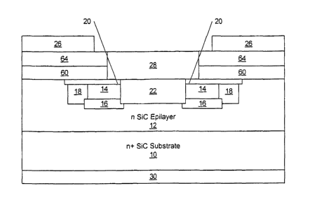
adjustment region 20 and a channel region 60.
CA 02522820 2005-10-19
WO 2004/097926 PCT/US2004/004982
While Figures 2M, 3G and 4E illustrate embodiments of the present invention
as a discrete device, as will be appreciated by those of skill in the art,
Figures 2M, 3G
and 4E may be considered unit cells of a device having multiple cells. Thus,
for
example, additional unit cells may be incorporated into the devices
illustrated in 2M,
3G and 4Eby dividing the devices along their central axis (illustrated as the
vertical
axis in Figures 2M, 3G and 4E) and rotating the divided device about an axis
of the
periphery of the devices illustrated in Figures 2M, 3G and 4E (the vertical
edges of
the devices illustrated in Figures 2M, 3G and 4E). Accordingly, embodiments of
the
present invention include devices such as those illustrated in Figures 2M, 3G
and 4E
as well as devices having a plurality of unit cells incorporating the
implanted regions
illustrated in Figures 2M, 3G and 4E.
While embodiments of the present invention have been described with
reference to particular sequences of operations, as will be appreciated by
those of skill
in the art, certain operations within the sequence may be reordered while
still
benefiting from the teachings of the present invention. For example, in
particular
embodiments of the present invention, the formation of the oxide layer 54' may
be
performed after patterning of the channel epitaxial layer 50'. Accordingly,
the present
invention should not be construed as limited to the exact sequence of
operations
described herein.
Furthermore, embodiments of the present invention have been described with
reference to an n-type SiC layer and p-type silicon carbide well and buried
layers.
However, embodiments of the present invention may also provide complementary
structures with corresponding modifications of the methods of fabrication
described
herein.
As described above, embodiments of the present invention may allow for the
fabrication of very small gate lengths as the gate length is defined by the
etching of
the mask that forms the source region and the well region. Thus, a relatively
low total
on resistance of the resulting SiC MOSFETs may be provided as the MOS channel
resistance may be the dominant resistance in device. Furthermore,
photolithography
steps may be eliminated through the use of the mask thus, potentially,
reducing
processing time and cost compared to a conventional fabrication process.
21
CA 02522820 2005-10-19
WO 2004/097926 PCT/US2004/004982
Furthermore, in embodiments of the present invention incorporating the
epitaxial channel layer, if the gate oxide is formed by thermal oxidation, the
n+ source
regions are not oxidized. Accordingly, the resulting structures may not have
porous,
less reliable oxides that may result from growing oxides on n+ implanted
regions.
Such embodiments may also provide a continuous channel from the n+ source
regions
through the MOS gate regions to the drain area.
In the drawings and specification, there have been disclosed typical preferred
embodiments of the invention and, although specific terms are employed, they
are
used in a generic and descriptive sense only and not for purposes of
limitation, the
scope of the invention being set forth in the following claims.
22