Note: Descriptions are shown in the official language in which they were submitted.
CA 02523166 2005-10-11
-1-
Title: AUDIO SIGNAL DETECTION UTILIZING LOW POWER STANDBY
POWER SUPPLY
Field
[0001] The invention relates to electronic circuitry having a full
operational mode and a low power dissipation standby mode.
Backuround
[0002] Some consumer electronic devices can operate in a full
operation mode and a standby mode. In standby mode, these electronic
devices operate in a non-fully functional state while waiting for an
activation
signal to indicate that the device is to return to full operation mode.
However,
while these devices are in standby mode they can waste significant power.
The wasted power in standby mode can actually account for up to 10% of all
residential power or 20 to 60 W per household in developed countries. This
problem has become a worldwide concern and global energy conscious
agencies such as the International Energy Agency, EPA, Energy Star and EU
have proposed, implemented and/or endorsed energy conscious schemes
such as the Global 1 Watt program. The Global 1 Watt program recommends
that consumer electronic products operating in standby mode should
consume less than 1 W of input power.
[0003] In an attempt to reduce standby power consumption, some
devices may employ a Switched Mode Power Supply (SMPS) that is operated
in burst mode by reducing operating frequency, skipping switching cycles, or
reducing the duty cycle. Regardless of which approach is employed for
implementing burst mode operation, there are several disadvantages. For
instance, when the switching frequency and/or duty cycle of the SMPS is
significantly reduced to reduce power consumption, the transformer in the
SMPS is forced to operate at frequencies for which it is not optimized. This
results in audible noise due to transformer "chatter" or "buzzing". In
addition,
the reduced switching frequency and/or duty cycle produces large ripples in
the output voltage of the SMPS. Accordingly, large filtering capacitors are
typically required when the SMPS operates in burst mode operation.
CA 02523166 2005-10-11
_2_
Furthermore, to implement any of the topologies for burst mode operation, a
more complicated or component intensive control scheme is usually required.
Also, since the same power train is used for both the active and standby
modes, and since the power train is optimized for full power operation, the
power losses do not scale down in the standby mode. Therefore, it is difficult
to achieve low standby power dissipation when the SMPS is operating in burst
mode.
Summary
[0004] In one aspect, at least one embodiment of the invention
provides an electronic device comprising an application circuit; a main power
supply circuit coupled to a power source and the application circuit, the main
power supply circuit operates in a full operation mode and a standby
operation mode, wherein during the full operation mode the main power
supply circuit provides a first power supply signal to the application circuit
and
during the standby mode the main power supply does not provide the first
power supply signal to the application circuit; and, a standby circuit coupled
to
the main power supply circuit, the standby circuit provides a control signal
to
the main power supply circuit to configure the main power supply to operate in
one of the full operation mode and the standby operation mode.
[0005] In some embodiments, the standby circuit can comprise a
standby power supply block that provides a second power supply signal; a
control block coupled to the standby power supply block to receive the second
power supply signal, the control block receives a mode control signal that
indicates the operation mode and generates a coupling signal based on the
mode control signal and determines timing for applying the coupling signal;
and, a coupling unit coupled to the control block and the main power supply
block, the coupling unit generates the control signal based on the coupling
signal.
[0006] In some embodiments, the control block can also receive an
auxiliary control signal and is adapted to override the mode control signal
and
generate the coupling signal based on the auxiliary control signal.
CA 02523166 2005-10-11
-3-
[0007] In another aspect, at least one embodiment of the invention
provides a standby circuit that generates a control signal for configuring a
main power supply circuit to operate in one of a full operation mode and a
standby operation mode. The standby circuit comprises a standby power
supply block comprising a voltage reducer that receives a first supply voltage
and produces a reduced voltage; a transformer having a primary winding and
a secondary winding, the primary winding having first and second nodes, the
first node of the primary winding receiving a switched version of the reduced
voltage, and the secondary winding producing a power supply signal; a
switching stage coupled to the primary winding of the transformer for
providing an oscillation signal to switch the voltage across the primary
winding
based on a switching sequence; and, an oscillation control stage coupled to
the voltage reducer and the switching stage, the oscillation control stage
receives the reduced voltage and produces at least one oscillation control
signal to control the switching of the switching stage, wherein the switching
stage provides the oscillation signal as feedback to the oscillation control
stage for altering the at least one oscillation control signal. The standby
circuit
further comprises a control block coupled to the standby power supply block
to receive the power supply signal, the control block receives a mode control
signal that indicates the operation mode and generates a coupling signal
based on the mode indicated by the mode control signal, the control signal
being based on the coupling signal.
[0008] In some cases, the first node of the primary winding of the
transformer is coupled to the voltage reducer and the switching stage
comprises a first transistor having a collector node, a base node and an
emitter node, and a second transistor having a collector node, a base node
and an emitter node, wherein the emitter nodes of the first and second
transistors are coupled, the collector node of the first transistor is coupled
to
the second node of the primary winding of the transformer, and the collector
node of the second transistor is coupled to the oscillation control stage and
to
ground, and wherein the oscillation control stage provides a first oscillation
CA 02523166 2005-10-11
-4-
control signal to the base node of the first transistor and a second
oscillation
control signal to the base node of the second transistor.
j0009] In some cases, the oscillation control stage comprises a first
resistor having first and second nodes, the first node being coupled to the
output node of the voltage reducer to receive the reduced voltage and the
second node being coupled to the base node of the first transistor for
providing the first oscillation control signal; a capacitor having first and
second
nodes, the first node of the capacitor being coupled to the collector node of
the first transistor and the second node of the capacitor being coupled to the
base node of the second transistor; and, a second resistor having first and
second nodes, the first node of the second resistor being coupled to the
second node of the capacitor and to the base node of the second transistor to
provide the second oscillation control signal, and the second node of the
second resistor being coupled to the collector node of the second transistor
and to ground.
[0010] In some cases, the first node of the primary winding of the
transformer is coupled to the oscillation control stage and the second node of
the primary winding of the transformer is coupled to ground, and the switching
stage comprises a first transistor having a collector node, a base node and an
emitter node, and a second transistor having a collector node, a base node
and an emitter node, wherein the emitter nodes of the first and second
transistors are coupled, the collector node of the first transistor is coupled
to
the output node of the voltage reducer, and the collector node of the second
transistor is coupled to the first node of the primary winding of the
transformer,
and wherein the oscillation control stage provides a first oscillation control
signal to the base node of the first transistor and a second oscillation
control
signal to the base node of the second transistor.
[0011) In some cases, the oscillation control stage comprises a first
resistor having first and second nodes, the first node being coupled to the
base node of the second transistor for providing the second oscillation
control
signal, and the second node being coupled to ground; a second resistor
CA 02523166 2005-10-11
-5-
having first and second nodes, the first node of the second resistor being
coupled to the collector node of the first transistor and to the output node
of
the voltage reducer, and the second node of the second resistor being
coupled to the base node of the first transistor for providing the first
oscillation
control signal; and, a capacitor having first and second nodes, the first node
of
the first capacitor being coupled to the base node of the first transistor and
the
second node of the second resistor, and the second node of the first capacitor
being coupled to the collector node of the second transistor and the first
node
of the primary winding of the transformer.
[0012] The switching frequency of the switching sequence can be
approximately 50 kHz or less.
[0013] In some embodiments, the voltage reducer includes a resistive
portion and a capacitive portion, and the output node of the voltage reducer
is
between the resistive and capacitive portions and provides the reduced
voltage. The capacitive portion can provide voltage filtering.
[0014] The reduced voltage can be approximately 50 Volts.
[0015] In another aspect, at least one embodiment of the invention
provides a standby circuit that generates a control signal for configuring a
main power supply circuit to operate in one of a full operation mode and a
standby operation mode. The standby circuit comprises a standby power
supply block for producing a power supply signal based on a rectified voltage
signal, the standby power supply block including a transformer with a primary
winding and a secondary winding, the primary winding receiving an oscillating
version of the rectified voltage signal, and the secondary winding producing
the power supply signal, the standby power supply block further including an
oscillation block that provides the oscillating version of the rectified
voltage
signal to the primary winding of the transformer, wherein the oscillation
block
uses the oscillation signal as feedback for adjusting the oscillation signal.
The
standby circuit further comprises a control block coupled to the standby power
supply block to receive the power supply signal, the control block receives a
mode control signal that indicates the operation mode and generates a
CA 02523166 2005-10-11
-6-
coupling signal based on the mode indicated by the mode control signal, the
control signal being based on the coupling signal.
[0016) These and other features of the embodiments described herein
are provided in more detail below.
Brief description of the drawincts
[0017) For a better understanding of the various embodiments
described herein and to show more clearly how they may be carried into
effect, reference will now be made, by way of example only, to the
accompanying drawings in which:
Figure 1 is a block diagram of an exemplary embodiment of an
electronic device having a main power supply circuit and a standby circuit;
Figure 2 is a block diagram showing an exemplary embodiment
for the standby circuit of Figure 1; and,
Figure 3 is a block diagram showing another exemplary
embodiment of a standby power supply block that can be used in the standby
circuit of Figure 1.
Detailed descriution
[0018) It will be appreciated that for simplicity and clarity of illustration,
elements shown in the figures have not necessarily been drawn to scale with
respect to one another. Further, where considered appropriate, reference
numerals may be repeated among the figures to indicate corresponding or
analogous elements. In addition, numerous specific details are set forth in
order to provide a thorough understanding of the various exemplary
embodiments. However, it will be understood by those of ordinary skill in the
art that the some of the embodiments may be practiced without these specific
details. In other instances, well-known methods, procedures and components
have not been described in detail so as not to obscure the invention. It
should
further be understood that these exemplary embodiments should not be
construed as limiting the scope of the invention in any way.
CA 02523166 2005-10-11
-7-
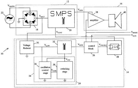
[0019] Referring first to Figure 1, shown therein is an exemplary
embodiment of an electronic device 10 having a main power supply circuit 12,
a standby circuit 14 and an application circuit 16. The electronic device 10
can
generally operate in a full operation mode and a standby operation mode. In
the full operation mode, the main power supply circuit 12 is enabled and
supplies power to the application circuit 16. In the standby operation mode,
the main power supply circuit 12 is inactive and consumes negligible power
(less than 0.5 W in some implementations). However, in standby mode, the
standby circuit 14, which dissipates low power, waits for a mode control
signal
VMOOe to indicate that the mode of operation is to be changed to the full
operation mode. The standby circuit 14 has an efficient design with a minimal
number of components, which results in a reduction in power consumption
and electromagnetic interference. In some implementations, the standby
circuit 14 uses low voltage signals, and hence low voltage semiconductors,
and a simplified transformer design, as is described in more detail below.
[0020] The mode control signal VMOOE can be related to an input signal
that is typically received by the electronic device 10. For instance, in some
embodiments, the electronic device 10 can be an audio amplifier (as is
currently shown) and the mode control signal VMOOe can be an audio input
signal that is provided to the audio amplifier for amplification. In other
embodiments, the application circuit 16 of the electronic device 10 can have a
different structure and function. In some cases, the mode control signal VMO~E
can be another type of electrical signal or an optical or mechanical contact
type signal.
[0021] Since, in some embodiments, the mode control signal Vnnooe is
an input signal that is normally provided to the application circuit 16, it is
provided to both the application circuit 16 and the standby circuit 14. In
this
sense, the standby circuit 14 can automatically enable the main power supply
circuit 12 to power the application circuit 16 when an input signal with
useful
content is provided to the electronic device 10. When the mode control signal
VnnoQe indicates that the mode of operation should change to the full
operation
CA 02523166 2005-10-11
_8_
mode, the standby circuit 14 enables the main power supply sub-circuit 12 by
providing an appropriate value via a power control signal V~oNT. Otherwise,
when the mode of operation is the standby operation mode, the standby
circuit 14 disables the main power supply circuit 12 via the power control
signal VcoNr. The power control signal VcoNT can be applied to the primary
side of the main power supply circuit 12.
[0022] In some embodiments, the electronic device 10 may also
receive an auxiliary control signal VAUx as indicated in Figure 1. The
auxiliary
control signal VAUx, which is optional, can be provided to override the
automatic enabling that is provided by the mode control signal Vnnooe. This is
beneficial for certain circumstances in which the mode control signal VMOOE
includes a noise component and not a valid input signal component. In these
situations, depending on the size of the noise component, the standby circuit
14 may incorrectly activate the main power supply circuit 12. This can be
over-ridden by providing a suitable value via the auxiliary control signal
VAUx.
For instance, the auxiliary control signal VAUx may be configured by a user of
the device 10 to allow automatic triggering by the mode control signal 18 or
the auxiliary control signal VAUx may be configured by a user of the device 10
to not allow automatic enabling by the mode control signal 18. Alternatively,
in
some implementations, the auxiliary control signal VAUx can be directly used
to enable and disable the main power supply circuit 12. For example, the
auxiliary control signal Vaux may be configured by an input device that is
actuated by the user of the electronic device 10. The input device may be
mechanical such as a switch, a button and the like or electronic such as a
transistor that is controlled by other equipment. The auxiliary control signal
Vaux may also be configured by a protection circuit and therefore allow the
electronic device 10 to turn-off in case of a failure.
[0023] In this exemplary embodiment, the main power supply circuit 12
includes a rectifier 18 and a main power supply block 20. The rectifier 18 may
be a full-wave rectifier or any other suitable rectifier. The main power
supply
CA 02523166 2005-10-11
_g_
block 20 may be a switched mode power supply or any other suitable power
supply.
[0024] A power source 22 provides an AC mains voltage VMAiNS to the
main power supply circuit 12. The AC mains voltage VMA~NS is rectified by the
rectifier 18 to produce a rectified AC mains voltage VRECT. The main power
supply block 20 receives the rectified mains voltage VRecT and the power
control signal VcoNT. During full operation mode, the main power supply block
20 is enabled and provides a power supply signal VsuP~ to power the
application circuit 16. During the standby operation mode, the main power
supply block 20 is disabled and does not provide the power supply signal
VSUP1 to the application circuit 16.
[0025] The standby circuit 14 includes a standby power supply block
24, a control block 26 and a coupling unit 28. The standby power supply block
24, the control block 26 and the coupling unit 28 are preferably made from low
power consumption circuits and/or have elegant designs for reducing power
consumption. In some implementations, the standby power supply block 24
can be a low power switched mode power supply. The coupling unit 28
isolates the main power supply circuit 12 from the standby circuit 14. In some
implementations, the coupling unit 28 may be an opto-coupler as currently
shown.
[0026] The standby power supply block 24 receives the rectified AC
mains voltage VRecr and provides a second supply voltage signal VsuP2,
which is used to power the control block 26. The control block 26 monitors the
mode control signal VMOOe and the auxiliary control signal VAUx and, based on
the state of these signals, sends a coupling signal VcouP~e to the coupling
unit
28. If the mode control signal Vnnooe and the auxiliary control signal VAUx
indicate that the mode of operation is the full operation mode, then the
control
block 26 interacts with the coupling unit 28 via the coupling signal VcouP~E
to
generate the power control signal VcoN-r so as to enable the main power
supply 20. Otherwise, the control block 26 interacts with the coupling unit 28
CA 02523166 2005-10-11
-10-
to generate the power control signal VcoNT so as to not enable the main power
supply block 20.
[0027] The standby power supply block 24 includes a voltage reducer
30, a transformer 32, and an oscillation block 34. The oscillation block 34
includes an oscillation control stage 36 and a switching stage 38. The
transformer 32 and the oscillation block 34 are connected in parallel with the
voltage reducer 30. There is also a feedback connection from the switching
stage back 38 back to the oscillation control stage 36.
[0028] The voltage reducer 30 receives the rectified AC mains voltage
VRecr and produces a reduced voltage Vow. In some implementations, the
voltage reducer 30 can also include an auxiliary rectifier and the voltage
reducer 30 can be directly connected to the power source 22 to receive the
voltage V,u,~iNS. The voltage reducer 30 can be a passive or an active
circuit.
Passive circuits that can be used for the voltage reducer 30 include resistive
and/or reactive components and can be in the form of resistive or capacitive
voltage dividers. Active circuits that can be used for the voltage reducer 30
can have a switching component; examples of active circuits include, but are
not limited to, switched mode power supplies and phase-controlled AC
switches such as thyristors.
(0029] The oscillation control stage 36 provides at least one control
signal Vcosc to the switching stage 38 to turn the switching stage 36 on and
off. The number of control signals that are provided to the switching stage 38
can depend on the number of switches that are in the switching stage 38. The
oscillation control stage 36 can be made using passive or active components.
Passive components can include resistive, and reactive components. Active
components can include transistors that provide switching control signals. The
oscillation control stage 36 can be implemented so that the oscillation
control
signal Vcosc is a constant or variable, linear or non-linear voltage or
current
control signal.
[0030] The switching stage 36 includes at least one switch. In some
embodiments, the switching stage 36 can be a two-transistor switch. The
CA 02523166 2005-10-11
-11-
output node of the switching stage 38 is an oscillation signal Vosc that is
provided to the transformer 32 to control the output voltage VsuP2 of the
transformer 32. The switching stage 36 can be in an open or closed state.
When the switching stage 36 is activated and closes, a first voltage is
applied
to the primary of the transformer 32 via the oscillation signal Vosc. When the
switching stage 36 is open, a second voltage is applied to the primary of the
transformer 32. The frequency and duty cycle of the switching stage 38
switches the voltage across the primary of the transformer 32 and hence the
output voltage of the transformer 32. The frequency and duty cycle of the
switching stage 38 depends on the configuration of the oscillation control
stage 36, the values of the components used in the oscillation control stage
36, the parameters of the switching components, the parameters of the
transformer 32 and the topology of the standby power supply block 24.
[0031] The transformer 32 also provides isolation between the standby
power supply block 24 and the remainder of the standby circuit 14. Due to
very low output power required to power the control block 28 and the use of
the voltage reducer 30, feedback from the transformer 32, an auxiliary supply
or voltage clamping windings do not have to be used. The use of the voltage
reducer 30 also makes the design less sensitive to the effects of the leakage
inductance in terms of peak voltages, output voltage regulation and switching
power losses. In some implementations, the transformer 32 can have a
simplified design with one primary winding and one secondary winding. Also,
in some implementations, a small UU core with sectional bobbin can be used
for the transformer 32, which reduces the cost and allows the design to meet
EMI and safety requirements. The output voltage VsuP2 of the transformer 32
is used to supply power to the components of the control block 26. The output
voltage VsuP2 depends on the voltage signal V~oW, the frequency and duty
cycle for which the switching stage 38 is in the opened and closed stages, the
characteristics of the primary and secondary windings such as the number of
turns used and the coupling, and the components that are on the secondary
side of the transformer 32.
CA 02523166 2005-10-11
-12-
[0032] Component values can be chosen for the oscillation control
stage 36, the switching stage 38, and the transformer 32 so that the standby
power supply block 24 acts as a low-power switched mode power supply. In
some implementations, the structure of the control block 26 and the way in
which the control block 26 is connected to the transformer 32 can be selected
so that the standby power supply block 24 acts as a forward or flyback
switched mode power supply. Further, these blocks can be configured, and
the values of components in these blocks can be selected, so that the standby
power supply block 24 operates in a discontinuous, critically discontinuous or
continuous mode which all refer to the current through the whole transformer
32. Discontinuous mode is advantageous because of low power
requirements, which allows for smaller transformer size, lower turn-ON
switching losses and improved EMI.
[0033] The application circuit 16 can be any electronic circuit that
requires supply power. In some embodiments, the application circuit 16 is an
audio amplifier and includes an amplification circuit 40 and a speaker 42.
Accordingly, in these embodiments, an input audio signal can be provided as
the mode control signal Vnno~E and the presence of audio triggers the control
block 26 to enable the main power supply circuit 12. When the main power
supply circuit 12 is enabled, power is supplied to the amplification circuit
40
which also receives the input audio signal and produces an amplified audio
signal that is output by the speaker 42. When there is no audio signal, the
main power supply circuit 12 is put into standby operation mode so that it
does not consume any power.
[0034] The voltage reducer 30 allows low voltage components to be
used in the oscillation block 34, and a simplified design for the transformer
32.
For instance, the coupling requirement for the transformer 32 can be reduced
which results in lower EMI, and eases the safety requirements for the standby
power supply block 24. In conventional switched mode power supplies, higher
voltages are used which requires the use of higher voltage components, and
more complex control schemes and designs for the transformer.
CA 02523166 2005-10-11
-13-
[0035] Furthermore, the voltage reducer 30, and the low power
requirements allow lower switching frequencies to be used without increasing
the size of the transformer 32. For example, switching frequencies of
approximately 50 kHz or less can be used. This is advantageous since the
third harmonic will be at or lower than the 150 kHz limit for Electromagnetic
Interference (EMI). In addition, feedback is provided from the switching stage
38 to the oscillation control stage 36 rather than relying on feedback from
the
transformer 32. In conventional switched mode power supplies, the
transformer has additional windings to provide feedback for oscillation which
results in a more complicated design.
[0036] The voltage reducer 30 also allows for a reduction in circuit
complexity for other components in the standby power supply block 24. For
instance, the voltages Vow and Vosc can be directly connected to the
oscillation block 34. All of these simplifications allow the design for the
standby power supply block 24 to be very compact.
[0037] Referring now to Figure 2, shown therein is an exemplary
embodiment 14' for the standby circuit of Figure 1. A list of exemplary values
for the components shown in Figure 2 is provided in Table 1. The standby
circuit 14' includes a standby power supply block 24', a control block 26' and
the coupling unit 28'. The standby power supply block 24' includes a voltage
reducer 30', a transformer 32', and an oscillation control block 34' having an
oscillation control stage 34' and a switching stage 38'. In this exemplary
implementation, the standby power supply block 24' has a flyback topology.
The control block 26' includes a regulator 44, a detection circuit 46 and a
control circuit 48.
[0038] The voltage reducer 30' can be a resistor-capacitor circuit with a
resistive portion that includes resistors R1 and R2 connected in series and a
capacitive portion that includes a capacitor C1. A first node of the resistor
R1
is connected to the rectified AC mains voltage VRECr and a second node of
the resistor R1 is connected to a first node the resistor R2. A second node of
the resistor R2 is then connected to a first node of the capacitor C1. The
CA 02523166 2005-10-11
-14-
second node of the capacitor C1 is connected to ground. The output voltage
Vow is taken from the node between the resistor R2 and the capacitor C1.
The values of the resistors R1 and R2 are selected to provide a sufficient
reduction in the magnitude of the voltage VRECT to allow low voltage
components to be used in the standby circuit 24'. In some implementations,
these parameters are selected to obtain a voltage reduction of about 1/3,
which results in a maximum voltage of about 50 Volts. The use of the
capacitor C1 in the voltage reducer 30' provides some filtering to smooth the
output voltage Vow.
[0039] In some implementations, the voltage reducer 30' can include
an auxiliary rectifier that can be connected in series with the resistors R1
and
R2 to provide a reduced rectified voltage to the capacitor C1. In this case,
the
resistors R1 and R2 are connected to a power source to receive the voltage
VMAINS. In other implementations, instead of using the resistors R1 and R2, a
capacitor can be used to reduce power consumption (i.e. the power
dissipation of resistors R1 and R2).
[0040] The oscillation control stage 36' includes two resistors R3 and
R4 and a capacitor C2. The switching stage 38' includes an npn bipolar
junction transistor Q1 and a pnp bipolar junction transistor Q2 connected in
series such that the emitter of transistor Q1 is connected to the emitter of
transistor Q2. The two transistors Q1 and Q2 can be low voltage transistors
because of the voltage reduction provided by the voltage reducer 30'. The two
transistors Q1 and Q2 receive two control signals Vcosc~ and Vcosc2 but act
as a single switch to modulate the voltage across the primary of the
transformer 32'. The voltage differential between the control signals Vcosc~
and Vcoscz determine whether the transistors Q1 and Q2 are on or off. For
both transistors Q1 and Q2 to be conducting, feedback is used by the
oscillation control stage 36' as described below. The use of the two
transistors
Q1 and Q2 allows the oscillation control stage 36' to have a more simplified
design and also avoids the use of extra windings on the transformer 32'.
CA 02523166 2005-10-11
-15-
[0041] A first node of resistor R3 is connected to the output node of the
voltage reducer 30' and a first node of the primary winding of the transformer
32'. A second node of the resistor R3 is connected to the base node of the
transistor Q1 to bias the transistor Q1. The collector node of the transistor
Q1
is connected to a second node of the primary winding of the transformer 32'.
Accordingly, the voltage Vow is provided to the transformer 32' and a
switched version of the voltage Vow is provided to the switching stage 38',
depending on whether the switching stage 38' is ON (i.e. conducting) or OFF
(i.e. not conducting). A first node of the capacitor C2 is connected to both
the
collector node of the transistor Q1 and the second node of the primary
winding of the transformer 32'. A second node of the capacitor C2 is
connected to the base node of the transistor Q2. A first node of the resistor
R4 is connected to the base node of the transistor Q2 and the second node of
the capacitor C2. A second node of the resistor R4 is also connected to
collector node of the transistor Q2 and to ground.
[0042] At the beginning of a switching cycle, both of the transistors Q1
and Q2 are off. The voltage Vow is at the first node of the primary winding of
the transformer 32'. The capacitor C2 is charged and at first appears as an
open circuit. Accordingly, the voltage Vow is at the second node on the
primary winding of the transformer 32'. Current then begins to flow through
the resistor R3, from the base node to the emitter node of the transistor Q1,
from the emitter node to the base node of the transistor Q2, and the resistor
R4. This causes the transistors Q1 and Q2 to turn on. When both of the
transistors Q1 and Q2 turn on, they appear as small resistors and provide a
low resistance path to ground. The capacitor C2 then begins to discharge
along the path defined from the collector node to the emitter node of
transistor
Q1, the emitter node to the collector node of transistor Q2 to ground and then
through the resistor R4. The capacitor C2 also discharges through the path
defined from the collector node to the emitter node of transistor Q1, and the
emitter node to the base node of transistor Q2.
CA 02523166 2005-10-11
-16-
[0043] As the current through the transistors Q1 and Q2 increases and
the capacitor C2 discharges, a threshold point is reached at which point the
transistors Q1 and Q2 are no longer in saturation. The voltage (i.e. Yosc)
across the transistors Q1 and Q2 rises, the capacitor C2 starts to charge
through the resistor R4, which increases the control voltage Vcoscz which in
turns causes transistors Q1 and Q2 to turn off. During this turn-off
transition,
the portion of the oscillation control stage 36' defined by the capacitor C2
and
the resistor R4 provides positive feedback in order to more quickly turn off
the
switching stage 38'. When both transistors Q1 and Q2 turn off, the capacitor
C2 charges to Vow plus the voltage across the primary winding of the
transformer 32'. As the capacitor C2 charges, the control voltage Vcoscz
starts to drop. When the control voltage Vcoscz becomes lower than a certain
turn-on threshold voltage, current starts to flow through the resistor R3,
from
the base node to the emitter node of the transistor Q1, from the emitter node
to the base node of the transistor Q2 and the resistor R4. The voltage Vosc
then starts to drop and the cycle repeats. The rate at which the capacitor C2
charges and discharges is dictated by the RC time constant determined by
the capacitor CZ, the resistor R4 as well as the parameters of the transistors
Q1 and Q2. The switch timing or switching sequence defined by the turn-ON
and turn-OFF times of the transistors Q1 and Q2, can be adjusted by varying
the values of the components C2, R3 and R4 so that the standby circuit 24'
operates in discontinuous, critically discontinuous or continuous mode for a
specific load.
[0044] As the switching stage 38' is turning on and off, and the
capacitor C2 is charging and discharging, the voltage across the primary
winding of the transformer 32' is being switched. This switching voltage is
then transferred to the secondary winding of the transformer 32' and is
provided as VsuPZ to power the control block 26'. Accordingly, the voltage
VsuPZ is provided to the control block 26' during both the ON and OFF periods
of the switching sequence of the switching stage 38'.
CA 02523166 2005-10-11
-17-
[0045] The regulator 44 receives the AC signal VSUP2 and produces a
constant voltage Vcc, which powers the signal detection circuit 46 and the
control circuit 48. In this exemplary embodiment, the regulator 44 includes a
diode D1, capacitors C3 and C4, and a zener diode Z1. A first node of the
diode D1 is connected to a first node of secondary winding of the transformer
32'. A second node of the diode D1 is connected to a first node of the
capacitor C3, a first node of the zener diode Z1 and to a secondary ground.
The second node of the capacitor C3 and the second node of the zener diode
Z1 are connected to a first node of the capacitor C4 and to a second node of
the secondary winding of the transformer 32'. The second node of the
capacitor C4 is connected to secondary ground. The output Vcc of the
regulator 44 is taken from the node between the capacitors C3 and C4.
[0046] The diode D1 acts as a reverse-biased, half-wave rectifier to
produce a half wave rectified signal that is smoothed out by the capacitors C3
and C4. The smoothed out signal is clamped by the zener diode Z1 to
produce a regulated voltage Vcc that is similar to the breakdown voltage of
the zener diode Z1. The regulated voltage Vcc is fed to the signal detection
circuit 46 and the control circuit 48 to power these circuits.
[0047] The control block 26' includes a voltage conversion stage 50
that can be used to further modify the regulated voltage Vcc to provide a
voltage reference VReF. The voltage reference VReF is used by various
components in the signal detection circuit 46 and the control circuit 48 for
performing comparisons and the like. In this exemplary embodiment, the
voltage conversion stage includes a resistor R5, and a zener diode Z2. A first
node of the resistor R5 is connected to the output node of the regulator 44.
The second node of the resistor R5 is connected to the cathode of the zener
diode Z2. The anode of the zener diode Z2 is connected to the secondary
ground. The voltage VReF IS taken from the cathode of the zener diode Z2.
Accordingly, the voltage VREF is set to the breakdown voltage of the zener
diode Z2.
CA 02523166 2005-10-11
-18-
[0048] The signal detection circuit 46 monitors the mode control signal
VMODE to determine if the standby circuit 14' should enable the main power
supply circuit 12. In some implementations, the mode control signal VMOO~ can
be an input audio signal and when the signal detection circuit 46 detects that
the input audio signal reaches a specified minimum voltage, then the signal
detection circuit 46 indicates this detection via detection signal V~eT. The
control circuit 48 receives the detection signal VoET and based on the
information in this signal, enables or disables the main power supply block 20
via the signal VcoNT.
[0049] In this exemplary embodiment, the signal detection circuit 46
includes an amplification stage 52, a filtering stage 54, a comparator stage
56
and an output stage 58. Structures which are suitable for these stages include
circuit topologies with components such that the stages dissipate low power
and can accommodate signals having the frequency and amplitude
characteristics of the mode control signal Vnnooe.
[0050] The amplification stage 52 can be any suitable amplifier that
receives the mode control signal VMO~E and amplifies this signal. In this
exemplary implementation, the amplification stage 52 includes resistors R6,
R7 and R8, zener diode Z3, capacitor C5 and operational amplifier U1.
Resistors R6 and R7 act as a voltage divider to center the output node of the
operational amplifier U1 about a voltage that is in between the reference
voltage VREF and secondary ground. A first node of resistor R6 is connected to
the reference voltage VReF and a second node of the resistor R6 is connected
to a first node of the resistor R7 and to the non-inverting input node of the
operation amplifier U1. The second node of the resistor R7 is connected to
secondary ground. The cathode of the zener diode Z3 is connected to the
non-inverting input node of the operational amplifier U1. The anode of the
zener diode Z3 is connected to secondary ground. Resistor R8 and capacitor
C5 are connected in parallel across the output node and the inverting input
node of the operational amplifier U1. The mode control signal Vnno~E is
connected to the inverting input node of the operational amplifier U1. The
CA 02523166 2005-10-11
- 19-
mode control signal Vnnooe is amplified to an appropriate level for further
processing by the other components of the signal detection circuit 46.
[0051] The amplified signal is then filtered by the filtering stage 54
which is any suitable high-pass filter with a low cutoff frequency for
removing
any DC and very low frequency components in the amplified signal. In this
exemplary implementation, the filtering stage 54 includes a capacitor C6 and
a resistor R9 in a high-pass configuration. A first node of the capacitor C6
is
connected to the output node of the operational amplifier U1, and a second
node of the capacitor C6 is connected to a first node of the resistor R9. The
other node of the resistor R9 is connected to secondary ground.
[0052] In the comparator stage 56, the filtered signal is compared with
a first comparison voltage to determine if the filtered signal includes noise
or a
signal component. This determination is reflected in the output signal of the
comparator stage 56 that is provided to the output stage 58. In this exemplary
implementation, the comparator stage 56 includes two resistors R10 and R11
and an operational amplifier U2. A first node of the resistor R10 is connected
to the reference voltage signal VReF and a second node of the resistor R10 is
connected to a first node of the resistor R11 and to the non-inverting input
node of the operational amplifier U2. A second node of the resistor R11 is
connected to secondary ground. The output node of the filtering stage 54 is
connected to the inverting input node of the operational amplifier U2 for
comparison with the first comparison voltage. The first comparison voltage is
determined by the reference voltage VReF and the voltage divider provided by
the resistors R10 and R11. When the amplitude of the filtered signal is
greater
than the first comparison voltage, then the output of the operational
amplifier
U2 is pulled down to the negative supply voltage of the operational amplifier
U2, which in this implementation is secondary ground. When the amplitude of
the filtered signal is less than the first comparison voltage, then the output
of
the operational amplifier U2 is pulled up to the positive supply voltage of
the
operational amplifier U2, which is Vcc.
CA 02523166 2005-10-11
-20-
[0053] The output stage 58 includes resistors R12, R13 and R14, a
capacitor C8, a transistor Q5 and a diode D6. A first node of the resistor R12
is connected to the reference voltage VREF, and a second node of the resistor
R12 is connected to both the base node of the transistor Q5 and a first node
of the resistor R14. A second node of the resistor R14 is connected to
secondary ground. The two resistors R12 and R14 act as a voltage divider to
provide a constant voltage to the base node of the transistor Q5 that is a
fraction of the reference voltage VReF. A first node of the resistor R13 is
connected to the reference voltage VREF, and a second node of the resistor
R13 is connected to the anode of the diode D6 and the first node of the
capacitor C8. A second node of the capacitor C8 is connected to secondary
ground. The second node of the resistor R13 provides the output signal Voer
of the signal detection circuit 46. The cathode of the diode D6 is connected
to
the collector node of the transistor Q5. The emitter node of the transistor Q5
is
connected to the output node of the operational amplifier U2 (i.e. the output
of
the comparator stage 56). The transistor Q5 acts as a switch and the diode
D6 ensures low leakage current to the STANDBY ON control signal.
[0054] If the mode control signal VMO~E includes a signal indicating that
the mode of operation should be full operation mode, then the output of the
comparator stage 56 will be pulled to ground. The emitter node of the
transistor Q5 will be at a lower voltage than the base node of the transistor
Q5
such that the transistor Q5 will turn on. This will then pull the output
voltage
VpET of the output stage 58 to a low voltage determined by the diode D6, the
saturation voltage of the transistor Q5 and the output-low voltage of the
operational amplifier U2. Otherwise, if the mode control signal Vnnooe does
not
include a signal indicating that the mode of operation should be full
operation
mode, then the output of the comparator stage 56 will be Vc~. The transistor
Q5 will be off and the current flowing through the resistor R13 will start to
charge the capacitor C8. The output VpET of the output stage 58 will then be
linearly rising to the reference voltage VREF. In audio circuits there are
inherit
pauses in audio signals. Accordingly, when the mode control signal VMO~E is
an audio signal, the capacitor C8 provides a delay for switching into the
CA 02523166 2005-10-11
-21 -
standby mode of operation; i.e. the configuration of the output stage 58 along
with the capacitor C8 ensures that short pauses in the audio signal used for
the mode control signal VMOOe will not cause the main power supply circuit 12
to switch to the standby mode of operation. Accordingly, the portion of the
circuit including the capacitor C8 determines the timing for applying the
coupling signal VcouP~e and hence the control signal VcoNT.
[0055] The control circuit 48 includes two paths with the first path
having a first comparator stage 60 and a first output stage 62 and the second
path having a second comparator stage 64, a feedback stage 66 and a
second output stage 68. The comparator stages 60 and 64 work in a
complementary manner to one another. The first comparator stage 60 and the
first output stage 62 drive the coupling unit 28 to provide the VCONT signal
to
the main power supply circuit 12. The second comparator stage 64 and the
feedback stage 66 provide feedback to prevent the switch Q5 in the output
stage 58 of the signal detection circuit 46 from turning back on in certain
conditions. This feedback loop is required to ensure turn-off when the main
power supply circuit 12 is turning off to a standby operation mode.
[0056] The first comparator stage 60 includes resistors R15, R16 and
R17, and operational amplifier U3. A first node of the resistor R15 is
connected to the reference voltage VREF, and a second node of the resistor
R15 is connected to a first node of the resistor R16 and to the non-inverting
input node of the operational amplifier U3. A second node of the resistor R16
is connected to secondary ground. The resistor R17 is connected between the
output node and positive input node of the operational amplifier U3 and
provides positive feedback and hysteresis. The inverting input node of the
operational amplifier U3 is connected to the output node of the signal
detection circuit 46 to receive the voltage VoeT.
(0057] The first comparator stage 60 compares VDET to a second
comparison voltage. The second comparison voltage is determined by the
reference voltage VREF, and the voltage divider provided by the resistors R15
and R16. When the detection signal Veer is greater than the second
CA 02523166 2005-10-11
-22-
comparison voltage, the output of the operational amplifier U3 goes to the
negative supply voltage, which in this case is secondary ground. When the
detection signal VoET is lower than the second comparison voltage, the output
of the operational amplifier U3 goes to the positive supply voltage, which in
this case is Vcc.
[0058] The output stage 62 includes a transistor Q3, and a diode D3.
The anode of the diode D3 is connected to a supply voltage VS and the
cathode of the diode D3 is connected to the collector of the transistor Q3. In
some implementations, the supply voltage VS is 15 V and is supplied by the
main power supply circuit when it is operating in full operation mode. The
base node of the transistor Q3 is connected to the output node of the
operational amplifier U3. The emitter node of the transistor Q3 is connected
to
a first input node of the coupling unit 28 and the output node of the
operational amplifier U3 is connected to a second input node of the coupling
unit 28. The transistor Q3 is used as a switch and the diode D3 biases the
transistor Q3 so that it acts as a true switch. As indicated, an optional LED
can be connected to the emitter of the transistor Q3 to receive the LED signal
LED1 to show when the electronic device is operating in stand-by mode.
[0059] With regards to the coupling unit 28, in some implementations
the coupling unit 28 is an opto-coupler that, for simplifying the description,
includes a photo-diode PD and a photo-transistor PT. A first node of the
photo-transistor PT is connected to a first output node of the coupling unit
28
and provides the control signal VcoNT. A second node of the photo-transistor
PT is connected to a second output node of the coupling unit 28 and is
connected to ground. The first input node of the coupling unit 28 is connected
to the anode of the photo-diode PD and the second input node of the coupling
unit 28 is connected to the cathode of the photo-diode PD.
[0060] When the mode control signal VMOpE indicates that the mode of
operation should be full operation mode, the output of the operational
amplifier U3 will be high (i.e. at the potential of Vcc). The transistor Q3
will be
on and there will be a reversed differential voltage across the photo-diode
PD.
CA 02523166 2005-10-11
-23-
In this case, light is not produced by the photo-diode PD and the output of
the
photo-transistor PT is open, and hence the control signal VcoNT will be high.
The main power supply block 20 includes structure such that it is enabled
when the signal VcoNT is high.
[0061] When the mode control signal VMO~e indicates that the mode of
operation should be standby operation mode, the output of the operational
amplifier U3 will be low (i.e. at the secondary ground). The transistor Q3
will
be off and the photo-diode PD will be on. In this case, light is produced by
the
photo-diode PD and the output of the photo-transistor PT, and the signal
V~oN-r, will be low. The main power supply block 20 will be disabled when the
signal VcoNr is low.
[0062] The transistor Q3 is connected to the voltage Vs through the
diode D3. Using an external voltage supply allows the brightness of an LED
connected to signal LED1 to be increased during the full operation mode
without increasing the power consumption of the standby circuit 14'. The LED
that is used can be a bicolor LED and can be connected between the nodes
providing the signals LED1 and LED2 to indicate when the electronic device
10 is operating in full operation mode and standby operation mode. The LED2
signal is also used to supply power to the coupling unit 28 when the signal
VcouP~E is low. The signal LED1 can be referred to as a first indication
signal
and the signal LED2 can be referred to as a second indication signal.
[0063] The LED1 and LED2 signals are not limited for use only in LED
applications. The LED1 and LED2 signals can also be used to control
external electronic circuits. For example, the LED1 and LED2 signals can be
used also to mute the amplifier 38 during ON/OFF transitions, control the
sleep/wake-up transitions for a microcontroller, control a 12V trigger output
(a
12V trigger output is common in Hi-Fi audio systems), and the like.
[0064] The second comparator stage 64 includes an operational
amplifier U4 and uses the second comparison voltage provided by the voltage
divider formed by the resistors R15 and R16, and the detection signal VoEr.
The second comparison voltage is connected to the inverting input node of
CA 02523166 2005-10-11
-24-
the operational amplifier U4 and the detection signal VoEr is connected to the
non-inverting input node of the operational amplifier U4. Accordingly, when
the signal VneT is low, which indicates that the mode control signal Vnnooe is
signifying that the mode of operation should be full operation mode, the
output
of the operational amplifier U4 will go to the negative supply voltage which
in
this case is secondary ground. When the signal VoET is high, which indicates
that the mode control signal Vnnooe is signifying that the mode of operation
should be standby operation mode, the output of the operational amplifier U4
will go to the positive supply voltage, which in this case is Vcc.
Accordingly,
the second comparator stage 64 produces the opposite result that is produced
by the first comparator stage 60.
[0065] The feedback stage 66 includes resistors R18, R19 and R20,
capacitor C7, diode D5, and transistor Q4. The anode of the diode D5 is
connected to the output node of the operational amplifier U4, and the cathode
of the diode D5 is connected to a first node of both the resistor R19 and the
resistor R20. A second node of the resistor R20 is connected to secondary
ground. A second node of the resistor R19 is connected to a first node of the
capacitor C7. A second node of the capacitor C7 is connected to the base
node of the transistor Q4 and a first node of the resistor R18. A second node
of the resistor R18 is connected to secondary ground. The emitter node of the
transistor Q4 is also connected to secondary ground, and the collector node
of the transistor Q4 is connected to the base node of the transistor Q5 of the
output stage 58 of the signal detection circuit 46.
[0066] When the output of the second comparator stage 64 is Vcc, this
signifies that V~eT is greater than the reference voltage VREF which means
that
the mode control signal Vnno~e indicates that the mode of operation should be
the standby mode. In this case, when the feedback stage 66 activates, the
output voltage of the operational amplifier U4 charges the capacitor C7
supplying a current to the base node of the transistor Q4 to turn on the
transistor Q4. When the transistor Q4 turns on, it pulls the base node of the
transistor Q5 to secondary ground which ensures that the transistor Q5
CA 02523166 2005-10-11
-25-
remains off. This ensures that there is no false switching between modes
when there is some noise in the mode control signal VnnooE. The noise can be
voltage transients caused by the turning-off of the main power supply circuit
12. The resistor R19 and the capacitor C7 provide a time constant for the
pulse generated at the output of the transistor Q4. The resistor R20 provides
a discharge path for the capacitor C7.
[0067] The output stage 68 includes resistors R21 and R22, and diode
D4. The cathode of the diode D4 is connected to the output node of the
operational amplifier U4 and the anode of the diode D4 is connected to a first
node of the resistor R22. The second node of the resistor R22 is connected to
a first node of the resistor R21. The second node of the resistor R21 is
connected to the cathode of the diode D4 and the output node of the
operational amplifier U4. As indicated, an optional LED can be connected to
the first node of the resistor R21. The resistors R21, and R22 and the diode
D4 are used to control the intensity of the signal LED2 during both the full
operation and standby modes of the electronic device 10. The diode D4 also
reduces the power consumption of the standby circuit 14' during standby
operation mode (i.e. the output of the amplifier U4 is high, which in this
exemplary case is Vcc). The use of a bicolor LED allows the output stage 68
to be connected to the coupling unit 28 to provide supply power to the
coupling unit 28 when the signal VcouP~e is low. If a bicolor LED is not used,
then another suitable electronic component can be used to connected the
LED2 signal to the coupling unit 28 to provide supply power when needed.
For instance, a diode can be connected between the LED2 and LED1 signal
outputs to provide the required power for the coupling unit 28 if a bicolor
LED
is not used. In this case, the cathode of the diode is connected at the node
marked LED1.
[0068] The control circuit 48 can also include two additional external
auxiliary inputs STANDBY ON and STANDBY OFF. The STANDBY ON
signal is connected to the output node of the signal detection circuit 46. The
STANDBY OFF signal is connected to the non-inverting input node of the
CA 02523166 2005-10-11
-26-
operational amplifier U3 in the first comparator stage 60. These two external
control signals can be used to override the automatic operation of the standby
circuit 14' to turn the main power supply block 20 on or off. When the
STANDBY ON signal is set to ground, this provides the same effect as when
the signal VpET is low and which ultimately enables the main power supply
circuit 12 to operate in the full operation mode. When the STANDBY OFF
signal is set to ground, this provides the same effect when the signal VpEr is
high and ultimately enables the main power supply circuit 12 to operate in the
standby operation mode. Further, when the VoeT signal is low due to the
presence of a valid input signal component in the mode control signal Vnno~e,
the signal VpeT is approximately 1V. If the STANDBY OFF signal is brought
to a lower level than the VoeT signal, then the electronic device 10 can be
placed into standby operation mode. The auxiliary input STANDBY OFF can
override the delay associated with the capacitor C8.
20
CA 02523166 2005-10-11
-27-
TABLE 1. EXEMPLARY VALUES FOR COMPONENTS IN FIGURE 2
~_~p ~ uC~~,p,.~~'~ ~2,~~~~~~~ ~
a, ~t ~ IC 'i sW ~~L. ~~i Pt'
F~~~;"-~yh: n~ rf kI- ~fxi ~_
~~
C1 Ca acitor .OlUF 100V 10%
C2 C 470PF 100V 5%
a acitor
C3 _ 100PF 100V 5%
_
Ca acitor
C4 Ca acitor 1UF 50V 10%
C5 Ca acitor 100PF 50V 5%
C6 Ca acitor .1UF 50V 5%
D1 Diode BAS16
D3 Diode BAS16
D4 Diode BAS16
D5 Diode BAS16
D6 Diode BAS16
Q1 Transistor MMBT5551
2 Transistor MMBT5401
3 Transistor MMBT4401
4 Transistor MMBT4401
Transistor MMTB4401
R01 Resistor 100K 1/4W 1%
R02 Resistor 475K 1/4W 1%
R03 Resistor 1M00 1/8W 1%
R04 Resistor 1M00 1/8W 1%
R05 Resistor 10K0 1/8W 1%
R06 Resistor 499K 1/8W 1%
R07 Resistor 499K 1/8W 1%
R08 Resistor 499K 1/8W 1%
R09 Resistor 100K 1/8W 1%
R10 Resistor 499K 1/8W 1%
R11 Resistor 1K00 1/8W 1%
R12 Resistor 255K 1/8W 1%
R13 Resistor 2M21 1/8W 1%
R14 Resistor 499K 1/8W 1%
R15 Resistor 220K 1/8W 5%
R16 Resistor 499K 1/8W 1%
R17 Resistor 4M7 1/8W 5%
R18 Resistor 100K 1/8W 1%
R19 Resistor 255K 1/8W 1%
R20 Resistor 499K 1/8W 1%
R21 Resistor 4.02K 1/8W 1%
R22 Resistor 1K 1/8W 1%
Z1 Zener Diode MMBZ5237 8.2V
Z2 Zener Diode MMBZ5234 6.2V
Z3 Zener Diode MMBZ2283.9V
32 Transformer ~8 mH
CA 02523166 2005-10-11
-28-
[0069] Referring now to Figure 3, shown therein is a block diagram of
another exemplary embodiment of a standby power supply block 24" that can
be used in the standby circuit 14. The standby power supply block 24"
includes the voltage reducer 30', a transformer 32", and an oscillation block
34" having an oscillation control stage 36" and a switching stage 38". The
switching stage 38" includes the two transistors Q1 and Q2 connected such
that the collector node of the transistor Q1 is connected to the output node
of
the voltage reducer 30' (i.e. the node between the resistor R2 and the
capacitor C1). The emitter node of the transistor Q1 is connected to the
emitter node of the transistor Q2. The oscillation control stage 36" includes
resistors R3 and R4 and capacitor C2. A first node of the resistor R3 is
connected to the base node of the transistor Q2 and a second node of the
resistor R3 is connected to ground. A first node of the resistor R4 is
connected to the collector node of the transistor Q1 and the output node of
the voltage reducer 30'. A second node of the resistor R4 is connected to the
base node of the transistor Q1. A first node of the capacitor C2 is connected
to the second node of the resistor R4 and the base node of the transistor Q1.
A second node of the capacitor C2 is connected to the collector node of the
transistor Q2 and to a first node of the primary winding of the transformer
32".
A second node of the primary winding of the transformer 32" is connected to
ground.
[0070] The oscillation block 24" operates in a similar fashion as the
oscillation block 24' since the switching arrangement, i.e. components R3, R4,
C2, Q1 and Q2, have not changed. Rather, the topology of the switching
arrangement of the oscillation block 24" is a somewhat mirrored version of the
switching arrangement of the oscillation block 24'. Accordingly, the operation
of the standby power supply block 24 does not need to be discussed. Further,
the component values for the standby power supply block 24" are similar to
those given in Table 1.
[0071] With respect to the standby power supply block 24', it is to be
noted that the second node of the resistor R3 can be connected to a different
CA 02523166 2005-10-11
-29-
reference voltage potential. However, this node can only be connected to a
"high" reference voltage potential during the OFF state of the switching stage
38'. The same is generally true for the standby power supply block 24" taking
into account the mirrored configuration and so the "high" reference voltage
becomes low and so on and so forth.
[0072] Further, with respect to both standby power supply blocks 24',
and 24", the signal Vcosc~ can be variable, for example it can be linearly
changing. In addition, the signal Vcosc~ can be provided by an RC circuit or
another type of suitable circuit. Further, reversing the polarity of the power
supply (i.e. the voltage Vow becomes negative referenced to ground) will
require implementing the transistor Q1 with a pnp transistor and transistor Q2
with an npn transistor.
[0073] With regards to both oscillation blocks 34' and 34", it is to be
noted that transistors Q1 and Q2 are not limited to bipolar transistors.
Further,
in some implementations a single 4 pin integrated switching device can be
used that provides the functionality of transistors Q1 and Q2.
[0074] It should be understood that various modifications can be made
to the embodiments described and illustrated herein without departing from
the invention, the scope of which is defined in the appended claims.