Note: Descriptions are shown in the official language in which they were submitted.
CA 02523264 1995-12-05
wo 9sris~os' FCTlUS95I15733 ' .
z
PhASMA PROC SSOR FOR L G~ WORKPIECES
Field of Invention
The present invention .relates generally ,to
processors for treating workpieces in a vacuum chamber
with'a plasma and more particularly tn~such a proGessQr.
S having plural individually supported dielectric windows
. for.eaupliag an r.f: field originating outside of the
chamber into the chamber to excite the plasma, and/or a
coil for inductively d~riviag the field, wherein the coil
has plural segments . with the same electrical. ' length, each
1D ~includizlg an element connected in parallel with an
element of another segment.
Ha kid Art
Various structures have been daveloped~to supply
r.f. ~.ields from devices outside of a vacuum chataber to.
15 excite a gas in the chamber to a plasma state. The r.f_
fields have been derived from electric field sources
including capacitive electrodes, electromagnetic field
sources including electron ~cyclotran resonators and
induction.,.i_e. maguetic,;field sources including coils.
20 The excited plasma interacts with the workpiece to etch
the workpiece or deposit materials on it. Typically, the
workpiece is. a semiconductor wafer having a , ~larlar
circular surface.
A processor for treating workpieces with an
25 inductively coupled planar plasma (ICP)~is disclosed,
inter a.Iia, by O~x~.e, U.S. Patent x,948,458, commonly
assigned with the present invent3on_ The magnetic field
CA 02523264 1995-12-05
- WO 961,820$. . PGT/US951J.5753
2
is derived from a plazxar coil positioned ,on or adjacent
1a single planar dielectric window that extends in 'a
direction 'generally parallel to the workpiece planar
,surface. Tn commercial devices the window is' usually - ,
' S quartz because this material has low impurity content and
provides optimum results for r.f, field coupling. The
coil is connected to be responsive to an r.f_ source
having a ' frequency in the x~aage of 1 to 100 MHz and
Coupled to the coil by an impedance matching network
including a circuit resonant to the frequency of the
. source. The coil. is disclosed as a planar spiral. having.
external - and internal' terminals connected to be
responsive to the r.f. source. The circular spiral coil
disclosed by Ogle has been modified to include linear,
I5 , elongated elements generally in a spiral configuration,
to process woxl~pieces having square and rectangwlar
shapes.. Caultas et al., U.s. Patent 5,304,279 discloses
a similar device employing permanent magnets in
combination with the planar spiral coil.
Cuomo et al.,' V:S. Patent 5,280,154 and Ogle, U.S.
Patent 5,77,751 disclose a variation. of the
aforementioned processor wherein the lihear spiral coil
is replaced by a solenoidal coil. The solenoidal coil is
wound on a dielectric mandrel or the like and includes
plural helical-like turris, a portion of which extend
along the dielectric w~.nr~ow surface. The remainder of
tire coil extends above the dielectric window, Opposite .
ends of the solenoidal coil are. connected to an r.f. .
eXClt~tiOn sQCIX'Ce.
None of the prior art plasma processing with whzch
we are familiar is well adapted to excite plasmas far
processing very Large substxat~s,.for example, substrates
used in forming rectangular fJ.at pane. displays having
sides in the range of 30,100 cm. Excitation of plasmas
~5 for treating, i.e.y processing, such large substrates
requires coils ,having correspondingly large surface areas
CA 02523264 1995-12-05
WO 96118208 PCT/I15951I5753
3
in contact with or adjacent a dielectric window structure
having a large surface area, c4mmensurate with the areas
of the workpieces to he treated. It these prior art
structures are used for exciting plasmas for treating .
~5 Large workplaces, numerous problems which apparently have
not been pxevious,iy considered or resolved axisc.
A problem common to all of the prior art processor
designs is that xhe windows must lie increased to a
substantial. thickness as . the area thereof irxareases .
Otherwise, the windows would not withstand the
differential .pressure between the atmospheric pressure ~~
outside of the chamber and the vacuum in the chamber; .
e.g. to prdtess v;rorkpieces having rectangular treatmexit
surfaces of about 75 cm x 80 cm, a single quartz window
1.5 having a surface df approximately 80 cm x 65 cm must have
a thickness in excess of 5 cm_ Quartz windows~of the
stated area and thickness are also very expensive and
fragile so use thereof considerably increases the cast of
the processor. In addition, we have found that .the r.f. .
2o . . fields -derived from excitation so~xrces using prier art
processor designs are not usually capable of effecti~rely
exciting the, plasma in a vacuum chamber with a large
area, thick window. This is because the r.f. fields do .
nod have sufficient flux density. after penetrating the
25 thick window, to provide the required excitation. For'
. example, the magnetic flux density penetrating a 5 ~ crri
'thick dielectric window from a coil has a much smaller
number of effective' magnetic Lanes of. flux than the
magnetzc field penetrating a 2.5 cm thick window of a
3D prior art device for treating circular wafers having a 2D
Gm diameter. It is not feasible to simply increase
magnetic fiJ.ux density by increasing current from an r. f .
svu.rce .driving the coil because the increased current can
cause ea~cessive . heat~.ng of the coil as well as other
35 compozxents and because of the difficulty in obtaining
. suitable high power r.f. sources.
CA 02523264 1995-12-05
wo ~s~zszos pcr~nsgsns~ss
4
A problem peculiar to the use of prior art induction
coils for exciting a plasma having a large surface area
is non-uniform excitation of the plasma, resulting in
non-uniform plasma density and uneven workpiece
processing. ' We . have. realized this non-uniform
distribution occurs in part because the prior. art coils
function as transmission lines likely to (nave lengths,
when laid over a 3.arge surface window, approaching or
exceeding one-eighth wavelength of the r_f. driving.
~D sources. Because of the coil. length thexe are
significant voltage and current variations along the
coil, resulting in appreciable magnetic flux density
variations in tkze plasma. If the coil has' a length in
excess of one-eighth raavelength of the r_~, source there
is an RMS voltage null in a coil driven by a current
having an RMS peak value because of the substantial
mismatch between the source and,the load driven thereby.
The mismatch causes the,coil voltage~and current to be .
phase. displaced by close to 90 ° , resulting in the voltage.
nuJ.l. 'these magnetic flux density variations cause the
non-uniform gas excitation and uneven ~workpiece .
proees8zzlg. .
We have realized that the length of the coil between
' terminals thereof connected to the r. f . source must be
considerably less than one-ezghth~of a.wavelength of the
r . f . source output and that such a result can ha achieved
by providing a coil with plural parallel branch elements
or segments. While .Hamamoto et al., iT_S. Patent
5,262,962 discloses a planar plasma excitation coil
having plural parallel branch segments connected zn a
ladder canfiguratian.to a pair of physically opposed
terminals connected to the same ends of leads connected
to the branch segments,.the structure in Hamamoto et,al:
i.s not suitab7.e for use over a large surface area window.
~If I3amamoto et al. were used on large area windows there
would be a tendency fox uneven flux distributa.on and non
CA 02523264 1995-12-05
l
'NO 96118208 FGTIU893115753
uniform plasma density because the different branches are
included ~ in r. f . transmission lixies with different
lengths across the opposed terminals.. Hence, the branch
segment physically closest to the terminals is in the
5 shortest ~.engt~z line, while the branch segment physically
farthest from the, terminals is in the longest length
l~.ne. The different length lines draw vdifferent currents
fram the source so the portion of the plasma adj acent 'the
Shortest length line is excited tc~ a considerably greater
degree than the plasma portion adjacent the longest
length line. This causes non-uniform plasma excitation in
processors for treating large surface area~workpieees.
It is, accordingly, an object of the present
invention tv , provide a new and iiitproved r, f . field
excited plasma processor particularly adapted for
' treating 'large workpieees .. ~ .
~. A further, obj ect of the invention is to provide a
'new and improved r.f_ field excited plasma processor for
large workpiec~s wherein the plasma is uniformly
distributed over the v~iorkpiece.
Another object of the invention is tw provide a new
and improved r.f. field excited. plasma processor vacuum
chamber arrangement particularly adapted for relatively.
large workpieces wherein dielectric coupling windows are
arranged to taithstand the differential pressure between
the chamber interior and exterior while being thin. enough
to couple r.f. fields with sufficient density to
effectively excite the plasma.
Ann additional object ref the inventyon is to provide
a new and improved r.f_ .field excited plasma wori~piece
processor wherein a plasma is inductively excited in an
efficient manner to provide relativeJ.y uniform plasma
distribution for large workpieces.
An added object is to provide a new and improved
r. f _ field e~ccited plasma processor ~ having plural
CA 02523264 1995-12-05
VVO 96118208 PC~yI7&95115?'S3
6
electricalJ.y paral.le~ coil segment bxanches arranged to
supply about the same excitation flux to the plasma.
Yet a fuxther object is to provide a new and,
improved r.f. field excited plasma processor having
plural electrically parallel coil segment branches having
about the same electrical and physical lengths. to provide
unifox~n flux distribution to the plasma and simplify
design, of the coil.
The Invent~.on
Inaccordance with one aspect of the present
invention, some of the foregoing abjects_are attairxed
by
providing a pz~oeessor for treating a large workpiece
with
.
a plasma comprising
a vacuum chamber in which the
workpiece is adapted to be mounted. A gas which carp
be
converted into the plasma far treating the workpzece
is
supplied to the chamber. The,gas is excited into the
plasma state _ by an r. f , e~.ectric source outside
of the
vacuum. The r._ source derives a field~that is coupled
to .the p3.asma via plural individually, supported.
dielectric windows on a wall. of the .chamber. ~eca.use
there are Plural individually supported windows, rather
than a single J.arge window, each window caz}. be
thin
enough, e.g. 2.5 cm, to provide effective aaupling
of the
r.f. field to the plasma.
~5 In accordance with another aspect of .the inyrention,
other objects of the invention axe attained by providing
a processor fox treating a woxkpiece with a plasma
comprising a vacuum chamber in which the workpiece
is
adapted to be mounted,. fhe chamber has introduced
into
it a gas which can,be converted ~.nto the plasma or
treating the workpzece_ A means for converting the
gas
.. into the plasma includes a coil positioned to couple
an
r.f. magnetic field to the gas via a dielectric window
structure on a wall of the chamber to excite the gas
to
produce and maintain the plasma. The coil includes
first.
CA 02523264 1995-12-05
WO 96!18208 PL'flilS95i15753
7
snd second terminals adapted to be connected to an r.f_
source that causes t~ze r. f . magnetic field to be derived, .
as weal as plural wxx~ding segments electrically connected
between the first and second terminals so they have about.
the same electric length. Each'segment includes an
element that is electrically in parallel with elements of
the other segments . Thereby, the R1MS amplitude of tha AC
current flowing in the different coil. elements is about
the same to'provide a relatively uniform magnetic flux .
i0 distribution in the plasma. .
In certain preferred embodiments,, first and second
tern~inals. of the coil and the co'~.l segments, are
.positioned and arranged so the electrical and phys~.cal.
lengths of GUrrent paths are approximately the sane
~ between the first and second ~ ter~oni.nals via at least two,
and in same embodiments all , ' of the coil segments . A
particularly advantageous arrangement including this
feature comprises plural physically and electrically
parallel branch ~cdnduetor elements connected to leads
20~ extending at right angles to the elements, wherein the
first ,and second terminals are at diagonally opposite.
ends ~ of the leads . The like electric length lines can
also be attained by. proper design of the cross sect.iQn
geQmetzy of conductors in the lines to provide lines with
Z5 different inductive values and/or by inserting capacitors .
having appropziate values in series with. the~para11e1 .
coil elements. ~. '
The above and still further objects, features and
advantages of the present invention will become apparent
30 upozi consideration of the following detailed descriptions
pf specific embodiments thereof, especially wrhen taken in
conjuncti4n with the accompanying drawings.
CA 02523264 1995-12-05
WO 9G/18208 PG~YIr59S/I5753
8
Hrief Descrint~n__of the Drawing '
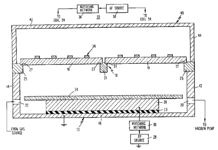
Fiq. 1 is a~ side seetionaJ, view of a plasma
processor in accordance with one embodiment of the
present invention; . ' .
,~ Fig. la is a side sectional view, at right anqles to-
the view of Fig. 1 of a portion of the pl~.sma processor
illustrated zn 'Fig. 1;
Fig. 2 is top view of a coil employing plural
paral7.el linear conductor segments ox elexaents, wherein
all of the currents flow 'in the same, directinr~ through
the segments;
. Fi.g. 2a is a 'tvp view of a portion , of a ~ modified
version of F.ig. 2; .
Fig. 3 is a top view of a coil including paxallel.
segments having currents flowing through them in the same
direction. whereizi the segments are in paths having equa3.
physical and electrical lengths between diagonally
opposite first and second terminals cannected~to, be
responsive to an r.f. excitation source;
ZO Fig. 4 is a top view of a further coil configuration
wherein ail of the currents flow in .para7ae3. branches in
the same. direction between first and second adjacent
terminals connected to an AC excitation source;
Fig. 5 is a top view of a coil arrangement including
multiple paral3e~. coil segments including adjacent..
elements having cnrre~nt flowing through them in opposite
_.' directions, wherein the segments are in paths having ~ .
equal physical and electrical lengths between first and
second terminals at opposite ends of adjacent lead lines;
3d - Fig. 6 is a top view of a col,l including parallel.
e~.ements arranged in a woven pattern so current flows in
opposite directions in adjacent elements; ,
Fig. 7 is a modification of the woven pattern '
structure illustrated i.n Fig. 5;
fig. 8 is a top view of a coil canfigurativn having
CA 02523264 1995-12-05
WO 9611820$ ' ~GTlLTS95115753
plural ca~.I portigns, each occupying a mutually, eXClusi.ve
area on a different individually supported window and ~~
connected in parallel to an excitation source; .
Fig. 9 is a topwiew of a coil including plural
parallel linear segments having differing lengths;
F~.g.. 10 is a top view of a coil .iricluding plural
linear elements connected in series between external
terminals connected to be responsive to an r.f.- source;
Fig. 1i .is a side view. of magnetic flux lines
produced as a result of excitation of the coil
configurations'of Figs. 2-4 and 9; . . .
Fig.. 12 is a side aectianal view of magnetic flux
lines resulting from excitation of the ~coi~3.
configurations of Figs. 5-8 and 10; and
. Figs: 13a-13c are top views of alternate W ndovs
configurations .
Descrit~tion of the Preferred Embodiments
Ref erence is now made to Figs . 1 and 1 ( a ) of the
drawing, wherein a woz~kpiece processor is illustrated as
including vacuum camber 10, shaped as a right -
parallelepiped having electriGa~.ly grounded, sealed . '
exterior surfaces formed by rectangular metal, preferably
anodized aluminum, sidevralls 12 and 14 that extend
parallel to each -other and at right angles to rectangular
metal- sidewalls 13 and. 15. vacuum, chamber ~-~10 also
includes rectangular metal, preferably anodized aluminum,
bottom end plate I6 and rectangular top end plate
structure 1B, including tour individually supported
dielectric, rectangular windows 19 having substantially
' the same size. ' Sealing of these exterior surfaces of . '
chamber l0 is -provided by conventional gaskets (not
shown).
Windows 19, preferably made, of quartz, are
individually supported by one-piece, rigid frame 23, made
of a nax~-magnetic .metal, such as anodized aluminum.
CA 02523264 1995-12-05
wo 9si~szds . pcTius9s~xs7~
to
Frame 23 includes p~:xipheral, mutually perpendicular legs
25 and znterior mutually perpendicular rails 21,
connected to the centers of the legs.. Rails 21 and legs
25 include notches 27, which individuall~i support each of.
'S windows 19 since the side walls of the windows and~the
bottom portions of the windows adjacent the side wails
~it~ in and rest on gaskets (not shown) on the bottoms and
side walls of the notches. Legs 25 of frame 21 are
bonded to side walls ~12~15 of chamber 10. Because
IO windows 19 are individually supported by rails 21 and
legs 25,, the thickness of windows .I9 can be less than
about 2~.5 cm and W tkistand the pxessure differential
between the atmospheric air on the exterior of chamber 1.0
and the vacuum inside the chamber, whzch is typically in.
ZS the 0.~5-5, mil~,iTorz range. If wi.z~dvws 19 were not
individually supported and a single wir~dow were emplpyed,
. such a singl~ .window would have to have a thic3cness of at
least, S cm to be able to withstand the differential
pressure. Such a thick window would sigxiificantly reduce
20 the amount of r.f. field energy that could be coupled
through the windows and would be very expensive. To one
configuration of chamber 10 for processing large
workp~.eces, e_g.,television receiver active matrix liquid
crystal displays having a planar ~ractangular
25 configuration with sides as large as 75 am x 85 cm, each
of windows 19 3~as an area of about 40 cm. x 43 cm.
Sidewall 12 includes port 20, connected to a conduit
(oat shown) leading to a vacuum pump (not shown.) wh~.ch
maintains the intez~~.or of chamber 10 at a pressure on the
. 30 order of 0.5--5 milliToxr: A gas which can be excited to
a plasma, of a type well known in the prior art, is
intzoduced from' a suitable source toot shown) into
chamber 20 via port 22 an sidewall 1~.
Workpiece 2~,., e.g. a: large semiconductor substrate
~35 wafer having a rectangular share as specified supra, is
mounted on metah chuck 26 ~in a p7.ane .parallel to the
CA 02523264 1995-12-05
wo asnszo$ ' rcrms~srxs~sa
m
planes of bottom end plate l6 and windows 19,.and close
to plate 16: An electric field, typically having 'a
frequency of about 3o MHz, is applied to woricpiece 24 by
. r.f, source 28 via impedance matching networ3c 30 and
chuck 26. ~ Chuck ~6 is electrically i3nsulated from,the '
retraining metal parts of chamber 10 because it rests on
electric insulator pad 29. Dielectric end plate
structure 18 carries planar coil 34, connected to,r.f.
excitation device 33 including impedance matching networ7~
l0 36 and r.f. source 38, having a frequency different from
r.~_ source 28, and preferably equal to approximately
13.3 MHz. Both~terminals of source 38 can float or one
of them.can .be grounded to the metal walls of chamber- 10. .
Matching network 36 includes circuitry tuned, to the
f5 frequency of source 38 to form a resonant cr~upling
circuit. Coil 34 ~.s positioned and~responds to source 38
to supply r.f. magnetic lines of flux to the gas coupled.
through port 22, to excite the gas to a.plasma state.
The plasma treats workpiece ~4 to etch the substrate or
20 to deposit molecules thereon.
Planarcoil 34 can have many different
conf~.gurations, as illustrated, for example,, in Figs. 2-
10. Each of these coil configurations includes multiple
linear electrically conducting, metal (preferably silver
25 coated copper) stripe elements ox segments for
inductively supplying magnetic lines a~ flux to the gas
in chamber 10 to sustain and generate a planar plasma
that processes workpieces 24 in chamber lo~_ The linear ,
elements of coil 34 preferably have a rectangular cross
30 section with a braced 'side fixedly positioned ' on
die~.ectx~ic end face structure 18,' although the ri,arrow '
sides of the elements could be fixedly mounted on window
1.9. Coil 34 is basically an, r.t. transmission line
including distr~.buted series inductances resulting from
35 the self inductance of the metal elements and shunt
capaCitances between the metal elements. and the grounded
CA 02523264 1995-12-05
WO 9G/18208 pGTIUS951I5753
chamber exterior walls. To excite and maizitain the
plasma for these purposes, source 3o supplies up~to 3A
amperes to coil 34. ' ' _
To confine and concentrate .magnetic field Wines
~ resulting from current flowing through the linear
canductors of coil 34,~ magnetic shield _ cover '40,
preferably made of aluminum in whzeh x.f. eddy currents
are induced by the r.,f. magnetic flux lines, surrounds
the sides and top of the coil. Cover 40,has a roof 42
10~ and feur sidewalk 44, that are fixedly attached to
vacuum chamber 10.
According to one embodiment, illustrated i,~ci Fig. 2,
coil 34, that extends over all four of windows 19, has a..
configuration including eight elongated, straight,
liziear, metal conducting elements 5x-58 having apposite
ends connected to elongated straight, fetal (preferably .
si7.ver coated copper) leads 59 anal 60 which extend
parallel t4 each other and at right angles to elements
. S1-58. The bottom faces of elements 51-58 and leads 59,, '
60 .are bonded to windows 19, except the portions of
elements 51-58 which span gaps 31 across rail 21, between,
interior edges of the windows, as illustrated in,Fig. la.
Conducting elements SI~58 are, approximately equidistant
from each other '(except for the spacir~g between central y
elements 54 and 55 which is somewhat different because of
center rail 21?. have about the same length and extend
parallel to each other. Leads.5s and,6o include centxal
v terminals 62 and 64, located midway between central
conductors. 54 and S5. Terminals 62 and 64 are
3~ respectively connected to terminal 66 of r.f. source 38
by cable &s and to output terminal 70 of matching network
36 by cable 72.. Matching netwoxk 36 zs connected to
output terminal 74 of r.f. source 3B,.
Tn response to the output of r.~. source 38, current
flows through each of conducting, elemezits 51-54 generally
zn the same direction at any 7.x~,stant to produce w. f .
CA 02523264 1995-12-05
wo ~sns~os ~ . ~crms~s~zs~s3
13
magnetic flux lines 124, x.28, 130 and I32, Fig. 1.l.
wBecause the lengths Qf each,of conducting~elemants 51-58
. is a re3.atively small fraction, e..g. about 1/I6th, of a
wavelength (a) of 'the frequdncy derived from r_ f _ source
38, the instantaneous. current arid voltage variations
across each of the conducting elements is net
substantial. Because central conducting elements 54 and .
55 have.the same I~ngth, same cross sectional geometry
and are equispaced from terminals 62 and 64, the lengths
14 of the current paths formed by the transmission lines
. from tez~minal 62 to terminal 64 through conducting .
elements 54 and 55 axe the same, whereby the t~c~agnetic
flux densities resultizig from the substazitially equal. RMS
.amplitude r.f. curre'rlts flowing through conducting,
I5. elements 54 and 55 are approximately the same.
Similarly, slightly off -center conducting elements 53 and
56 have equfl hength transmission lines and eurx~ent paths
between terminals 62 ' arid 6-4 , so the magnetic flux
densities resulting. from' the substantially equal RMS
20 amplitude currents Flowing through them are about equal.
Because the lengths of the transmission lines and
current paths through conducting elements 53 and 55 are
somewhat greater than those through elements 54 and 55,
there is a tendency far. the RMS values of the r,f.
25 currents flowing through elements 53 and. 55. to be
somewhat ~.ess than those through elements 54 .and 55,
whereby the magnetic flux densities derived from eJ~emer~ts
53 and 56 tend to'be less than those from elements 54 and
55. Hy the same reasoning, magnetic flux densitie s
30 resulting from r:f. excitation of conducting elements 52
and 57 are approximately the same and tend to , be less
than those resulting fz-om current flowing through
conducti~zg elements S3 and 56; the same is true for
conducting elements 51 and 5s.~
3,5 . As a result of the differential lengths of the
transmission. lines a.nd the resulting differences 'in .
CA 02523264 1995-12-05
Wo 9sixs2o8 pcrrusssns~s3
14
current, path lengths frbm terminals 62 and 64 through
different ones of elements 51-S8 there are differences in
the excitation and distribution of. the plasma in chamber
z0_ this is iikely.to lead to uneven plasma processing
of the Large surface area workpiece because there is
greater plasma density in,the workpiece central region
(beneath elements 54 and 5S) thari the workpiece periphery
. (beneath elements 51 and 58).
According to -one, aspect of the invention, the
to lengths of the transmission lines iz~cluding elements 51
58 are approximately eleatrieally equalized by proWding
the different 'lines with reactances having different
values. Since the self inductance of a single electric
lixie is inversely proportional ' to the line .doss
seGtior~al area and the inductance of a line increases as
the ~.ine length inczeases, the lines closest to terminals
5~ and 64 ean~be made electrically longer by decreasing
the cross sectional. areas thereof relative to~the cross
sectional areas of the lines farther from the terminals.
zt is also desirable to maintain the electrical length of
each of elements 51-56 the same so the RMS voltage and
current variations across them are equalized to provide
the same plasma .distribution below these elements. .
To these ends, the cross seCtior~a~. areas of leads S'9
and 50 progressively increase between adjacent pairs of
' segments 55-58 and 51.54 while~the crass sectional areas
of segments S1-58 are the 'same. Hence, 7.eads 59 and 60
have re~.atively small cross sectional areas between
'segments 55 and 56 as well as between segments 53 and 54
3o and relatively large. cross sectional areas between
segmez~ts 57 and 58 as well as between segments 5I and 52.
Alternatively, capacitors 81-88 are connected in
series with elements 57.-58 to equalize tl~e lengths of the
ltransrnissic~n lines. As illustrated in fig. 2a,
capacitors 8~.-88 are connected in series with elements
51-58 arid lead 59, at the end of each, element adjacent
CA 02523264 1995-12-05
WO 96118108 ~ ~ PGT/US95115753
the lead. These locations for capacitors 81-88 do not
affect the effecti~re physical lengths of elements 51-58
because of the relatively small physical size Qf the
capacitors.
5 To enable the phase. of the currents in each of
elements 51-58 to be generally the same (either leading
or lagging the voltage across the element? the geometry
of elements 51-58 and.the values of capacitors 41-88 are y
selected so the net impedance at the frequency of source
10 . 3B of each of the -branches ~.ncluding e3~ements 51-5B is of
the same reactar~ce type , i . a ., either - inductive or
capacztive. If the inductive impedance of elements 51-58
. ~is dominant, each of series capacitors 81-88 has a .
relatively large value, to provide a relatively small,
15 capacitive impedance in series with each element_ Hence,
capaaitars 84 and 85 in series with elements' S4 and 55
have smaller values than capacitors 83 and 86 in series
with elements 53 and 56, capacitors 83 and 8~ in series
with elements 53 . and 56 have smaller values than
28 Capacitors B2 and 87 in series with elements~52 and 57,
etc.. so that capacitors 81 and 88 in sex~.es. with elements
.51 and 58 have the largest val-ues or may be eliminated.
.It, however, the dominant impedance in the branches
' including elemezzts.51-58 is capacitive, the values of
, capacitors 81-68 are. relatively small to provide high
capacitive impedances; the values of pairs of capacitors
84, 85, 83,_86, 82, 87, 81, 88 progressively decrease in
the order.named.
Reference is now made to fig. 3 of the drawing,
wherein coil 34 is illustrated -as including. linear
conducting elements 51-5B, arranged and.constructed the '
same as conducting elements 51-S8 ref Fig. 2. Tn Fig. 3
conducti2~g elements 51-58 have opposite ends. connected td
straight elongated metal leads 9o az~,d, 92 that extend
paraJ.lel to each other and at right angles to conducting
elements 51-5B. Leads 90 and ~~ have large cxoss
CA 02523264 1995-12-05
WU 96!18208 . PGTI(JS95115153
I6
sectional areas resulting in small inductarxces that do
not introduce,appreciable transmission line lengths ox
phase shifts ~.n the. paths leading to and from elements
51-5B_ Lead 9D includes a portion which ends at terminal
94 and extends slightly beyond caaductor 51; similarly,
lead 92 includes a portion which ends at terminal 95 and
extends slightly beyond lead 50 . Terminals 94 and 96 axe
connected to the same leads and circuitry as terminals 62 .
and 64. respectively. ~ w
1o An advantage of the structure illustrated in fig. 3 _
is that the current path through each of conducting
elements 5~.-58 between terminals 94 and 95 has the same
physical and electr~.cal length. , xhereby, the, RMS
amplitude of the AC current flowing in each of cor~.r3.uct~.ng
~.5~ elemexxts 51-58 isvirtually the same. Because the RM5
amplitude of the AC current ~~~.owing in each of conducting
elements 51-58 is about the same, the magnetic f~.ux .
densities resulting from excitation of these conduct~.ng
elements by the r . f . source 3 8 i, s about the same
20 ~ .The magnetic ~lux lines resulting from x.f.
excitation of conducting elements 57.-58 produce r.f.
. ,'. magnetic flux lines 124, 1.28, 130 and 132 (k'ig.' 13? in
the gas introduced into chamber la, to excite the gas to
a plasma having equal numbers of positive and negative
25 charged tarriers_ Because, of the resulting molecular
flux in the plasma, the plasma functions as a single turn
secondary winding ~of a trans~ormex including, as its
. primary windings, conducting elements 51-58. The . .
conducting properties of the plasma cause r.f. magnetic
3a flux lines 1.24, 128, ~3o and 132 to .lie asymmetrical,
i.e., the magnetic flux l~.nes extend above windows I9
into the atmosphere to a considerably greater extent than
blow- the windows ' into vacuum chamber to . The charged .
carriers disperse through the,gas to cause the volume of
35 gas to 7oe a pzasma for treating substrate or workpiece
24.
CA 02523264 1995-12-05
'W096I1820S . PGT/DS95/IS7~3
17
Reference is now made to Fig_ 4 of the drawing,~a
further configuzation of coil 34, including elongated
straight leads 134 az~d 135, that extend parallel to each
other and include end terminals 138 and 14 D , respectivexy
cdnnected~to r.f. exciting device 33 via cables 72 and
68. Extending ~ betv~reen leads . 134 and 136 .are linear,
paraJ.lel elongated conducting elements 51-&e ~ which are
identical tb the corresponding elements of Figs. 2 and 3.
Elements 51-58 are driven by r.f. exciting device 33 so
that at any instant of time, r:f. parallel currents
generally flow through them in the'same direction. Leads
134 and 136'and elements 51-58 of Fig. 4 are arranged so
end terminals 138 and 140 are at the same ends of the
leads relative to the conducting elements and the
15, terminals are spaced from each other by the lengths of
the conducting elements. To enable the coil
configuration of fig. 4 to include equal electrical
length transmzss~.on lines 'through elements 51-58 from
tez~ninals 138 and 140 via leads 134 and 236, the cross
section geometry of different parts of the leads can
d~ffex, as discussed in connection with Fig. 2, and/or -
capacitors can be connected in series with elements 51-58
as discussed in connection with Fig. 2a.
a result. of the currents flowing in like
direetioz~s through conducting elements 51!59 in each of
Figs. 2-4, there is at least one,magnetic~flux line 124
(Fig_ 11) surrounding each of the conducting elements and
thexe is a cumulative effect caused by the interact~.on of
magnetid fluxes resulting from.the currents flowing in
elements 51-58. Thereby,' a highly concentrated, evenly
distributed, magneta.c ~.geld is provuded in the plasma
beneath windows 1~. Fox example, the like directed
currents flowing through conducting elements 52 and 53 or
thxough elements 56 and 57 cause these two pairs of.
conducting elements to be surrounded by magnetic flux
lines 128 and X29, respectively. The interaetior~ between
CA 02523264 1995-12-05
we 961i$xoa fCTICtS951I5753
18
the magnetic fluxes resulting from currents fla~aing in a
lake direction in conducting eZemezits 5S-58 causes these
conducting elements to be surrounded by magnetic flux
lines 130. ~An interaction between the magnetic fluxes
resulting from currents flo~saing in a like direction ,
' through all of conducting elements 51-5~9 causes elements
5Z-58 to be surrounded by magnetic flux lines 132. The
- concentrated magnetic flux lines resulting from the
excitation patterns of conducting elements 51-58 provide
1~ a relatively uniform distributvon of. plasma in chamber ZO . -
beneath top end plate structure l8 so there is an even
distribution of~ etchant or deposited molecules on
workpiece 24.
According to further embodiments of the invention,
15, illustrated iii figs . 5--7, the' conducting elements of tail
34 are arra~ngeci so current . generally f lows in adj scent .
linear conducting elements of the co~.l in spatially
opposite directions at any instant of time. The
structure - of Fig . 5 has the advantage of providing
20 current paths with equal physical,azid electrical lengths
through each of the~condnctors between opposite terminals
of r.f. excitatzon device 33. While the magnetic fluxes
coupled to the plasma lay the structures of. Figs. 5-7 have.
lower density than those of Figs. 2-4,- in some instances
25 xt may be.desirable to tailor the flux density to certa~,n
regions of the plasma as can- be more easily provided with
the structures of Figs. 5-~7 thar~ those of Figs . ~ 2,~
'fhe stru~t~,re of fig. ~5 includes spatially adjacent
and parallel, elongated stxaight~ leads lOD and 102,
30 respectively having. terminals lD4 and X06 at spatially
oppasit_e ends thereof, connected to opposite terminals 56
and 72 of r.f. excitation device 33.~ Coil 34 of Fig. 5
includes four segments n13., 112., 113 and 214, each
including a pair~of elongated; linear straight parallel .
35 conducting elements, having opposite end terminals
respectively connected to leads 10p~ and 1D2. heads 10p
CA 02523264 1995-12-05
WO 961I8~08 ~CT/US95115753
19
and 102 are generally positioned to one side of segments
~.1~.-114 so the conducting elements extend in the same
direction to the side of interior lead 102. The coil
segments arid conducting elements are arranged so coil
segment 111 includes conducting elements 115 and 117,
coil segment W2 includes conducting elements 118 and
119, cflil segment 213 includes conducting elements 12.0
and 121 and coil segment 11~ .includes conducting elements
122 anrl 123. The,parallel conducting elements of coil
segments 111-114 are connected. to each other by
conducting elements 125 that extend parallel to leads 'loo
and 102. Conducting, elements 11G-123. are generally
equispaced from each other so that, for example,
conducting element 117 of coil segment 111 is spaced the
same distance from conducting element 118 of coil segment
11.2 as it is spaced from conducting element 116 of coil ,
segment .111. Each of the transmission lines including
coil segments 111-114 has the same physical and
electrical length between apposite terminals ~.0~ and 106
because (1) of the geometry of the layout of coil
segments 117.-ll~~ and leads 100 and. 102, (2) each of . .
segments 111-11~ has the same cross sectional and
longitudinal geometry and (3) leads 100 and 102 have the
same cross sectional and vlongitud~.nal geometries.
A further configuration for providing spatially
parallel conducting elemer~ts that are electrically
cdnnected 'in parallel and have adjacent conducting
elements. with currents flowing generally in. apposite.
directions is illustrated in Fig. 6 as a woven pattern
3D including straight elongated linear leads 150, 151, 15~..
and 1,53, in combination with straight elongated linear
canducting~ elements 151-158. .Leads 15n-1$3 extend
spatially paralldl to each other, and at right angles to
conducting elements 161-168 that are gez~erally equisnaced
from each other and spatially extend parallel to each
other. L~eacis 15b, 151 are on one side of elements 7.61-
CA 02523264 1995-12-05
W'O 961182p8 . ~ - ~~ T1U595115753
z68 while leads 152 and 153 are nn the other side of
these elements. . Leads 151 and 153 aze respectively
connected by cables 154 and 1S5 tt~ a first terminal 156
of r.f. excitation device ~33 while leads l5fl and 152 are
5 respectively connected by cables 1S7 azid 158 to a second,
opposite t$rmina1~159 of the device 33. Alternate equal.
length conducting elements 161, 163, 165 and 157 are
electrically connected between leads 150 and 153, whi~Ie
the remaining, equal length conductixzg elements x.62, 3.6~,.
~,D ~66~ and 1Ge are electrically connected iii parallel
between leads 15l and 152._ $ecause elements 161, z63,
16S and 167 are connected to.exterior leads 1S0 and 153
and .elements 162, 164, 166 and 168 are connected. to
interior leads 151 and zS2, the former elements are
15 _ longer than the latter_ Thereby, at any instant of time,
currents~generally flow in the same direction through
conducting elements 161, 153, I56 and 167, which ~.s
opposite from the i3irection cuxrents general~,y flow
through, conducting ~.lements 162, 164, 166 and 168.
20 Magnetic flux paths similar to those provided ~by the
structure illustrated in Fig. 5 are thus established by
the~coil arrangement of Fig. 6. Because the physical
distance between terminals 156 and 159 via the
transmission lines snc7.uding e3.ements 161-158 differ, it
' is praferable.to change the crass sectional geometry of
Zeads~150-153 in a manner sirttilar t4 that described for
Fig, 2 or to connect capacitors in series with elements
161-169 as described for Fig. 2a.
The woven coil arrangement of Fig. 6 can be
- modified, , as illustrated in F~.g. 7, so .each of~ the
conducting elements ha~.the same Length. To these ends,
the woven coil structure of. Fig. 7 .includes elongated,
parallel straight leads 170, 171, 172 and 173, in
' combination with elongated, parallel straight conducting
elements x.81-188. Leads 170-173 extend at right angles
to equispaced conducting elements 18z-n88_ Exterior
CA 02523264 1995-12-05
WO 9411$Z08 _ P~YU59S/I5753
21
leads 170 and 173 are connected to terminal 190 of r.f..
.excitation device 33 by cables 19~ and 192, respectively_
anterior leads 171 and 172 are cQrnn,ected to terminal 193
of r.f_ excitation device 33 by cables 194 and '195,
respectively.~.Conductir~g elements 181, 183, 185 and 1s7 ' ,
are electrically connected in parallel across leads~l7p
and 192; while conducting~elements 182, 184, 18G and 18s
are electrically connected in parallel across leads 17p
and 172. Thereby, generally oppositely directed currents
0 flow through adjacent.pairs of leads' 181-188 so that, for
example,. when current is f3.owing through conducting
eleutent 182 from lead 170. to lead 172, current is flowing
through conduct~.z~g elements 7.81 and 3.83 from lead 173 to
lead 1'71. Hence, current f~,ows in apposite directions in
~~ adjacent cc~nduct~ing elements in a similar.manner in the
embodiments of Figs. 6 and 7. , ..
In response to.excitation o~ the coils illustrated
in Figs. 5-7 by r. f _ excitation device 33, magnetic lines
of flux, as illustrated in Fig_ IZ are produced. In Fig_
12; magnetic flux, ~ lines 38'1=388 are respectively
associated with the equal ~.ength conducting elements 3.81-
188 of Fig. 7;'3t is to be understood that~s,imilax flux
line patterns are obtained for conducting elemerats 1Z6-
123 of Fig. 5 and conducting_elements 16z-168. ~ecaus.e
current floras in opposite directions in adjacent ones of
~e~.ements .181-188, the magnetic flux lines resulting from
these.currents buck each oth~x~ so there is no interaction
of flux patterns 381-388 and there is flux null between
adjacent. conducting elements. - Since there is no
3D conducting element or magnetic member on the. exterior
sides of conducting elements x.87. and 188, magnetic flux
lines 381 and 388 bu~.ge away from the center 'of coil 34.
Hecause conducting elements. 18~ and 185 are spaced
farther apart than other pairs of the conducting elements
35~- (due to rail 21), magnetic flux lines 384 and 3s5 bulge
i toward center dielectric rail 21. The interior
CA 02523264 1995-12-05
WO 96/I8208 ~CTIt159a/15753
22 .
equispaced positions of cbnducting elements x.82, 183, 186. .
ahd 18~ cause ~lux lines 382, 383, 386 and 387 to have
' about the same density and ~spatzai configurat~.on.
The coil structures illustrated in figs. 2-7 are
, designed to extend over all four windows 19 of top_end
plate structure 18: In certain instances,, howe_ ver, it is
desirable to provide individual coils on eaeh.of windows
~.9. To this erid, any of the coil structures described in
connection with Figs. 2-7 can be ,connected in parallel
and separately overlay each of~windows 19, as illustrated
in Fig. 8. In the particular embodiment of Fig. 8, each
of windows 19 is overlaid by separate.coil segments 2~1,
~D2, 203 and 204, each constructed generally in the .
manner described irx connection with Fig. 4. Adjacent
' int~rzor leads 205 and 206 of coil segments 201 and 202
are connected tQ terminal 20'7, connected by cable 208 to
termiizal ~p9 of r.t.~ excitation device 33. .Terminal 209
is also connected by cable 211 to terminal 212,Iinrturri
connected tQ.interior adjacent leads 213 and 214 of coil
segments 203 and 204. Exterior leads 21,5 and 215 at coil
segments 201.and 202 are connected by cable.217 to the '
other terminal 218 of r.f. excitation device 33.
Terminal 218 is also connected by cable 219 to eXterior
leads 220 and 221 of coil segments 203 axi~d 204. Thereby,,
segments 20I-204 of coil 34, as illustrated in ~'ig. 8,.
are driven in parallel by device 33.~ Each o~ the ccih
segments~has electrically parallel conducting elements
with relatively short lengths (rzo more than 1/~.6th of a
wavelength of the wave derived by device 33) to minimize
' the like3.ihood of voltage~and/or current nulls therein.
Eecause the four coil segments 201-204 are relatively
short transmission lines it may not be necessary in
certain ~.nstaz~ces for all of the indivzc~ual transmission
lines on the individual windows ~Z9 to have the same
length.
CA 02523264 1995-12-05
WO 961XSx08 PCTl0595I15T53
23
In each Qf tk~e embodiments of Figs. 2--s, the
conducting elements of the various planar coils have
equal physical lengths. It is not necessary, however,
for the condz~cting elements to have equal physical
lengths, and in some instances it may be desirable fdr
the physical lengths ~ thereof to differ. ' In the
embodiment Qf Fig. 9, the structure of k'ig_ 2 i.s modified
to include arcuate leads 226 and 229 between which extend
spatially parallel elongated straight cpzzdueting elements
231-23B having differing physical lengths. Midpoints of
arcuate leads 226 and 228 include terminals 240 and 241,
respectively connected to opposite polarity terminals of
r.f. excitation device 33. Currents flow in parallel in
generally the same direction through conducting elements
35 231-238. The structure of Fig. 9 is employed to.enable
the- plasma in chamber 1o to have certain special spatial
canfigurations~for treating substrates having appropriate
surfaces_
While it is desirable to pro~ride elements 231-238
with different physical lengths, the electx~.cal lengths
of the, transmission lines including these elements are
preferably the same, a result which can, be achieved by
use of the structures described in connection with Fig.
2 or 2a. Even though elements 23Z-238 are illustrated as
being approximately equispaced'from each other, this. is
not necessarily the case- for the configux~a~tions of any of
Figs. 2=9.
A magnetic flux pattern similar fo that of Fig. 12
can be pxovided by forming coil: 34 as plural series
, conduct~.ng elements, as illustrated in Fig. 10. The coil
of Fig. 10 includes conducting elements 241-248 that
extend spatially in parallel to ,eack~ other, have
approximately equal lez~gtk~s and have adj acent ends
connected together by conducting elements 249 and 250.
' Conducting elemerits ~2d1 and 248 are connected to end
terminals 252 and 254, in. turn connected by appropriate
CA 02523264 1995-12-05
WQ 96!18208 ' PG~Y(J595I15753
24
cables to opposite end termiz~als of r,f_ excitation
w device 33. Current thus flows generally iri opposite
directions in~ad~acent conducting elements 241-248, as ~ ,
result of the sinuous or serpentine relationship of these
conducting elements.. The structure of Fig. .10 has a
substantial disadvantage relative to the' structures o~
Figs. 2-~ because of its long physical and electrical
length, whereby there is a tendencyWar voltage and
current nuJ,ls along the length of the coil formed by
elements 241-248.' These nulls cause uneven distribution v
of magnetic f~.ux acting on the gas ire chamber 10. This ,
problem is obviated by the parallel structures of Figs.
' Z-9,-all of which have conducting elements in parallel ,
with each other across the terminals Qf r.f. excitation
device 33 and lengths that are about 1/l6th wavelength of
the wave derived by device 33. The structures of~all of
Figs . 2-ld have the advantage of being. planar coi,l.s
having exterior terminals, outside of the conducting
elements for ease of.cor~nection so problems. associated
with.spiral planar coils having oz~e interior texzninal are
avoided. All of'these planar coils, as well as spiral
planar coils, can be used as four individual coils,
connected in parallel, on the four wzndows~ 19 of end '
plate structure 28, as described in connection with Fig.
8. .
While ez~d plate structure .18 preferably includes
four rectangular dielectric~wzndows having the same size
and positioned in the guadrants~of a rectangular frame,
other individually supported dielectric window
~ Configurations, e.g.. as schematically illustrated ire ~ .
Figs. 13 (a) , Z3 (b) and L3 (c) , can be ect~ployed.
Individually supported dielectric windows 302-310, fig.
13 (a) , in frame. 31.7, have different sizes and shapes such
that, rectangular per~.pheral ~wzndows 302-308 have
different lengths, extend. at mutually right angles and
surround .interior .square window 3~,0. In Fig. 13(b)
CA 02523264 1995-12-05
wo 9snszos ~crmsssms»s
is
diamond shaped, centrally located dielectric window 312
and triangle shaped.exterinr dielectric c~indows 314 are
individually supported in frame 315 , frame, 318 , P'ig .
13(c), individually supports three rectangular windows
320, each.having the same size and parallel Zong sides-.
Planar coils, as illustrated in Figs. 2-10, axe laid an
the windows of Figs. 13(a), 13(b) and 23(c). .
While there have been described and illustrated
specific embodiments of the invention, it will be clear
that variations in the details of the embodimez~ts
specifically illustxated and described may be made
. without departing from the true spirit and scope of the
invention as defined i,n the appended claims. ,