Note: Descriptions are shown in the official language in which they were submitted.
CA 02523411 2005-10-21
A Double-sided Pluggable Backplane
Field of the Technoloizy
The invention relates to a backplane used in a communication device, in
particular to a double-sided pluggable backplane.
Background of the Invention
At present, with high requirements for integration of a communication system,
it
has become a developing trend to directly multiply the number of slots with a
double-
sided pluggable backplane in backplane technology. Multiplication of the
number of
slots improves balancing of configuration granularity of system services on a
board,
directly leading to flexibility and reliability of design as well as
feasibility for multi-
production integration.
Figure 1 schematically illustrates connection of a double-sided pluggable
backplane and boards according to the prior art. As shown in figure 1, a front
board
100 is plugged into a front backplane connector 111 of a double-sided
pluggable
backplane 110 by means of a plug 101, and a rear board 120 is plugged into a
rear
backplane connector 112 of the double-sided pluggable backplane 110 by means
of a
plug 121. Front board 100 is in alignment with the corresponding rear board
120.
However, front backplane connector 111 and rear backplane connector 112 are
located at different horizontal levels, meanwhile plug 101 of front board 100
and plug
121 of rear board 120 are located at different horizontal levels too, i.e.
they are
staggered up-and-down. Although front backplane connector 111 and rear
backplane
connector 112 can have uniform definitions for interface contact pins, yet
they have
different horizontal locations, thus front board 100 and rear board 120 can
not be
interchangeable on a double-sided pluggable backplane.
It could be seen this kind of double-sided pluggable backplane has an
insurmountable disadvantage. More specifically, a board in a front slot cannot
be
interchanged with that in a rear slot, which is similar to back-to-back
integration of
two frames in essence.
1
CA 02523411 2005-10-21
Aiming at the above disadvantage, a design idea has been proposed that adopts
special backplane connectors to make boards interchangeable at fore-and-aft
slot
positions.
Figure 2 is a schematic diagram illustrating an interchangeable double-sided
pluggable backplane and boards according to the prior art. As shown, a front
board
200 is plugged into a front backplane connector 211 of a double-sided
pluggable
backplane 210 by means of a plug 201, and a back board 220 is plugged into a
rear
backplane connector 212 of double-sided pluggable backplane 210 by means of a
plug
221. Both of front backplane connector 211 and rear backplane connector 212
comprise a power supply interface and a signal interface, and they are located
at the
same horizontal level. Meanwhile, front backplane connector 211 and rear
backplane
connector 212 have uniform definitions for interface contact pins, so front
board 200
and rear board 220 are interchangeable on the backplane.
Here, front backplane connector 211 and rear backplane connector 212 on
double-sided pluggable backplane are the same special backplane connectors,
and
they are aligned in the up-and-down position and fore-and-aft position
absolutely. The
depth of the contact pins of front backplane connector 211 and rear backplane
connector 212 must be less than or approximately equal to half of the
thickness of the
backplane, and the contact pins must be insulated from each other.
The above-mentioned double-sided pluggable backplane has rather high
requirements for its circuit board. The thickness error of the circuit board
must be
exceedingly tiny, otherwise it cannot be guaranteed that the depth of the
contact pins
of the special backplane connectors is less than or approximately equal to
half of the
thickness of the backplane and that the contact pins are insulated from each
other. The
speciality of the backplane connector, along with the special requirements for
designing, manufacturing of the printed circuit board in the backplane and
machining
of the backplane directly bring about some insurmountable difficulties, such
as
costliness, difficulty in processing and so on. Therefore this kind of double-
sided
pluggable backplane is still in the stage of designing rather than being
applied in
practical manufacturing.
Summary of the Invention
2
CA 02523411 2005-10-21
In view of this, an object of the invention is to provide a double-sided
pluggable
backplane which can realize interchangeability of front boards and rear
boards, reduce
design and manufacture difficulty of the double-sided pluggable backplane and
lowers
design cost of the board.
To achieve the above object, the technical scheme of the present invention is
implemented as follows.
A double-sided pluggable backplane has one side on which one or more than one
front backplane connector is disposed according to width of plot positions and
the
other side on which one or more than one rear backplane connector is disposed
according to width of plot positions. The front backplane connector and the
adjacent
rear backplane connector are located at the same horizontal level on the
double-sided
pluggable backplane and staggered right-and-left in turn. Meanwhile the front
backplane connector and the rear backplane connector have uniform
specifications
and the same contact pin definitions.
The front backplane connector and the adjacent rear backplane connector may
share width of one slot position.
Each of the front and rear backplane connectors may comprise a power supply
interface connector and a signal interface connector.
Both the power supply interface connector and the signal interface connector
may be common backplane connectors.
Each of the front and rear backplane connectors may comprise guiding/error-
preventing pins on upper end and lower end.
From the above technical scheme of this invention, it can be seen that the
double-sided pluggable backplane according to the present invention can
realize
interchangeability of front boards and rear boards easily with common
backplane
connectors by staggering the front and rear backplane connectors left-and-
right. The
double-sided pluggable backplane according to the invention has no special
requirements for design and manufacture of printed circuit boards and
machining of
the backplane, which decreases cost of production and difficulty on
processing. At
the same time, interchangeability of front boards and rear boards reduces
design cost
of boards.
3
CA 02523411 2005-10-21
Brief Description of the Drawings
Figure 1 is a schematic diagram illustrating connection between a double-sided
pluggable backplane and boards according to the prior art.
Figure 2 is a schematic diagram illustrating an interchangeable double-sided
pluggable backplane and boards according to the prior art.
Figure 3 is a schematic top view illustrating a double-sided pluggable
backplane
according to a preferred embodiment of the present invention.
Figure 4 is a schematic front view illustrating the double-sided pluggable
backplane shown in figure 3.
Detailed Description of the Invention
Now, the present invention will be described in detail hereinafter with
reference
to an embodiment and accompanying drawings.
It is not necessary to adopt special connectors for double-sided pluggable
backplane on the double-sided pluggable backplane according to the invention.
Instead, narrow backplane connectors may be adopted. In an embodiment, common
ZD connectors may be employed. The width sum of two connectors may
approximately equal to the width of one slot position. In this invention, it
is not
required that the width sum of the two connectors accurately equals to the
width of
one slot position, and thus this invention can be realized with various kinds
of
common connectors, leading to easiness and flexibility in implementations.
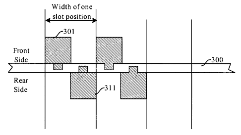
Figure 3 is a schematic top view illustrating a double-sided pluggable
backplane
according to a preferred embodiment of the present invention. As shown in
figure 3,
in an interval of an approximate one slot position on a double-sided pluggable
backplane 300, the left half of the interval is occupied by a front backplane
connector
301, and the right half of it is occupied by a rear backplane connector 311.
Obviously,
the right half of the interval may be occupied by front backplane connector
301, and
the left half of it may be occupied by rear backplane connector 311.
If the interval of one slot position is not enough for the width sum of two
backplane connectors, the front and the back slot positions may be staggered
left-and-
right in order to ensure the double-sided connector being installed
horizontally.
4
CA 02523411 2005-10-21
Generally, male connectors are adopted on the front and rear backplane
connectors of
the double-sided pluggable backplane, and female connectors are adopted on
boards.
Figure 4 is a schematic front view illustrating the double-sided pluggable
backplane shown in figure 3. As shown in figure 4, the front backplane
connector and
the rear backplane connector on the double-sided pluggable backplane in this
embodiment respectively comprise a power supply interface connector and a
signal
interface connector which is a common ZD connector. The front backplane
connector
of double-sided pluggable backplane 400 according to the present embodiment
comprises a power supply interface connector 401 and a signal interface
connector
402. Power supply interface connector 401 can be located either above signal
interface connector 402 or below it, providing the interface contact pin
definitions of
the backplane connector are the same as those of the board. In figure 4,
reference sign
403 denotes a power supply interface connector of a rear backplane connector,
while
reference sign 404 denotes a signal interface connector of the rear backplane
connector. Power supply interface connector 403 is identical and disposed at
the same
horizontal level with power supply interface connector 401 while signal
interface
connector 404 is identical and disposed at the same horizontal level with
signal
interface connector 402, and identical interface connectors have absolutely
uniform
contact pin definitions.
To exactly plug the boards into the front/rear backplane connectors of the
double-sided pluggable backplane, guiding/error-preventing pins are set on
both the
upper end and lower end of each front/rear backplane connector in this
embodiment.
The guiding/error-preventing pins may be set at other positions of the
front/back
backplane connector according to practical conditions.
It can be seen the front and rear backplane connectors of the both-sided
pluggable backplane according to this embodiment are disposed at the same
horizontal level and have uniform contact pin definitions, which makes it not
necessary to design front boards and rear boards respectively. Since the front
and rear
backplane connectors usually employ male connectors, the only requirement for
connectors on boards is that they employ female connectors corresponding to
the male
connectors of the front and rear backplane connectors, thus interchangeability
of the
front board and the rear board is achieved and design cost for boards is
lowered.
CA 02523411 2005-10-21
In addition, in this embodiment, the number of front backplane connectors on
the
both-sided pluggable backplane can be either the same as or different from the
number of rear backplane connectors according to the actual requirements of
communication services.
It can be seen from the above embodiment that the double-sided pluggable
backplane according to the present invention can realize interchangeability
between
front boards and rear boards easily with common backplane connectors. The
double-
sided pluggable backplane according to the invention has no special
requirements for
design and manufacture of printed circuit boards and machining of the
backplane,
which decreases cost of production and difficulty on processing. At the same
time,
interchangeability of front boards and rear boards reduces design cost of
boards.
6