Note: Descriptions are shown in the official language in which they were submitted.
CA 02523555 2005-10-25
Description
1115P44CA01
ATTENUATOR DEVICE, AND OPTICAL SWITCHING DEVICE
Technical Field
The present invention relates to an attenuator device and
an optical switching device and, more particularly, to
an attenuator device and an optical switching device
utilizing an offset-dispersion double spectrograph.
Background Art
In the prior art, there has been known the attenuator device
utilizing the offset-dispersion double spectrograph.
This offset-dispersion double spectrograph may also be
called the offset-dispersion type double monochromator
or the zero dispersion double spectrograph. In the
attenuatordeviceutilizingtheoffset-dispersion double
spectrograph, an input beam is sequentially subj ected to
two wavelength dispersion effects (in the opposite
directions),thediffracted beamafter receivingthefirst
wavelength dispersion effect and before receiving the
second wavelength dispersion effect is subjected to an
attenuation operation. Then, the attenuated beam is
subj ected to the second wavelength dispersion effect and
is then output to the outside.
In the attenuator device utilizingthe offset-dispersion
double spectrograph, as described in JP-A-2002-196173,
the attenuation operation is executed by using a micro
1
CA 02523555 2005-10-25
mirror array. Specifically, the micro mirror array is
so configured that the diameters of the individual micro
mirrors may be smaller than the spot diameter of beam (to
be operated) incident on the micro mirror array, and that
the multiple micro mirrors may be arranged in the spot
diameter of the beam to be operated. Moreover, the
attenuation operations is performed by inclining some of
the plural micro mirrors positioned in the spot diameters
in directions different from the output direction and by
guiding to outside of the optical path, i . a . , discarding
a part of the beam to be operated. Moreover, the beam
discarded at that time is detected by a sensor to monitor
the spectral information, so that the number of micro
mirrors to be inclined in the directions different from
the output direction is controlled on the basis of that
spectral information.
In the attenuator device utilizing the offset-dispersion
double spectrograph described in JPA-2002-196173, the
micro mirror array is so configured that the diameter of
the individual micro mirrors may be smaller than the spot
diameter of the beam (to be operated) incident on the micro
mirror array, and that the multiple micro mirrors may be
arranged in the spot diameter of the beam to be operated.
This arrangement raises a problem that the configuration
of the micro mirror array is complicated.
Moreover, the arrangement imagines the single output port
2
CA 02523555 2005-10-25
so that it cannot meet the function using the plural output
ports selectively.
Disclosure of the Invention
The present invention has been conceived in view of the
background thus far described, and has an obj ect to provide
an attenuator device and an optical switching device
having simpler configurations. Another object of the
present invention is to provide an attenuator device and
an optical switching device, which also have a function
to select an output of beam of an arbitrary wavelength
range from a plurality of output ports.
Inordertoachievetheabove-specified objects, therefore,
an attenuator device according to claim 1 comprises an
output port, a discarding port arranged adj acently to the
output port, diffraction means whichdiffracts an incident
beam in various directions according to the wavelength
thereof, and output direction adjusting means which
adjusts an output direction of a diffracted beam for each
of wavelength ranges output from the diffraction means,
wherein the output direction adjusting means adjusts the
output direction of the diffracted beam so that the
entirety of the diffracted beam may be output to the output
port or the discarding port or so that a part of the
diffracted beam may be output to the output port whereas
the rest may be output to the discarding port, and wherein
3
CA 02523555 2005-10-25
the discarding port discards the diffracted beam so that
the diffracted beam may not return to the side of the
diffraction means.
An attenuator device according to claim 2 comprises an
output port, a discarding port arranged adj acently to the
output port, diffraction means which gathers a plurality
of incident beams of different wavelength ranges into one
predetermined direction, and output direction adjusting
means which adjusts an output direction of a diffracted
beam output from the diffraction means,
wherein the output direction adjusting means adjusts the
output direction of the diffracted beam so that the
entirety of the diffracted beam may be output to the output
port or the discarding port or so that a part of the
diffracted beam may be output to the output port whereas
the rest may be output to the discarding port, and wherein
the discarding port discards the diffracted beam so that
the diffracted beam may not return to the side of the
diffraction means.
According to claim 3, an attenuator device of claim 1 or
2,whererin the output direction adjusting means adjusts
the output direction of the diffracted beam through the
diffraction means so that a part of the diffracted beam
may be output to the output port whereas the rest may be
output to the discarding port, and in that the diffraction
means inversely diffracts the diffracted beam which has
4
CA 02523555 2005-10-25
been adjusted in the output direction by the output
direction adjusting means.
According to claim 4, an attenuator device of any of claims
1 to 3, further comprising detection means which detects
a quantity of a beam incident on the discarding port, and
' control means which controls the adjustment of the output
direction of the diffracted beam for each of the wavelength
ranges in the output direction adjusting means, according
to the detection signal of the detection means.
According to claim 5, an attenuator device of any of claims
1 to 4,wherein the output direction adjusting means is
a micro mirror device including a plurality of micro
mirrors configured to have reflection angles made
individually adjustable.
According to claim 6, an attenuator device of any of claims
1 to 5,comprising a discarding fiber, and a discarding
lens to be coupled to the discarding fiber, and in that
the end face of the discarding fiber to confront the
discarding lens makes the discarding port.
According to claim 7, an attenuator device of any of claims
1 to 6, comprising an output optical fiber, and an output
lens to be coupled to the output fiber, and in that the
end face of the output fiber to confront the output lens
makes the output port, and in that the output direction
adjusting means adjusts the output direction of the
diffracted beam so that the entirety of the diffracted
5
CA 02523555 2005-10-25
beam may be output to the output lens or the discarding
port or so that a part of the diffracted beam may be output
to the output lens whereas the rest may be output to the
discarding port.
According to claim 8, an attenuator device of any of claims
1 to 7, comprising a plurality of the output ports arranged
one-dimensionally, and in that the discarding port is
arranged at any of the positions between the plural output
ports.
In order to achieve the aforementioned obj ects, an optical
switching device according to claim 9 comprises input
means which inputs an incident beam having at least one
wavelength component from at least one input port, a
plurality of output ports, at least one discarding port
arranged adj acently to at least one of the output ports,
first diffraction means which diffracts the incident beam
in variousdirectionsaccordingtothewavelength thereof,
output direction adjusting means which adjusts an output
direction of a diffracted beam for each of wavelength
ranges output from the first diffraction means, and second
diffraction means which applies a diffracting effect
opposite to that of the first diffraction means,
wherein the output direction adjusting means adjusts the
output direction of the diffracted beam in accordance with
at least one of the intensity and the wavelength range
of the each diffracted beam so that the entirety of the
6
CA 02523555 2005-10-25
diffracted beam may be output to the plural output ports
or the at least one discarding port or so that a part
of the diffracted beam may be output to the plural output
ports whereas the rest may be output to the at least one
discarding port, and wherein the discarding port discards
the diffracted beam so that the diffracted beam may not
return to the side of the second diffraction means.
An optical switching device according to claim 10
comprises input means which inputs incident beams each
having at least one wavelength component from a plurality
of input ports, at least one output port, at least one
discarding port arranged adjacently to the output port,
first diffraction means which diffracts the incident beam
in variousdirectionsaccordingtothewavelength thereof,
output direction adjusting means which adjusts an output
direction of a diffracted beam for each of wavelength
ranges output from the first diffraction means, and second
diffraction means which applies a diffracting effect
opposite to that of the first diffraction means,
wherein the output direction adjusting means adjusts the
output direction of the diffracted beam in accordance with
at least one of the intensity and the wavelength range
of the each diffracted beam so that the entirety of the
diffracted beam may be output to the output port or the
discarding port or so that a part of the diffracted beam
may be output to the output port whereas the rest may be
7
CA 02523555 2005-10-25
output to the discarding port, and wherein the discarding
port discards the diffracted beam so that the diffracted
beam may not return to the side of the second diffraction
means.
According to the invention, as has been described
hereinbefore, it is possible to provide an attenuator
device and an optical switching device having simple
configurations . According to a part of the invention thus
far described, moreover, it is possible to provide an
attenuator device and an optical switching device, which
have a function to select the output of beam of an arbitrary
wavelength range from a plurality of output ports.
Brief Description of the Drawings
Fig. 1 is a schematic configuration diagram of an
attenuator device according to one embodiment of the
invention.
Figs. 2(A) to 2(C) represent enlarged diagrams of such
a portion of the attenuator device according to
embodimentsof theinvention asincludessensors, optical
fibers and a micro lens array, wherein: Fig.2(A) shows
an optical path of the case, in which no attenuation is
applied; Fig.2 (B) shows an optical path of the case, in
which the attenuation is applied to discard only a part
of beam; and Fig.2 (C) shows an optical path of the case,
in which the attenuation is applied to discard the entirety
8
CA 02523555 2005-10-25
of beam.
Best Mode for Carrying Out the Invention
One embodiment of the invention will be described in the
following.
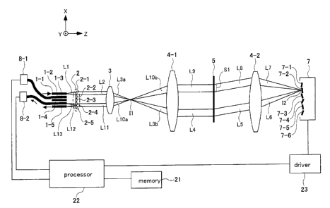
Fig. 1 is a schematic diagram of an attenuator device using
an offset-dispersion doublespectrograph accordingto one
embodiment of the invention.
As shown in the figure, the attenuator device of this
embodiment is configured to include: a plurality of
optical fibers 1-1 to 1-5; a micro lens array 2; a lens
3; lenses 4-1 and 4-2; a diffraction grating 5; a micro
mirror array 7; sensors 8-1 and 8-2; a driver 23 which
drives the micro mirror array 7; a processor 22 which gives
a command to the driver 23 in response to the outputs of
the sensor 8-1 and 8-2; and a memory 21 which stores various
programs and data to be used by the processor 22.
In Fig. l, the direction, in which a beam L2 to be spectrally
separated is incident on the channel attenuator device,
is set in the "Z direction", and the direction, which is
perpendicular to the Z direction and parallel to the
surface of the drawing, is set in the "X-direction".
Moreover, the direction perpendicular to the X-direction
and the Z-direction is set in the "Y-direction".
Therefore, the coordinate system shown in Fig. 1 is the
righthand system.
9
CA 02523555 2005-10-25
The optical fibers 1-1 to 1-5 are the members (e.g., the
single-mode fibers) , which introduce (as input ports) the
beam to be spectrally separated from the beam source (not
shown in the figure) into the channel attenuator device,
which guide ( as output ports ) the output beam of the channel
attenuator device to the outside, or which guide (as trap
ports) the output beam of the channel attenuator device
to the sensors 8-1 and 8-2. The beam emitting portions
of the optical fibers 1-1 to 1-5 have a diameter of 10
Vim, for example.
In this embodiment : the optical f fiber 1-1 is used as the
input port; the optical fibers 1-3 and 1-5 as the output
ports; and the optical fibers 1-2 and 1-4 as the trap ports .
Moreover, a beam source which is not shown in the figure
is arranged at the upstream stage of the optical fiber
1-1 to be used as the input port.
A mufti-wavelength beam Ll (having wavelength ranges of
~,1, ~,2, ..., and ?~6) emitted from the optical fiber 1-1
or the input port is collimated by a corresponding micro
lens 2-1 into the collimated beam L2.
The optical fibers 1-3 and 1-5 or the output ports are
arranged individually adjacently to the trap ports 1-2
and 1-4. Specifically, the trap port 1-2 and the output
port 1-3 make a pair, and the trap port 1-4 and the output
port 1-5 make a pair.
With the trap ports 1-2 and 1-4, there are connected the
CA 02523555 2005-10-25
sensors 8-1 and 8-2. These sensors 8-1 and 8-2 detect
the quantities of beams incident on the trap ports 1-2
and 1-4 and send the detection signals to the processor
22.
The micro lens array 2 includes a plurality of micro lenses
2-1 to 2-5, which are arranged to correspond to the optical
fibers 1-1 to 1-5, respectively. The micro lenses 2-1
to 2-5 have positive focal distances, which are optimized
for the NA (Numerical Aperture) of the optical fibers 1-1
to 1-5. Moreover, the micro lenses 2-1 to 2-5 are so
arranged that their own focal points may coincide with
the input/output portions of the optical fibers 1-1 to
1-5 corresponding thereto . As a result, the beam emitted
from the input port 1-1 is collimated by the corresponding
micro lens 2-1, and the collimated beams incident on the
micro lenses 2-2 to 2-5 enter the corresponding optical
f fibers ( i . a . , the output ports or the trap ports ) 1-2 to
1-5.
Now, the collimated beam L2 emitted from the micro lens
2-1 enters the lens 3 and becomes a converging beam L3a
so that it is focused as an intermediate image I1 at the
focal point of the lens 3. After having passed through
the focal point, the beam becomes a diverging beam L3b
and enters the lens 4-1 with an enlarged beam diameter .
The lens 4-1 is arranged to have the focused point of the
intermediate image I1 at the focal point . As a result,
11
CA 02523555 2005-10-25
a diverging beam L3 is collimated into a beam L4 by the
lens 4-1 . This collimated beam L4 enters the diffraction
grating 5. Here, the collimated beam L4 has the same
wavelength ranges of ~,1, ~.2, .. ., and ?~6 as those of the
mufti-wavelength beam L1.
The diffraction grating 5 focuses spectral images for the
individual wavelength ranges of 7~1, ~,2, ..., and ~,6 of
that incident beam at positions corresponding to the
diffraction angles of the wavelength ranges. Here, the
diffraction grating 5 is a transparent type planar
diffraction grating, in which amultiplicity of long slits
in the Y-direction are one-dimensionally arranged in
parallelwiththeX-direction. Inshort, thediffraction
grating 7 is arranged in symmetry with respect to the X-Z
plane . Here, the array direction of the multiple slits
corresponds to the wave dispersing direction of the
diffraction grating 5. In Fig. 1, only one optical path
of one of the wavelength ranges contained in the
mufti-wavelength beam L1 is displayed so as to facilitate
the grasp of the dispersion passage of a beam.
Now, the collimated beam L4 incident on the diffraction
grating 5 is dispersed, by the aforementioned wavelength
dispersing effect of the diffraction grating 5, at a
predetermined angle from the diffraction grating 5 in
accordance with the wavelength range. As a result, the
collimated beam L4 is diffracted by the diffraction
12
CA 02523555 2005-10-25
grating 5 into different angles for the individual
wavelength ranges so that it is converted into a diffracted
beam L5 having a different diffraction angle for each
wavelength range and incident on the lens 4-2.
Next, the diffracted beam L5, which has been diffracted
by the diffraction grating 5 into the different angle for
each of the wavelength ranges ( i . e. , ~,1, ~,2, . . . , and ~,6) ,
is condensed by the lens 4-2 as a converging beam L6 into
the micro mirror array 7. The beam thus condensed is
focused into an intermediate image T2 on the micro mirror
array 7. Here, the focused position of the intermediate
image I2 and the focused position of the intermediate image
I1 are located at conjugate positions in the optical system,
which is configured of the lens 4-1, the diffraction
grating 5 and the lens 4-2.
Here, the micro mirror array 7 is so arranged that the
converging beam L6 emitted from the lens 6 may be condensed
on the mirror surfaces of different micro mirrors 7-1 to
7-6 for the wavelength ranges, namely, that the converging
beam L6 in the wavelength range ~,l may be condensed on
the mirror surface of the micro mirror 7-1, that the
converging beam L6 in the wavelength range ~,2 may be
condensed on the mirror surface of the micro mirror 7-2,
and that the converging beam L6 in the wavelength range
~,6 may be condensed on the mirror surface of the micro
mirror 7-6.
13
CA 02523555 2005-10-25
The micro mirror array 7 is a device, in which the plural
micro mirrors 7-1 to 7-6 are arrayed along the X-axis
direction. This device is exemplified by the MEM5 (Micro
Electro Mechanical Systems) system. The plural micro
mirrors 7-1 to 7-6 have larger sizes than the spot diameter
(i.e., the diameter of the beam Ll to be spectrally
separated at the output portion of the input port 1-1)
of the intermediate image I2 of the converging beam L6.
The micro mirrors 7-1 to 7-6 have a size of about a square
of several 10 ~.m to several 100 Vim. Moreover, the
individual micro mirrors 7-1 to 7-6 can be independently
controlled at the inclination angles of the mirror
surfaces by drive signals coming from the driver 23.
In accordance with the command from the processor 22, the
driver 23 adjusts the individual inclination angles of
the micro mirrors 7-1 to 7-6 so that a reflected beam L7
of the converging beam L6 condensed into the micro mirrors
7-1 to 7-6maybe converted into a collimated beam L8 through
the lens 4-2 and may then reach a desired area S1 of the
diffraction grating 5.
Here, the position of the desired area Sl on the diffraction
grating 5 is predetermined according to the positions of
the pairs of the optical fibers 1-2 to 1-5 to be used as
the output ports and the trap ports. The processor 22
issuesthe commandsto controltheindividualinclination
angles of the micro mirrors 7-1 to 7-6 so that the reflected
14
CA 02523555 2005-10-25
beam L6 for each of the wavelength ranges (~,1, ~,2, . . . ,
and ~,6) from the micro mirrors 7-1 to 7-6 may reach the
area S1 which has been predetermined according to the
positions of the pairs of the optical fibers 1-2 to 1-5
to be used as the output ports and the trap ports.
Now, the collimated beam L8 having reached the desired
area Sl of the diffraction grating 5 is inversely
diffracted in the area S1 so that it goes as a
wavelength-multiplied collimated beam L9 into the lens
4-1. Here, the collimated beam L9 is parallel to the
collimated beam L4 to enter the diffraction grating 5.
Next, the collimated beam L9 goes into the lens 4-1 and
becomes a converging beam LlOb so that it is focused as
the intermediate image I1 at the focal point of the lens
4-1. After having passed through the focal point, the
beam is incident as the diverging beam LlOb on the lens
3 so that it is collimated into a collimated beam L11.
Next, the collimated beam L11 is converged by the micro
lenses 2-2 to 2-5 which are arranged to correspond to the
optical fibers 1-2 to 1-5 to be used as the output ports
and as the trap ports, so that they go into the beam
receiving portions of the output parts 1-3 and 1-5 and
the trap ports 1-2 and 1-4 located at the focal points
of the micro lenses 2-2 to 2-5.
In Fig. l, the pair of the output port 1-5 and the trap
port 1-4 is used as the output port and the trap port.
CA 02523555 2005-10-25
Moreover, a part of the collimated beam L11 is converged
by the micro lens 2-5 so that it goes as a converging beam
L12 into the beam receiving portion of the output port
1-5. On the other hand, the rest of the collimated beam
L11 is converged by the micro lens 2-4 so that it goes
as a converging beam L13 into the beam receiving portion
of the trap port 1-4.
The beam L13 thus introduced into the trap port 1-4 is
detected in its quantity by the sensor 8-2 so that the
detection signal is sent to the processor 22. The
processor 22 creates a command for controlling the
inclination angles of the micro mirrors 7-1 to 7-6 in the
directions so that the beam quantity indicated by the
detection signal from the sensor 8-2 may approach a set
value (i.e., information on the quantity of beam to be
discarded) stored in the memory 21, and outputs the command
to the driver 23. In response to the command, the driver
23 adjusts the inclination angles of the micro mirrors
7-1 to 7-6. In short, this embodiment makes a feedback
control for a predetermined attenuation.
Here will be detailed the attenuation actions of the
attenuator device according to this embodiment.
Fig. 2 presents enlarged diagrams of such a portion of
the attenuator device according to this embodiment as
includes the sensors 8-1 and 8-2, the optical fibers 1-1
to 1-5 and the micro lens array 2. Fig. 2 (A) shows the
16
CA 02523555 2005-10-25
optical path of the case, in which no attenuation is applied,
and Fig. 2 (B) and Fig. 2 (C) show optical paths of the case,
in which the attenuation is applied.
In the channel attenuator device according to this
embodiment, as has been described hereinbefore, the
inclination angles of the micro mirrors 7-1 to 7-6 are
adjusted to introduce a part ( i . a . , the converging beam
L13) of the collimated beam L11 emitted from the lens 3
into the trap port 1-4 and the output port 1-5 thereby
to attenuate the quantity of the converging beam L12 to
be output to the outside.
In the absence of the attenuation, as shown in Fig. 2 (A) ,
the collimated beam L11, which is emitted from the lens
3 by the beam L1 to be spectrally separated, as incident
from the optical fiber 1-1, is introduced only into an
area S2, i . a . , the micro lens 2-5 by the controls of the
reflection angles of the micro mirrors 7-1 to 7-6 by the
driver 23. Therefore, the collimated beam L11 does not
receive the attenuation but becomes the converging beam
L12 so that it is input to the output port 1-5 and output
to the outside.
In the presence of the attenuation, as shown in Fig. 2 (B) ,
the collimated beam L11, which is emitted from the lens
3 by the beam L1 to be spectrally separated, as incident
from the optical fiber 1-1, is introduced into an area
S3 positioned positively farther in the X-direction than
1 '7
CA 02523555 2005-10-25
the area S2, namely, a part is input to the micro lens
2-4 whereas the rest is input to the micro lens 2-5 by
the controls of the reflection angles of the micro mirrors
7-1 to 7-6 by the driver 23. Therefore, the collimated
beam L11 becomes the attenuated converging beam L12 so
that it is input to the output port 1-5 and output to the
outside. On the other hand, the part of the collimated
beam L11 to be discarded is introduced as the converging
beam L13 into the trap port 1-4 so that the beam quantity
is detected by the sensor 8-2.
On the other hand, as shown in Fig. 2 (C) , the collimated
beam L11, which is emitted from the lens 3 by the beam
L1 to be spectrally separated, as incident from the optical
fiber 1-1, is introduced into an area S4 positioned
positively farther in the X-direction than the area S3,
namely, the incidence can be made only on the micro lens
2-4 by the controls of the reflection angles of the micro
mirrors 7-1 to 7-6 by the driver 23. In this case, the
collimated beam L11 is not output from the output port
1-5 to the outside. The collimated beam L11 is input
entirely as the converging beam L13 to the trap port 1-4,
and its quantity is detected by the sensor 8-2.
In this embodiment, the beam L13, as introduced into the
trap port 1-4, is detected in its quantity by the sensor
8-2, and its detection signal is sent to the processor
22. This processor 22 creates the command to control the
18
CA 02523555 2005-10-25
inclination angles of the micro mirrors 7-1 to 7-6 to the
direction, in which the beam quantity indicated by the
detection signal from the sensor 8-2 approaches the set
value ( i . a . , the information on the quantity of the beam
to be discarded) stored in the memory 21, and outputs the
command to the driver 23. In response to this command,
the driver 23 adjusts the inclination angles of the micro
mirrors 7-1 to 7-6.
One embodiment of the invention has been described
hereinbefore.
In this embodiment the output ports and the trap ports
are arranged adj acently to each other, and the inclination
angles of the micro mirrors 7-1 to 7-6 are controlled,
whereby of the collimated beam L11 output from the lens
3, the ratio can be adjusted between the converging beam
L12 to be emitted to the output ports and the converging
beam L13 to be output to the trap ports . Unlike the channel
attenuator device described in the aforementioned Patent
Document l, therefore, the micro mirror array need not
be so configured that the diameters of the individual micro
mirrors are smaller than the spot diameters of the beams
(to be operated) to enter the micro mirror array, and that
the multiple micro mirrors are arranged in the spot
diameters of the beams to be operated. It is, therefore,
possible to provide an attenuator device having a simpler
configuration. Moreover, the quantityof beam discarded
19
CA 02523555 2005-10-25
can be monitored with the simple configuration, in which
the trap ports are arranged adj acently to the output ports .
Here, the present invention should not be limited to the
embodiment thus far described but can be modified in
various manners within the scope of the gist thereof . For
example, the transparent type planar diffraction grating
is used as the diffraction grating 5 in the above-described
embodiment but may be modified into a reflection type
planar diffraction grating, for example. In this
modification, the lenses 4-1 and 4-2 can also be configured
of one Lens.
In this embodiment, moreover, the inclination angles of
the micro mirrors 7-1 to 7-6 may also be so controlled
that the diffracted beams may be output to the desired
pair of the output port and the trap port for the individual
wavelength ranges ( i . a . , ~,1, ~,2, . . . , and ~,6 ) diffracted
by the diffraction grating 5.
In this embodiment, moreover, the inclination angles of
the micro mirrors 7-1 to 7-6 may also be controlled to
adjust the ratio between the converging beam L12 to be
emitted to the output port and the converging beam L13
to be output to the trap port, for the individual wavelength
ranges (i . a . , ~,1, ~,2, . . . , and ~.6) diffracted by the
diffraction grating 5.
Moreover, the present invention has been described on
the embodiment, in which it is used in the
CA 02523555 2005-10-25
offset-dispersion double spectrograph, but can also be
applied to an optical cross connector or a switching
element or the like. Here, there is nothing to say that
the embodiment is the attenuator device but may also be
an optical switching device, which switches the output
destination of a beam from an input port. The embodiment
can also be applied to another widely used spectroscope.
Moreover, the embodiment can be used in the optical path
reversed from the embodied one, too . In short, the present
invention can also be used such that a beam is input from
a plurality of input ports and output from a single output
port.
21