Note: Descriptions are shown in the official language in which they were submitted.
CA 02523747 2005-10-24
WO 2004/102739 PCT/GB2004/002016
1
Phased Array Antenna System with Adjustable Electrical Tilt
The present invention relates to ' a phased array antenna system with
adjustable electrical tilt. It is suitable for use in many areas of
telecommunications but finds particular application in cellular mobile radio
networks, commonly referred to as mobile telephone networks. More
specifically, but without limitation, the antenna system of the invention may
be used with second generation (2G) mobile telephone networks such as the
GSM system, and third generation (3 G) mobile telephone networks such as
the Universal Mobile Telephone System (UMTS).
Operators of cellular mobile radio networks generally employ their own
base-stations, each of which has at least one antenna. In a cellular mobile
radio network, the antennas are a primary factor in defining a coverage area
in which communication to the base station can take place. The coverage
area is generally divided into a number of overlapping cells, each associated
with a respective antenna and base station. The cells are also generally
divided into sectors to increase the communications coverage.
The antenna of each sector is connected to a base . station for radio
communication with all of the mobile radios in that sector. Base stations are
interconnected by other means of communication, usually point-to-point
radio links or fixed land-lines, allowing mobile radios throughout the cell
coverage area to communicate with each other as well as with the public
telephone network outside the cellular mobile radio network.
Cellular mobile radio networks which use phased array antennas are known:
such an antenna comprises an array (usually eight or more) individual
CA 02523747 2005-10-24
WO 2004/102739 PCT/GB2004/002016
2
antenna elements such as dipoles or patches. The antenna has a radiation
pattern consisting of a main lobe and sidelobes. The centre of the main lobe
is the antenna's direction of maximum sensitivity, i.e. the direction of its
main radiation beam. It is a well known property of a phased array antenna
that if signals received by antenna elements are delayed by a delay which
varies linearly with distance from an edge of the array, then the antenna main
radiation beam is steered towards the direction of increasing delay. The
angle between main radiation beam centres corresponding to zero and non
zero variation in delay, i.e. the angle of steer, depends on the rate of
change
of delay with distance across the array.
Delay may be implemented equivalently by changing signal phase, hence the
expression phased array. The main beam of the antenna pattenl can therefore
be altered by adjusting the phase relationship between signals fed to
different
antenna elements. This allows the beam to be steered to modify the coverage
area of the antenna.
Operators of phased array antennas in cellular mobile radio networks have a
requirement to adjust their antennas' vertical radiation pattern, i.e. the
pattern's cross-section in the vertical plane. This is necessary to alter the
vertical angle of the antenna's main beam, also known as the "tilt", in order
to adjust the coverage area of the antenna. Such adjustment may be required,
for example, to compensate for change in cellular network structure or
number of base stations or antennas. Adjustment of antenna angle of tilt is
known both mechanically and electrically, and both individually or in
combination.
CA 02523747 2005-10-24
WO 2004/102739 PCT/GB2004/002016
3
Antenna angle of tilt may be adjusted mechanically by moving antenna
elements or their housing (radome): it is referred to as adjusting the angle
of
"mechanical tilt". As described earlier, antenna angle of tilt may be adjusted
electrically by changing time delay ~r phase of signals fed to or received
from each antenna array element (or group of elements) without physical
movement: this is referred to as adjusting the angle of "electrical tilt".
When used in a cellular mobile radio network, a phased array antenna's
vertical radiation pattern (VRP) has a number of significant requirements:
1. high main lobe (or boresight) gain;
2. a first upper side lobe level sufficiently low to avoid interference
to mobiles using a base station in a different cell or network;
3. a first lower side lobe level sufficiently high to allow
communications in the immediate vicinity of the antenna.
These requirements are mutually conflicting: for example, increasing the
boresight gain may increase the level of the side lobes. A first upper side
lobe level, relative to the boresight level, of -1 ~dB has been found to
provide
a convenient compromise in overall system performance.
The effect of adjusting either the angle of mechanical tilt or the angle of
electrical tilt is to reposition the boresight so that it points either:
above' or
below the horizontal plane, which changes the coverage area of the antenna.
It is desirable to be able to vary both the mechanical tilt and the electrical
tilt
of an antenna of a cellular radio base station: this allows maximum
flexibility in optimisation of cell or sector coverage, since these forms of
tilt
have different effects on antenna ground coverage and also on other antennas
CA 02523747 2005-10-24
WO 2004/102739 PCT/GB2004/002016
4
in the station's immediate vicinity. Moreover, operational efficiency is
improved if the angle of electrical tilt can be adjusted remotely from the
antenna assembly. Whereas an antenna's angle of mechanical tilt may be
adjusted by repositioning its radome, changing its angle of electrical tilt ,
requires additional electronic circuitry which increases antenna cost and
complexity. Moreover, if a single antenna is shared between a number of
operators, it is preferable to provide an individual angle of electrical tilt
for
each operator.
The need for an individual angle of electrical tilt from a shared antenna has
hitherto not been met and has resulted in compromises in system
performance. Further reductions in system performance may also occur if the
gain decreases as a consequence of the technique adopted to change the
angle of electrical tilt.
R. C. Johnson, Antenna Engineers Handbook, 3rd Ed 1993, McGraw Hill,
ISBN 0 - 07 - 032381 - X, Ch 20, Figure 20-2 discloses a method for locally
or remotely adjusting the angle of electrical tilt of a phased array antenna.
In
this method, a radio frequency (RF) transmitter carrier signal is fed to the
antenna and distributed to the antenna's radiating elements. Each antenna
element has a variable phase shifter associated with it so that signal phase
. can be. adjusted as a function of distance across the antenna to vary the
antenna's angle of electrical tilt. The distribution of power when not tilted
is
proportioned so as to set the. side lobe level and boresight gain. ~ptimum
control of the angle of tilt is obtained when the phase front is controlled
fox
all angles of tilt so that the side lobe level is not increased over the tilt
range.
The angle of electrical tilt can be adjusted remotely, if required, by using a
servo-mechanism to control the position of the phase shifters.
CA 02523747 2005-10-24
WO 2004/102739 PCT/GB2004/002016
This prior art method antenna has a number of disadvantages. A variable
phase shifter is required for every antenna element. The cost of the antenna
is high due to the number of such phase shifters required. Cost may be
reduced by using a single common delay device or phase shifter for a group
5 of antenna elements instead of per element, but this increases the side lobe
level. See for example published International Patent Application No.
WO 03/036756 A2 and Japanese Patent Application No. JP20011211025 A.
Mechanical coupling of delay devices may be used to adjust delays, but it is
difficult to do this correctly; moreover, mechanical links and gears result in
non-optimum distribution of delays. The upper side lobe level increases
when the antenna is tilted downwards, thus causing a potential source of
interference to mobiles using other base stations. If the antenna is shared by
a number of operators, the operators then have a common angle of electrical
tilt instead of different ~ angles which is preferable. Finally, if the
antenna is
used in a communications system having up-link and down-link at different
frequencies (frequency division duplex system), the angle of electrical tilt
in
transmit mode is different from that in receive mode because of frequency
dependence of properties of signal processing components.
International Patent Application Nos. PCT/GB2002/004166 and
PCT/GB2002/004930 describe locally or remotely adjusting an antenna's
angle of electrical tilt by means of a difference in phase between a pair of
signal feeds connected to the antenna.
It is an object of the present invention to provide an alternative form of
phased array antenna system.
CA 02523747 2005-10-24
WO 2004/102739 PCT/GB2004/002016
6
The present invention provides a phased array antenna system with
adjustable electrical tilt and comprising an array of antenna elements
characterised in that the system incorporates:
a) a variable phase shifter for introducing a variable relative phase shift
between first and second RF signals,
b) splitting apparatus for dividing the relatively phase shifted first and
second signals into component signals, and
c) a signal combining network for forming vectorial combinations of the
component signals to provide a respective drive signal for each individual
antenna element with appropriate phasing relative to other drive signals
such that the angle of electrical tilt of the array is adjustable in response
to alteration of the variable relative phase shift introduced by the variable
phase shifter.
The invention provides the advantage that it is possible to adjust electrical
tilt for the whole array using only a single variable phase shifter, instead
of
one variable phase shifter per antenna element or group of antenna elements
as in the prior art. If one or more additional phase shifters are used, an
extended range of electrical tilt can be obtained.
The antenna system may have an odd number of antenna elements. The
variable phase shifter may be a first variable phase shifter, the system
including a second variable phase shifter arranged to phase shift a
c~mponent signal which has been phase shifted by the first variable phase
shifter, and the second variable phase shifter providing a further component
signal output for the signal combining arid phase shifting network either
directly or via one or more splitter/variable phase shifter combinations.
CA 02523747 2005-10-24
WO 2004/102739 PCT/GB2004/002016
7
The variable phase shifter may be one of a plurality of variable phase
shifters, the signal phase shifting and combining network being arranged to
produce antenna element drive signals from component signals some of
which have passed through all the variable phase shifters and some of which
have not.
The splitting apparatus may be arranged to divide a component signal into
further component signals for input to the signal phase shifting and
combining network. The signal phase shifting and combining network may
employ phase shifters and hybrid couplers (hybrids) for phase shifting and
vectorially combining the component signals. The hybrids may , be 1 ~0
degree hybrids, also known as sum-and-difference hybrids. The hybrids may
be constructed as ring hybrids each with circumference (n+1/~,)~, and input
and output ports separated by 7~/4, where n is an integer and ~, is the
wavelength of the RF signals in material of which each ring hybrid is
constructed. The input and output ports of each hybrid are matched to the
system impedance.
The hybrids for vectorially combining the component signals may be
designed to convert input signals I1 and I2 into vector sums and differences
other than (I1+ I2) and (I1- I2).
The splitting apparatus, variable phase shifter, and the signal phase shifting
and combining network may be co-located with the antenna array to form an
antenna assembly, the assembly having a single RF input power feeder from
a remote source. Alternatively, the splitting apparatus may incorporate first,
,second and third splitters, the first splitter being located with the
variable
phase shifter remotely from the second and third splitters, the second and
CA 02523747 2005-10-24
WO 2004/102739 PCT/GB2004/002016
8
third sputters, the signal phase shifting and combining network and the
antenna array being co-located as an antenna assembly, and the assembly
having dual RF input power feeders from a remote source at which the first
sputter and variable phase shifter are located.
The variable phase shifter may be a first variable phase shifter connected in
a
transmit channel, the system including a second variable phase shifter
connected in a receive channel: there may be similar transmit and receive
channels providing fixed phase shifts instead of variable phase shift: the
signal phase shifting and combining network is then arranged to operate in
both transmit and receive modes by producing antenna element drive signals
in response to signals in the tt~ansmit channels and producing a receive
channel signal from signals developed by antenna elements operating in
receive mode. The angle of electrical tilt is then independently adjustable in
each mode.
The variable phase shifter may be one of a plurality of variable phase
shifters
associated with respective operators, and the system includes filtering and
combining apparatus for routing signals on to common signal feed apparatus
after phase shifting in respective variable phase shifters, the common signal
feed apparatus being connected to splitting apparatus and a signal combining
and phase shifting network for providing signals to the antenna containing
contributions from both operators with independently adjustable electrical
tilt. The plurality of variable phase shifters may comprise a respective pair
of
variable phase shifters ' associated with each operator, and the system may
have components which have both ,forwaxd and reverse signal processing
capabilities such that the system is operative in transmit and receive modes
with independently adjustable electrical tilt in each mode.
CA 02523747 2005-10-24
WO 2004/102739 PCT/GB2004/002016
9
In another aspect, the present invention provides a method of adjusting the
electrical tilt of a phased array antenna. system, the system including an
array
of antenna elements, characterised in that the method incorporates:
a) introducing a variable relative phase shift between first and second l~F
signals,
b) dividing the relatively phase shifted first and second signals into
component signals, and
c) vectorially combining and relatively phase shifting the component signals
to provide to provide a respective drive signal for each individual antenna
element with appropriate phasing relative to other drive signals such that
the angle of electrical tilt of the array is adjustable in response to
alteration of the variable relative phase shift.
The array may have an odd number of antenna elements.
The method may include generating at least one component signal which
has undergone phase shifting in a plurality of variable phase shifters. The
variable phase shifters may be ganged, the method including producing
antenna element drive signals from component signals some of which have
passed through all the variable phase shifters and some of which have not.
The method may include dividing a component signal into further
component signals for input to the signal phase shifting and combining
network. It may employ phase shifters and hybrids for phase shifting and
vectorially combining the component signals. The hybrids may be 180
degree hybrids. They may be ring hybrids with circumference (n+1/2)7 and
input and output ports separated by 7~/4, where n is an integer and 7~ is the
wavelength of the RF signals in material of which each ring hybrid is
CA 02523747 2005-10-24
WO 2004/102739 PCT/GB2004/002016
constructed. The splitting apparatus may also incorporate such ring hybrids,
one port of each hybrid being terminated in a resistor equal in value to the
system impedance to form a matched Ioad.
The hybrids for vectorially combining the component signals may be
5 designed to convert input signals I1 and I2 into vector sums and differences
other than (I1+I2) and (I1-I2). o
The method may include feeding a single RF input signal from a remote
source for splitting, variable phase shifting and vectorial combining in a
network co-located with the antenna array to form an antenna assembly. It
10 may alternatively include feeding two RF input signals with variable phase
relative to one another from a remote source to an antenna assembly and
splitting, phase shifting and combining signals in a network co-located with
the antenna array. It may employ transmit and receive channels for operation
in both transmit and receive modes, producing antenna element drive signals
in response to a signal in the transmit channels and producing a receive
channel signal from signals developed by antenna elements operating in
receive mode.
The variable phase shifter may be one of a plurality of variable phase
shifters
associated~with respective operators, and the method may include:
a) filtering and combining signals and passing them to common signal feed
apparatus after phase shifting in respective variable phase shifters, the
common signal feed apparatus being connected to the splitting apparatus
and the signal combining and phase shifting network;
b) providing signals to the antenna containing contributions from both
operators; and
CA 02523747 2006-09-12
29756-303(S)
11
c) independently adjusting electrical tilt
associated with each operator.
The plurality of variable phase shifters may
comprise a respective pair of variable phase shifters
associated with each operator; the method may employ
components which have both forward and reverse signal
processing capabilities, and the method may include
operating in transmit and receive modes with independently
adjustable electrical tilt in each mode.
I0 In still another aspect the present invention
provides a phased array antenna system with adjustable
electrical tilt and comprising an array of antenna elements,
the system incorporating: a) a variable phase shifter for
introducing a variable relative phase shift between first
and second RF signals, b) splitting apparatus for dividing
the first RF signals into first component signals and the
second RF signals into second component signals, and c) a
signal combining network for forming vectorial combinations
of first component signals with second component signals,
the splitting apparatus and the signal combining network
being in combination a means for providing drive signals for
individual antenna elements, the drive signals varying in
phase in accordance with a substantially linear function of
antenna element position in the array as required for normal
phased array operation and the angle of electrical tilt of
the array being adjustable in response to alteration of the
variable relative phase shift introduced by the variable
phase shifter.
In yet another aspect the present invention
provides a method of adjusting the electrical tilt of a
phased array antenna system, the system including an array
of antenna elements, and the method incorporating:
CA 02523747 2006-09-12
29756-303(S)
11a
a) introducing a variable relative phase shift between first
and second RF signals, b) dividing the first RF signals into
first component signals and the second RF signals into
second component signals and vectorially combining the first
component signals with the second component signals to
provide drive signals for individual antenna elements, the
drive signals varying in phase in accordance with a
substantially linear function of antenna element position in
the array as required for normal phased array operation and
the angle of electrical tilt of the array being adjustable
in response to alteration of the variable relative phase
shift.
In order that the invention might be more fully
understood, embodiments thereof will now be described, by
way of example only, with reference to the accompanying
drawings, in which:-
Figure 1 shows a vertical radiation pattern (VRP)
of a phased array antenna with zero and non-zero angles of
electrical tilt;
Figure 2 illustrates a prior art phased array
antenna having an adjustable angle of electrical tilt;
Figure 3 is a block diagram of a phased array
antenna system of the invention;
Figure 4 shows in more detail a signal combining
network used in the Figure 3 system;
Figure 5 is a phase diagram of antenna element
signals associated with a ninety degree phase shift
introduced by a variable phase shifter in the Figure 3
system;
CA 02523747 2006-09-12
29756-303 (S)
11b
Figures 6 and 7 are block diagrams of parts of
further phased array antenna systems of the invention
incorporating eleven and twelve antenna
CA 02523747 2005-10-24
WO 2004/102739 PCT/GB2004/002016
12
elements respectively (element spacing is not wholly to scale in
Figure 6);
Figure ~ is a phase diagram of antenna element signals associated with a
ninety degree phase shift introduced by a.variable phase shifter in
the Figure 7 system;
Figure 9 is a block diagram of part of another phased array antenna system
of the invention employing two variable phase shifters;
Figure 10 is a block diagram of part of an antenna system of the invention
similar to that shown in. Figure 9 but employing ganged variable
phase shifters;
Figures 11 and 12 illustrate use of the invention with single and dual feeders
respectively;
Figure 13 shows a modification to the invention allowing angles of
electrical, tilt in transmit mode and receive mode to be
independently adjustable;
Figure 14 is a block diagrafn of another phased array antenna system of the
invention illustrating antenna sharing by multiple users with dual
feeders and individual tilt and transmit/receive capability;
Figure 15 is a variant of the antenna system of Figure 9 with variable phase
shifters located remotely from one another; and
Figure 16 illustrates a phased array antenna system of the invention
incorporating ring hybrid couplers.
CA 02523747 2005-10-24
WO 2004/102739 PCT/GB2004/002016
13
All examples illustrated employ connections for which source impedances of
signals axe equal to respective load impedances in order to form a 'matched'
system. A matched system maximises the power transmitted from a source to
a load and avoids signal reflections. Where signal lines are terminated in a
resistor (see e.g. Figure 6) the value of the resistor is equal to the system
impedance in order to form a matched termination.
Referring to Figure 1, there axe shown vertical radiation patterns (VRP) 10a
and 10b of an antenna 12 which is a phased array of individual antenna
elements (not shown). The antenna 12 is planar, has a centre 14 and extends
vertically in the plane of the drawing. The VRPs 10a and 10b correspond
respectively to zero and non-zero variation in delay or phase of antenna
element signals with distance across the antenna 12. They have respective
main lobes 16a, 16b with centre lines or "boresights" 18a, 18b, first upper
sidelobes 20a, 20b and first lower sidelobes 22a, 22b; 18c indicates the
boresight direction for zero variation in delay for comparison with the non-
zero equivalent 18b~. When referred to without the suffix a or b, ~e.g.
sidelobe
20, either of the relevant pair of elements is being referred to without
distinction. The VRP 10b is tilted (downwards as illustrated) relative to
VRP 10a, i.e. there is an angle - the angle of tilt - between main beam centre
lines 18b and 18c which has a magnitude dependent on the rate at which
delay varies with distance across the antenna 12.
The VRP has to satisfy a number of criteria: a) high boresight gain; b) the
first upper side lobe 20 should be at a level low enough to avoid causing
interference to mobiles using another cell and c) the first lower side lobe 22
should be sufficient for communications to be possible ' in the antenna's
immediately vicinity.
CA 02523747 2005-10-24
WO 2004/102739 PCT/GB2004/002016
14
The requirements are mutually conflicting: for example, maximising
boresight gain may increase side lobes 20, 22. Relative to a boresight level
(length of main beam 16), a first upper side lobe level of -l~d~ has been
found to provide a convenient compromise in overall system performance.
Foresight gain decreases in proportion to the cosine of the angle of tilt due
to
reduction in the antenna's effective aperture. Further reductions in boresight
gain may result depending on how the angle of tilt is changed.
The effect of adjusting either the angle of mechanical tilt or the angle of
electrical tilt is to reposition the boresight so that it points either above
or
below the horizontal plane, and hence increases or decreases the coverage
area of the antenna. For maximum flexibility of use, a cellular radio base
station preferably has available both mechanical tilt and electrical tilt
since
each has a different effect on the shape and area of ground coverage and also
on other antennas both in the immediate vicinity and in neighbouring cells.
It is also convenient if an antenna's electrical tilt can be adjusted remotely
from the antenna. Furthermore, if a single antenna is shared between a
number of operators it is preferable to provide an individual angle of
electrical tilt for each operator.
Referring now to Figure 2, a prior art phased array antenna system 30 is
shown in which the angle of electrical tilt is adjustable. The system 30
incorporates an input 32 for a radio frequency (RF) transmitter carrier
signal,
the input being connected to a power distribution network 34. The network
34 is connected via phase shifters Phi.EO, Phi.ElL to Phi.E[n]L and Phi.ElU
to Phi.E[n]U to respective radiating antenna elements E0, E1L to E[n]L and
ElU to E[n]U respectively of the phased array antenna system 30: here
suffixes U and L indicate upper and lower respectively, n is an arbitrary
CA 02523747 2005-10-24
WO 2004/102739 PCT/GB2004/002016
positive integer greater than 2 which defines phased at~ray size, and dotted
lines such as 3~ indicating the relevant element may be replicated as required
for any desired array size.
The phased array antenna system 30 operates as follows. An RF transmitter
5 carrier signal is fed via the input 32 to the power distribution network 34:
the
network 34 divides this signal (not necessarily equally) between the phase
shifters Phi.EO, Phi.ElL to Phi.E[n]L and Phi.ElU ~ to Phi.E[n]U, which
phase shift the signals they receive and pass on the resulting phase shifted
signals to respective associated antenna elements E0, E1L to E[n]L, E1U to
10 E[n]U. The phase shifts and signal amplitudes to each element are chosen to
select an appropriate angle of electrical tilt. The distribution of power by
the
network 34 when the angle of tilt is zero is chosen to set the side lobe level
and boresight gain appropriately. Optimum control of the angle of tilt is
obtained when the phase front is controlled for all angles of tilt so that the
15 side lobe level is not increased significantly over the tilt range. The
angle of
electrical tilt can be adjusted remotely, if required, by using a servo-
mechanism to control the phase shifters Phi.EO, Phi.EIL to Phi.E[n]L and
Phi.ElU to Phi.E[n]U, which may be mechanically actuated.
The prior art phased array antenna system 30 has a number of disadvantages
20 as follows:
a) a respective phase shifter is required for each antenna element, or per
group of elements;
b) the cost of the antenna is high due to the number of phase shifters
required;
CA 02523747 2005-10-24
WO 2004/102739 PCT/GB2004/002016
16
c) cost reduction by applying phase shifters to groups of elements
increases the side lobe level;
d) mechanical coupling of the phase shifters to set delays correctly is
difficult and mechanical links and gears are used which result in a non
optimum delay scheme;
e) the upper side lobe level increases when the antenna is tilted
downwards causing a potential source of interference to mobiles using
other cells ;
f) if an antenna is shared by different operators, all must use the same
angle of electrical tilt;
g) in a. system with up-link and down-link at different frequencies
(frequency division duplex system), the angle of electrical tilt in
transmit is different from that'in receive;
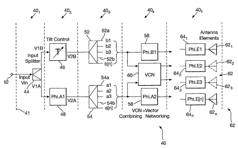
Referring now to Figure 3, a phased array antenna system 40 of the invention
is shown which has an adjustable angle of electrical tilt. The system 40
incorporates five successive functional regions 401 to 405 referred to in the
art as "levels" and indicated between pairs of dotted lines such as 41. It has
an input 42 for an RF carrier transmission signal: the input 42 is connected
as input to a power sputter 44 providing two output signals having
amplitudes V1A, V1B, these becoming input signals to a variable phase
shifter 46 and a first fixed phase shifter 4~ respectively. The phase shifters
46 and 4~ may equivalently be considered as time delays. They provide
respective output signals V2B and V2A to two power splatters 52 and 54
respectively. The power splatters 52 and 54 have n outputs such as 52a and
54a respectively: here n is a positive integer equal to 2 or more, and dotted
CA 02523747 2005-10-24
WO 2004/102739 PCT/GB2004/002016
17
outputs 52b and 54b indicate the output in each case may be replicated as
required for any desired phased axray size.
The power splitter outputs such as 52a and 54a provide output signals having
amplitudes Va1 to Va[n] and Vb1 to Vb[n] respectively (illustrated without
the letter V). As will be described later in more detail, some of these output
signals may have amplitudes equal to others and some unequal. In one
embodiment (to be described) having ten antenna elements (n - 5),
Va1 = Va2 = Va3, Vb3 = Vb4 = VbS; Va4 = Vb2 and Va5 = Vbl. These
output signals are fed to the phase shifting and combining level 404, which
contains second and third fixed phase shifters 56 and 58 and vector
combining networl~s indicated collectively by 60. The level 404 will be
described in more detail later: it provides drive signals to equispaced
antenna
elements 621 to 62n of a phased array 62 via respective fixed phase shifters
641 to 64n. Here as before n is an arbitrary positive integer equal to or
greater
than 2 but equal to the value of n for the power splitters 52 and 54, and
phased array size is 2n antenna elements. Inner antenna elements 622 and 623
are shown dotted to indicate they may be replicated as required for any
desired phased array size.
The phased array antenna system 40 operates as follows. An RF transmitter
carrier signal is fed (single feeder) via the input 42 to the power splitter
44
where it is divided into signals V1A and V1B (of equal power in this
example). The signals V 1A and V 1B are fed to the variable and fixed phase
shifters 46 and 48 respectively. The variable phase shifter 46 applies an
operator-selectable phase shift or time delay, and the degree of phase shift
applied here controls the angle of electrical tilt of the entire phased array
62
of antenna elements 621 etc. The fixed phase shifter 48 is not essential but
CA 02523747 2005-10-24
WO 2004/102739 PCT/GB2004/002016
18
convenient: it applies a fixed phase shift which for convenience is chosen to
be half the imun~ phase shift ~M applicable by the variable phase shifter
46. This allows V1A to be variable in phase in the range -c~M/2 to +c~M/2
relative to V1B, and these signals after phase shift become V2B and V2A as
has been said after output from the phase shifters 46 and 48.
Each of the power splitters 52 and 54 divides signals V2B or V2A into a
respective set of n output signals Vb1 to Vb[n] or Va1 to Va[n], where the
power of each signal in each set Vb1 etc. or Va1 etc. is not necessarily equal
to the powers of the other signals in its set. The variation of signal powers
across the sets Va1 etc. and VbI etc. is different for different numbexs of
antenna elements 621 etc. in the array 62.
One of the set of output signals Vbl to Vb[n] is fed to a respective fixed
antenna phase shifter 643 via the second phase shifter 56, and one of the set
of output signals Va1 to Va[n] is likewise fed to another antenna phase
shifter 64g via the third phase shifter 58. The second and third phase
shifters
56 and 58 introduce padding phase shifts to compensate for that introduced
by the combining networks 60. Other signals in the sets Vb 1 to Vb [n] and
Va1 to Va[n] are combined in pairs in the networks 60 to produce vectorially
added resultant signals for driving respective antenna elements 621 etc via
phase shifters 641 etc. The fixed phase shifters 641 etc. impose fixed phase
shifts which vary between different antenna elements 621 etc. according to
element geometrical position across the array 62: this sets a zero reference
direction (18a or I8b in Figure 1) for the array 62 boresight when zero phase
difference between the signals VIA and V1B imposed by the variable phase
shifter 46.. The antenna phase shifters 641 etc.~ are not essential, but they
are
preferred because they can be used to a) proportion correctly the phase shift
CA 02523747 2005-10-24
WO 2004/102739 PCT/GB2004/002016
19
introduced by the tilt process, b) optimise suppression of the side lobes over
the tilt range, and c) introduce an optional fixed angle of electrical tilt.
The angle of electrical tilt of the array 60 is variable simply by using one
variable phase shifter, the variable phase shifter 46. This compares with the
prior art requirement to have multiple variable phase shifters, one for every
antenna element or sub-group of antenna elements. When the phase
difference introduced by the variable phase shifter 46 is positive relative to
the fixed phase shift 48 the antenna tilts in one direction, and when that
phase difference is negative the antenna tilts in the opposite direction.
If there are a number of users, each user may have a respective phased array
antenna system 40. Alternatively, if it is required that users share a common
antenna , while retaining an individual electrical tilt capability, then each
user may have a respective set of levels 401 and 402 in Figure 3. In addition,
a combining network consisting of levels 403, , 404 and 405 is required to
combine signals from the resulting plurality of sets of sputters 44 and phase
shifters or delays 46 and 48 for feeding to the antenna array 62. Published
International Patent Application No. WO 03/043127 A3 describes sharing in
this way, but ' it uses an antenna with multiple sub-groups of antenna
elements, each antenna element in a sub-group having the same element
drive signal phase. In the antenna system 40, the antenna elements 621 to 62n
all have different element drive signal phases as required for improved
phased array performance.
It can be shown that the antenna system 40 has good side lobe suppression
that is maintained over its electrical tilt range. The antenna system 40 can
be
implemented at lower cost than contemporary designs offering a similar
CA 02523747 2005-10-24
WO 2004/102739 PCT/GB2004/002016
level of performance. Its electrical tilt may be adjusted remotely using a
single variable delay device, and this permits different operators to share it
while providing each operator with an individual angle of electrical tilt. The
angle of electrical tilt in transmit mode may either be the same, or different
5 from that in receive mode by modifying the antenna system 40 to include
different paths and phase shifters for transmit and receive as will be
described later.
Referring now to Figure 4, there is shown part of an implementation 70 of
. the invention for a phased array 62 of ten elements 621 to 6210. Parts
10 equivalent to those previously described are like referenced. Figure 4
corresponds to parts 403 to 405 of Figure 3; and splatters 52 and 54 are shown
exchanged in position. The splatters 52 and 54 receive respectively input
signals V2B and V2A of equal power but variable relative phase. They each
split their respective inputs into five signals, three of which are of the
same
15 amplitude (A or B), and the other two are 0.32 and 0.73 of that amplitude
(0.32 or 0.73 of A or B).
Eight of the ten signals from the sputters 52 and 54 pass to four vector
combining devices 601 to 60ø: each of these devices is a 180 degree hybrid
(marked H) having two input terminals designated I1 and I2 and two output
20 terminals designated S and D for sum and difference respectively. The
references I1 and I2 will also be used for convenience to indicate signals at
those terminals. As indicated by the terminal designations, on receipt of
input signals I1 and I2, each of the hybrids 601 to 604 produces two output
signals at S and D which are the vector sum and difference of its respective
input signals. Table 1 below shows the input signal amplitudes received by
CA 02523747 2005-10-24
WO 2004/102739 PCT/GB2004/002016
21
the hybrids 601 to 604 and the output signals in vector form generated in
response, expressed in terns of arbitrary values A and B in sash case.
Table 1
Hybrid I1 Input I2 Input S ~utput 17 ~utput
601 A 0.738 0.707(A + 0.73B)0.707(A - 0.73B)-
602 ' A 0.32B 0.707(A + 0.32B)0.707(A - 0.32B)
603 B . 0.32A 0.707(B + 0.32A)0.707(B - 0.32A)
604 B 0.73A 0.707(B + 0.73A)0:707(B - 0.73A)
Table 2 below shows the antenna elements which receive the output signals
generated by the splatters 52 and 54 and hybrids 601 to 604 via antenna phase
shifters (PS) 641 to 6410.
Table 2
Antenna Signal Antenna Signal
Element Amplitude Element Amplitude
621 0.707(B - 0.73A) 626 0.707(A + 0.73B)
622 0.707(B - 0.32A) 627 0.707(A + 0.32B)
623 B 628 A
624 , 0.707(B + 0.32 629 0.707(A - 0.328)
A)
625 0.707(B + 0.73A) 6210 0.707(A - 0.738)
CA 02523747 2005-10-24
WO 2004/102739 PCT/GB2004/002016
22
~ne signal A or B from each splitter 52 or 54 is not routed to antenna phase
shifter 643 or 648 via a hybrid but instead via a phase shifter 56 or 5~
applying a phase shift of c~, which is equal to and compensates for that
imposed by one of the hybrids 601 to 604. This is known as "padding". The
fixed phase shifter pairs 56/643 and 5/648 could each be implemented as a
single phase shift. The input splitter 44 in Figure 3 may (optionally) provide
unequal power splitting so that the signal amplitudes V2A and V2B are
different in Figures 3 and 4. Furthermore, the hybrids 601 to 604 that (as
described) provide sum and difference vectors I1+I2 and I1-I2 may
(optionally) subsume all or part of the function of sputters 52 and 54: i.e.
they may instead be designed to convert inputs I1 and I2 into vector sums
and differences other than I1+I2 and I1-I2, for example a sum of xIl+yI2
where x and y are numerical values which are not equal. This is subject to
the constraint that total output power plus hybrid losses must remain equal to
total power input to the hybrids 602 to 604. Moreover, instead of 1 ~0 degree
hybrids 601 to 604, hybrids giving other phase shifts (e.g. 60 degrees, 90
degrees or 120 degrees) may be used.
Referring now also to Figure 5, there is shown a vector diagram for the
antenna system 70 when the phase difference between signals V2A and V2B
(having the same phase as A and B respectively) is 90 degrees, which is the
angle, in this example, at which the phase front across the antenna elements
is optimised. All vector sums and differences in Figure 5 (i.e. all vectors
other than A and B) should in fact be multiplied by 2-'~2 or 0.707 as in
Tables
1 and 2, e.g. A + 0.73B should be 0.707(A+ 0.738); but this multiplicative
constant is merely a scaling factor and has been omitted from the drawing to
reduce complexity.
CA 02523747 2005-10-24
WO 2004/102739 PCT/GB2004/002016
23
The antenna system 70 is optimised by determining the values of A and B in
Tables 1 and 2 at 90 degree phase difference: at this value of phase
difference, the antenna system 70 has a substantially linear phase front
across the antenna elements at two angles of electrical tilt and an equal
phase
front at a mean angle of tilt. hadial arrov~s such as 80 terminating at 821 to
8210 indicate the magnitudes and phase angles of the phased array drive
signals as they appear at the antenna elements 621 to 6210 respectively.
Oblique arrows such as 84 indicate radius vector offsets (e.8. 0.73b or 0.32a)
from radius vector A or B. Two arrows 84a and 84b labelled +0.73B and
+0.73A are treated in the drawing as subsuming adjacent arrows 84 labelled
+0.32B and +0.32A, and thereby extending back to radius vectors A and B
respectively.
Bi-directional arrows such as 86 indicate phase differences between adjacent
radius vectors, the phase difference being 22 degrees between signals on
outermost pairs of antenna elements 621/622 and 629/62i0 and 18 degrees
between all other pairs 622/623 to 628/629. The difference between 18 and 22
degrees is small in the context of a phased array: for practical purposes
therefore, phase differences between adjacent pairs of antenna elements
62i/62i+i (i = 1 to' 9) are substantially constant and the phase variation
across
the array 62 is a substantially linear function of position in the array as
required for normal phased array operation.
As has been said Figure 5 represents the situation for 90 degrees of phase
difference between the signals A and B or V2A and V2B. A phase difference
of zero corresponds to a mean angle of tilt, and positive and negative phase
differences correspond to positive and negative angles of antenna tilt.
CA 02523747 2005-10-24
WO 2004/102739 PCT/GB2004/002016
24
Referring now to Figure 6, .there is shown part of an antenna system 100 of
the invention involving an odd number of antenna elements, eleven in this
example. The system 100 is equivalent to the example 70 with the addition
of a small number of components, and the description which follows will
concentrate on aspects of difference. Parts equivalent to those previously
described are like referenced. The system 100 differs to that described
earlier
in that the difference outputs D of hybrids 601 and 604 are not connected to
phase shifters 641 and 641o but instead to two way splatters 102 and 104
respectively. These sputters divide signals from the hybrids 601 and 604 into
respective~amplitude fractions cl/c2 and d1/d2: of these, c1 and d1 are fed to
phase shifters 641 and 641o for use in driving antenna elements 621 and 6210.
Fractions c2 and d2 are respectively fed to I1 and I2 inputs of an additional
fifth hybrid 605 of the same type as hybrids 601 and 604. The fifth hybrid 605
has a sum output S which is terminated in a matched load 106, and a
difference output D which is connected to an additional centrally located
antenna element 62o via a ~-90 degree phase shifter 10~ and an antenna
phase shifter 640. In Figure 5, all antenna elements are equispaced by a
distance L say, so introduction of the central antenna element 62o means that
it is spaced by L/2 from neighbouring elements 62$ and 626 (this is as marked
in the drawing but for convenience the spacing is illustrated as being larger
than is actually the case). However, such L/2 spacing is not essential.
The net effect of the modifications in Figure 6 at the antenna array 62 is
that
elements 621 and 621o have drive signals reduced to dl (~ - 0.73A) and
c1(A - 0.73E), and the extra central element 62o has a drive signal
d2(B - 0.73A) - c2(A - 0.73B).
CA 02523747 2005-10-24
WO 2004/102739 PCT/GB2004/002016
It can be shown that the antenna system 100 has an asymmetrical Vertical
Radiation Pattern when tilted downwards compared to that when tilted
upwards. There is an increase in signal power fed to end antenna elements
621 and 621o when the antenna array 62 is electrically tilted either upwards
or
5 downwards. Ideally the side lobe level would be optimally controlled when
drive signal variation across the array (amplitude taper) remains
substantially
constant over the antenna tilt range. In order to offset consequential effects
on side lobes due to increased power at end antenna elements 621 and 6210
when tilted, a number of techniques may be used as follows:
10 1. attenuators may be inserted in series with the end antenna elements
621 and 6210;
2. the end antenna elements 621 and 621o may each be split into two,
adding a further two elements to the antenna;
3. power may be partly diverted from the end antenna elements 621
15 and 621o to elements near the centre of the antenna using further
hybrids; and
4. part of the power from the end antenna. elements 621 and 621o may
be used to drive the central element 620, as in fact is shown in Figure
6.
20 The antenna system 100 offers the following advantages:
1. the antenna side lobe level is reduced when the antenna array 62 is
electrically tilted.
2. the phase of the carrier or drive signal of the centre element 620
changes by 180 degrees as the electrical tilt passes through a mean
CA 02523747 2005-10-24
WO 2004/102739 PCT/GB2004/002016
26
value and further reduces the level of the upper side lobe when tilted
downwards.
3. The effect of reducing the level of the upper side lobe when the
antenna is tilted downwards is to reduce the interference caused to
mobiles using channels other than that assigned to the antenna system
100.
Referring now to Figure 7, there is shown part of an implementation 120 of
the invention for a phased array 122 of twelve elements 1221 to .12212. First
and second splitters 1241 and 1242 respectively receive~input signals denoted
in this case by vectors A and B: these vectors are of equal power but variable
. relative phase. The splatters 1241 and 1242 implement division into three
fractions a1/a2/a3 and b1/62/b3 respectively: i.e. signals alA, a2A and a3A
are output from splatter 1241 and signal fractions blB, b2B and b3B from
splatter 1242. Signals a1A and b1B pass to first and second ~ padding phase
1.5 shifters 1281 and 1282 respectively. Signals a2A and b3B pass to I1 and I2
inputs of a first 180 degree hybrid 1341 of the kind described earlier.
Signals
b2B and a3A pass to I1 and I2 inputs of a second hybrid 1342. The hybrids
1341 and 1342 have difference outputs D connected as inputs to third and
fourth splatters 1243 and 1244, which produce two-way splitting into fractions
c1/c2 and d1/d2 respectively. They also have sum outputs S.connected to I1
inputs of third and fourth hybrids 1343 and 1344 respectively.
Output signals from the first and second phase shifters 1281 and 1282 pass to,
fifth and sixth sputters 1245 and 1246 producing three-way splifiting into
fractions e1/e2/e3 and f1/f2/f3 respectively. Output signals fr~m the third
splatter 1243 pass (fraction c1) to an I1 input of a fifth hybrid 1345 and
(fraction c2) to a third ~ padding phase shifter 1283. Output signals from the
CA 02523747 2006-09-12
29756-303(S)
27
fourth splitter 1244 pass (fraction d1 ) to an I1 input of a sixth hybrid 134
and
(fraction d2) t0 a fOLlrth q~ padding phase shifter 12f4. OLltpLlt SLgIlalS
frOrll
the fifth splitter 1245 pass (fraction e1 ) to an I2 input of the fifth hybrid
1345,
(fraction e2 ) to a fifth ~p padding phase shifter 1285 and (fi action e3 ) to
an z2
input of the foul-th hybrid 1344. Output signals from the sixth sputter 124,
pass (fraction f1) to an I2 input of the sixth hybrid 134" (fraction f2) to a
sixth ~ padding phase shifter 128 and (fraction f3) to a I2 input of the third
hybrid 134. Via respective fixed phase shifters (PS) 1361 to 136I~, the
antenna elements 1221 to 1221 receive drive signals from outputs of the third
to sixth hybrids 1343 and 134 and third to sixth phase shifters 128; and 128
as set out in Table 3 below.
Table 3
Element Hybrid or Phase ShifterSignal Amplitude
1~~~ Hybrid 134, output O.Sdl(b2B - a3A) - 0.707b1f1B
D
1222 Phase Shifter 1284 0.707d2(b2B - a3A)
122 Hybrid 134, output O. 5d l (b2B - a3A) + 0.707b
S 1 f 1 B
1224 Phase Shifter 128 blf2B
1~~5 Hybrid 134x, output 0.5(b2B + a3A) - 0.707a1e3A
D
122 Hybrid 1344, output 0.5(b2B + a3A) + 0.707a1e3A
S
I~~7 Hybrid 134;, output .5(a2A + b3B) + 0.707b1f3B
S p
1~~8 Hybrid 134;, output ,5(a2A + b3B) - 0.707b1f3B
D 0
I22~ Phase Shifter 1285 ale2A
l~~i~ ~ Hybrid 1345, output O.Scl~a2A - b3B) + 0.707alelA
S
122?1 ~ Phase Shifter 128a 0,707c2(a2A - b3B)
122~~ ~ Hybrid 134;, output O.Scl(a2A - b3B) - 0.707alelA
D
CA 02523747 2005-10-24
WO 2004/102739 PCT/GB2004/002016
28
Because all the terms a1 to f3 are fractions, all signal powers are in teens
of
fractions of signal vectors A and B input to the first and second sputters
1241
and 1242 respectively.
The phase shifters 1281 to 1286 provide compensation for the phase shift that
takes place in a hybrid (e.g. 1341). Consequently, signals or signal
components that do not pass via one or more hybrids traverse two phase
shifters (e.g. 1281) and receive a phase shift of 360 degrees before reaching
antenna elements 1223 and 1229. In addition, signals or signal components
that pass via one hybrid traverse one phase shifter (e.g. 1284) and receive a
relative phase shift of ~ before reaching antenna elements (e.g. 1222).
Table 4
Splatter Splatter Output Sputter Ratios
Voltage Decibels
alA, b1B 0.4690 -6.58
1241
1242
, a2A, b2B 0.8290 -1.63
a3B, b3B 0.3040 -10.34
0.707c1(a2A-b3B),0.800 -1.94
1243, 1244
0.707d1 (b2B-a3A)
0.707c2(a2A-b3B),0.600 -4.43
0.707d2(b2B-a3A)
1245, 1246 alelA, ale3A, 0.2357 -12.55
blflB, blf3B
ale2A, blf2B 0.9428 -0.51
CA 02523747 2005-10-24
WO 2004/102739 PCT/GB2004/002016
29
Table 4 gives sputter ratios; amplitudes (voltages) are calculated from
powers normalised to sum t~ 1 watt.
Referring now also to Figure 8, there is shown a vector diagram for the
antenna system 120 when the phase difference between input signal vectors
A and B is 60 degrees, which is the angle at which the phase front of the
antenna stray 122 is optimised in this example. Antenna element drive
signals are indicated in magnitude and phase by solid radius vector arrows
with antenna element reference numerals 1221 to 12212 and signal powers
(e.g. ale2A). Components (e.g. alelA) of such signals are indicated by
chain or dotted Iine vectors. Signals blf2B and ale2A on respective antenna
elements 1224 and 1229 are fractions of and are in phase with input signal
vectors A and B, and they are 60 degrees apart in phase as, indicated by two
bi-directional arrows each marked 30 degrees. This drawing contains full
information regarding signal magnitude and phase, and will not be described
further.
Referring now to Figure 9, an antenna system 150 of the invention is shown
for a phased array 152 of n elements 1521 to 152n employing dpuble variable
delay, n being an arbitrary positive integer. A first sputter 1541 receives an
input signal Vin, and splits it into two signals one of which has twice the
power of the other. Of these two signals, the higher powered signal is routed
to a first variable phase shifter 1561 and the lower powered signal to a first
fixed phase shifter 1581. The first fixed phase shifter 1581 provides an
output
signal via a second fixed phase shifter 1582 to a second splitter 1542, which
splits it into n signal fractions al to an for output via a bus indicated by
Path
P. The first variable phase shifter 1561 provides aal output signal to a third
splitter 1543 which splits it into n signal fractions b 1 to bn. Signal
fractions
CA 02523747 2006-09-12
29756-303(S)
b2 to bn are output via a third fixed phase shifter 1583 and a bus
indicated b~y Path 0_. Signal fraction b 1 lzas equal power to that of the sio
al
fed to the first fixed phase shifter 181, and it is routed to a second
variable
phase shifter 1562 and thence to a fourth splitter 1544, which splits it into
n
5 signal fractions c1 to cn for output via a bus indicated by Path R. The
buses
indicated by Paths F, Q and R have Na, Nb and Nc individual conductors
respectively.
The signal fractions on Paths P, Q and R pass to a signal combining and
phase shifting network indicated generally by 159. The network 159 is
10 similar to that described with reference to Figures 3 and 4, and will not
be
described further. It has the function of combining and phase shifting signals
to produce antenna element drive signals ~ that vary . appropriately for the
phased array I52. The use of two variable phase shifters 1561 and 1562 is not
essential, but it increases the range of angles. over which an antenna can be
15 tilted electrically as compared to the use of only one such. Figure 9 may
be
extended with additional combinations of variable phase shifters and sputters
if a larger range of tilt is required: i.e. just as b1 is variably phase
shifted at
156r and split at 1.544, c1 may be variably phase shifted and split to produce
dl to dn, d1 may be variably phase shifted and split to produce e1' to en, and
20 so on.
Refering now to Figure 10, there is shown an antenna system 170 of the
invention for a phased array 172 of ten elements 1721 to 17210 employing
ganged double variable delay. It is a variant of the system 150 described with
reference to Figure 9. A fixst splitter 1741 receives an input signal Vin, and
25 splits it into t~~~o signals one of which has twice the power of the other.
Of
these two signals, the higher powered signal is routed to a first variable
CA 02523747 2005-10-24
WO 2004/102739 PCT/GB2004/002016
31
phase shifter 1761 and the lower powered signal to a first -1$0 degree phase
shifter 1781. The signal passing to the fixst phase shifter 1781 is designated
as
a vector A. It provides an output signal to a second sputter 1742, which
splits
the output signal into four signals a1A to a41~.
The first variable phase shifter 1761 provides an output signal to a third
splitter 1743 which spots that output signal into two signals of magnitude
equal to that of vector A: one of these two signals is designated as a vector
B, and it passes to a fourth splitter 1744 which splits it into three signals
b1B
to b3B. The other of these two signals passes via a second variable phase
shifter 1762 to a fifth splitter 1745 at which it is designated as a vector C,
and
which splits it into three signals c 1 C to c3 C.
Signals b1B and c1C pass to antenna elements 1723 and 1728 via antenna
phase shifters 1823 and 1828 respectively. Signals b2B, b3B, c2C and c3C
respectively provide I1 input signals to first, second, third and fourth 180
degree hybrids 1801, 1802; 1803 and 1804 of the kind described earner. These
hybrids provide a signal combining network. Signals a1A to a4A provide I2
input signals to these hybrids respectively. Via respective fixed phase
shifters (PS)~ 1821, 1822, 1824 to 1827, 1829 and 18210, the antenna elements
1721, 1722, 1724 to 1727, 1729 and 17210 receive drive signals from outputs of
the hybrids 1801 to 1804 with amplitudes as set out in Table 4 below, to
which the equivalents for elements 1723 and 1728 have been added. Here
N/A means not applicable. '
CA 02523747 2005-10-24
WO 2004/102739 PCT/GB2004/002016
32
Table 5
Antenna Element Hybrid ~utput Signal
Amplitude
1721 Hybrid 1802, output 0.707(b3B + a2A)
S
1722 Hybrid 1801, output 0.707(b2B + a1A)
S
1723 N/A b 1 B
1724 Hybrid 1801, output 0.707(b2B - a1A)
D
1725 Hybrid 1802, output 0.707(b3B - a2A)
D
1726 Hybrid 1804, output 0.707(c3C+ a4A)
S
1727 Hybrid 1803, output 0.707(c2C+ a3A)
S
1728 N/A c 1 C
1729 Hybrid 1803, output 0.707(c2C- a3A)
D
17210 Hybrid 1804, output 0.707(c3C- a4A)
D
Values of splitter ratios are given in Table 6 below, where as before voltages
have been calculated from powers normalised to sum to 1 watt.
CA 02523747 2005-10-24
WO 2004/102739 PCT/GB2004/002016
33
Table 6
Sputter Splitter ~utput Sphtter Ratios
Voltage Decibels
alA, a3A 0.3162 . -10.00
1742
a2A, a4A 0.6324 -3.98
1744 blB, b2B, b3B 0.577 -4.78
1745 clC, c2C, c3C 0.577 -4.78
The variable phase shifters 1761 and 1762 are ganged as indicated by arrows
and dotted lines so that they vary together and give equal phase shifts. They
are controlled by a tilt control mechanism 186.
It can be seen from Figure 10 that only the upper half of the array 172
(antenna elements 1726 to 17210) receives signal contributions associated
with fractions c1 etc. from the fifth splitter 1745, these contributions
having
undergone two variable phase shifts at 1761 and 1762. Moreover, only the
lower half of the array 172, i.e. antenna elements 1721 to 1725, receive
signal
contributions associated with fractions b 1 etc. from the fourth splitter
1745,
these contributions having undergone one variable phase shift at 1761. Both
halves of the array 172 (other than antenna elements 1723 and 1728) receive
signal contributions a1A etc. from the second sputter 1742, these
.contributions not having undergone a variable phase shift at 1761 or 1762.
Referring now to Figure 11, the antenna system of the invention may be
implemented as a single feeder system or a dual feeder system. In a single
feeder system, a single signal input 200 supplies a signal Vin via a feeder
CA 02523747 2005-10-24
WO 2004/102739 PCT/GB2004/002016
34
202 to an antenna assembly 204 which may be mounted on a mast with an
antenna allay 206. Signal splitting, variable and fixed phase shifting and
vectorial combining as described earlier is implemented in the assembly 204
on the mast. This has. the advantage that only one signal feed is required to
pass to the antenna system from a remote user, but against that a remote
operator cannot adjust the angle of electrical tilt without access to the
antenna assembly 204 on the mast. Also, operators sharing a single antenna
would all have the same angle of electrical tilt.
Figure 12 shows an antenna system of the invention implemented as a dual
feeder system 210. This system has a tilt control section 212 which
generates two signals V2A and V2B as described earlier, and these signals
are fed via respective feedexs 214A and 214B to an antenna array 216. The
tilt control section 21.2 may now be located with a user remotely froW the
antenna array 60 and mast on which it is mounted, and an antenna feed
network 218 (see e.g. Figuxe 4) may be co-located with the antenna array
216. Signal splitting, fixed phase shifting (if desired further variable phase
shifting also) and vector combining as described earlier is implemented in
the assembly 216. A user may now have direct access to the tilt control
section 212 to adjust the angle of electrical tilt remotely from the antenna
array 60 and mast, and may make this adjustment independently of other
users sharing the antenna assembly 216.
In a dual feeder installation it is also convenient to reduce tilt sensitivity
to
lessen the effects of phase differences between feeders, e.g. a difference
between the angle of electrical tilt required by the operator and that at the
antenna. With a respective tilt control section 212 located with each
operator, and at an input side of a frequency selective combiner located at an
CA 02523747 2005-10-24
WO 2004/102739 PCT/GB2004/002016
operator's base station, it is possible to implement a shared antenna system
with an individual angle of tilt for each operator.
Figure 13 sh~ws a phased array antenna system 240 of the invention
equivalent to that shown in Figure 3 with modification for use in both
5 receive and transmit modes. Parts previously described are like-referenced
with a prefix 200 and only changes will be described. A variable phase
shifter 246 with which tilt is controlled is now used in transmit (Tx) mode
only, and is connected in a transmit path 243 between and in series with
bandpass filters (BPF) 245 and 247. There is also a similar receive (Rx) path
10 249 with a variable phase shifter 251 between and in series with bandpass
filters 253 and 255 and a low noise amplifier or LNA 257. Transmit and
receive frequencies are .normally sufficiently different to allow them to be
isolated from one another by bandpass filters 245 etc.
There are further and largely equivalent second transmit and receive paths
15 243f and 249f associated with fixed phase shifts ~: these have like-
referenced elements with a suffix f. The second transmit path 243f has a
fixed phase shifter 246f between band pass filters 245f and 247f. The second
receive path 249f has a fixed phase shifter 251f and LNA 257f between band
pass filters 253f and 255f.
20 In addition to operating in transmit mode, elements 242, 244, 252, 254, 256
and 25 ~ to 265 have the capability of operating in reverse in receive mode
with e.g. splitters becoming combiners. The only difference between the two
modes is that in transmit mode the feeder 265 provides input and transmit
paths 243 and 243f are traversed by a transmit. signal from left to right,
25 whereas in receive mode receive paths 249 and 249f are traversed by receive
CA 02523747 2005-10-24
WO 2004/102739 PCT/GB2004/002016
36
signals from right to left and feeder 265 provides their combined output. The
receive signals are generated in circuitry 2641 to 264n and 260 to' 254 by
phase shifting and combining antenna element signals generated by the array
262 in response to receipt of ~a signal from free space. The system 240 is
advantageous because it allows angles of electrical tilt in both transmit slid
receive modes to be independently adjustable and to be made equal:
normally (and disadvantageously) this is not possible because antenna
system components have frequency-dependent properties which differ at
different transmit and receive frequencies.
Refernng now to Figure 14, a phased array antenna system 300 of the
invention is shown for use in transmit and receive modes by multiple (two)
operators 301 and 302 of a single phased array antenna 305. Parts equivalent
to those previously described are Iike-referenced with a prefix 300. The
drawing has a number of different channels: parts in different channels
which are equivalent are numerically like-referenced with one or more
suffixes: a suffix T or R indicates a transmit or receive channel, a suffix 1
or
2 indicates first or second operator 301 or 302, and a suffix A or B indicates
A or B path. Omission of these suffixes from a reference numeral prefix (e.g.
342) means that all items having that prefix are referred to.
Initially a transmit channel 307T1 of the first operator 301 will be
described.
This transmit channel has an RF input 342 feeding a splitter 344T1, which
divides the input between variable and fixed phase shifters 346T1A and
34~T1B. Signals pass from the phase shifters 346T1A and 34~T1B to
bandpass filters (BPF) 309T1A and 309T1B in different duplexers 311A and
311B respectively.-The bandpass filters 309T1A and 309T1B have pass band
centres at a transmit frequency of the first operator 301, this frequency
being
CA 02523747 2005-10-24
WO 2004/102739 PCT/GB2004/002016
37
designated Ftx1 as indicated in the drawing. The first operator 301 also has a
receive frequency designated Frxl, and equivalents for the second operator
302 are Ftx2 and Frx2.
The first operator transmit signal at frequency Ftx1 output from the leftmost
bandpass filter 309T1A is combined by the first duplexer 311A with a
like-derived second operator transmit signal at frequency Ftx2 output from
an adjacent bandpass filter 309T2A. These combined signals pass along a
feeder 313A to an antenna tilt network 315 of the kind described in earlier
examples, and thence to the phased array antenna 305. Similarly, the other
first operator transmit signal at frequency Ftx1 output from bandpass filter
309T1B is combined by the second duplexer 311B with a like-derived
second operator transmit signal at frequency Ftx2 output from an adjacent
bandpass filter 309T2B. These combined signals pass along a second feeder
313B to the phased array antenna 305 via the antenna tilt network 315.
Despite using the same phased array antenna 305, the two operators can alter
their transmit angles of electrical tilt both independently and remotely from
the antenna 305 merely by adjusting a single variable phase shifter in each
case, i.e. variable phase shifter 346T1A or 346T2A respectively.
Analogously, receive signals returning from the antenna 305 via network 315
and feeders 313A and 313B are divided by the duplexers 311A and 311B.
These divided signals are then filtered to isolate individual frequencies Frx1
and Frx2 in bandpass filters 309R1A, 309R2A, 309R1B and 309R2B, which
provide signals to variable and fixed phase shifters 346R1A, 346R2A,
348R1B and 348R2B respectively. Receive angles of electrical tilt are then
adjustable by the operators 301 and 302 independently by adjusting their
respectively variable phase shifters 346R1A and 346R2A. Signals for more
CA 02523747 2005-10-24
WO 2004/102739 PCT/GB2004/002016
38
than two operators may be combined in transmission or separated in
reception by replicating components: i.e. instead of components with
suffixes 1 and 2 there would be like components with suffixes 1 to m where
m is the number of operators.
Figure 15 shows a phased array antenna system 470 of the invention largely
the same as that shown in Figure 10. Parts previously described are like-
referenced with a prefix 400 replacing 100 and only modifications will be
described. The system 470 has a first splitter 4741 which splits an input RF
carriersignal at 473 into two parts, one of which passes via a first variable
phase shifter 4761 to a first feeder 4771 and the other directly to a second
feeder 4772. The items 473 to 4772 are located in or near a cellular mobile
radio base station (not shown). The feeders 4771 and 4772 connect the base
station to a remote antenna radome 479, in which a second variable phase
shifter 4762 is located.
The system 470 operates as described earlier with reference to Figure 10,
except that the first and second variable phase shifters 4761 and 4762 are no
longer ganged but instead are adjusted independently. It provides the
advantage that an individual angle of electrical tilt can be provided for each
operator sharing the antenna 472 (using frequency selective combining such
as that shown in Figure 14) but the tilt range, common to all operators, is
extended. In practice the angle of electrical tilt set by the second variable
phase shifter 4762 may conveniently be the average of the individual angles
of electrical tilt of all the operators sharing the antenna 472,.
Whereas Figure 15 shows adjustment of the second variable phase shifter
4762 within the antenna radome 479, it may also be set remotely from the
CA 02523747 2005-10-24
WO 2004/102739 PCT/GB2004/002016
39
radome 479 using a servo mechanism controller (not shown). Further
variable phase shifters may be added to the antenna system 470 in
accordance with the invention to extend further the range of tilt common to
all operators.
Figure 16 shows a further embodiment of a phased array antenna system 500
of the invention employing an input splitter SPI, parallel line couplers
(PLCs) SP2 and SP3 and 1S0 degree ring hybrids SP4 to SPII and Hl to H6.
Here SP in SPI etc. indicates a splitter and H in Hl etc. indicates a hybrid
used as a sum and difference (SD) generator. Each of the hybrids SPA. to SPII
and Hl to H6 has four ports, i.e. first and second input ports and first and
second output ports indicated respectively by inwardly and outwardly
directed arrows. The output ports of each of the SD generator hybrids H1 to
H6 are sum and difference outputs indicated by S and D respectively. Each
port of an individual ring hybrid SP4 to SPII and Hl to H6 is separated from
one port by a distance ~,/4 and from another port by a ,distance 3~,/4 around
the ring circumference in each case. Here ~, is the wavelength of the signal
Vin in the ring material.
A signal applied to an input port of any of the ring hybrids SPA. to SPI T and
H1 to H6 is split into two components passing respectively clockwise and
counter-clockwise around the ring, which itself has a circumference of
(n+1/2)x,- where n is an integer: these components have relative amplitudes
determined by the relative impedances of the paths in the ring they pass
along, which allows sputter ratios to be prearranged. Two signals received
from respective input ports distant ?~/4 from an output port will be in phase
and will be added together to give a sum output. Two signals received from
respective input ports distant ~,/4 and 3~,/4 from an output port will be in
CA 02523747 2005-10-24
WO 2004/102739 PCT/GB2004/002016
antiphase and will be subtracted from one another to give a difference
output. ht an output port distant ~/2 from an input port, two signals received
via clockwise and counter-clockwise paths respectively from an input port
will be in antiphase and will give a zero resultant if path impedances are
5 equal: this therefore isolates ports ?~/2 apart from one another.
Each ring hybrid SP4 to SPII used as a sputter has a first input terminal
(inwardly directed arrow) connected to receive an input signal and a second
input terminal connected to a respective termination T (a matched load). The
termination T provides a zero input signal: consequently the ring hybrids or
10 splitters SP4 to SP11 divide signals on their fixst input terminals between
their
respective output terminals with respective splitting ratios determined by the
ratio of impedances between input and output terminals in each case.
In the system 500, as in earlier embodiments an input signal Vin is divided
by the first splitter SP1 into two equal signals which are each xeduced to -
3dB
15 compared to the power of the input signal Vin: one signal so foamed passes
through a variable phase shifter 502 and appears on a first feeder 504 as a
vector A. The other, signal so formed appears on a second feeder 506 as a
vector B; it is possible to include a fixed phase shift (not shown) between
the
fixst splitter SPl and the second feeder 506 as described earlier.
20 The signal vectoxs A and B pass as inputs to the PLCs SP2 and SP3
respectively, each of which has two output terminals O1 and 02 and a fouxth
terminal T4 terminated in a matched load T providing a zexo input signal.
From its input each of the PLCs SPa and SP3 generates signals at output
terminals 01 and 02 which are reduced in power to -0.12dB and -16.11dB
25 respectively relative to the input signal in each case. The two resulting
CA 02523747 2005-10-24
WO 2004/102739 PCT/GB2004/002016
41
-0.12dB signals from the PLCs SPA and SP3 are fed to the first input
terminals of the fifth and eighth sputters SPS and SP$ respectively, whereas
the -16.11dB signals are fed to the first input terminals of the sixth and
seventh splatters SP6 and SP7 respectively.
The fifth splatter SP5 divides its input signal into output signals which are
reduced in power below that of the input signal to -5.3dB and -l.SdB, and
these output signals are fed to the first input terminals of the fourth
sputter
SP4 and the first SD generator Hl respectively. Similarly, the eighth sputter
SP8 divides its -0.12dB input signal into output signals -5.3dB and -l.5dB
below the input signal, , and these output signals are fed respectively to the
fixst input terminals of the ninth splatter SP9 and the second SD generator
H2.
The fourth splatter SP4 divides its -5.42dB input signal into output signals -
1.68dB and -4.94dB below its input signal: of these the -1.68dB output
signal is fed via a line L4 to a fixed phase shifter PE4 and thence to an
antenna element E4 of a twelve element antenna array E. There is one such
line Ln for each fixed phase shifter/antenna element combination PEn/En
(n = 1 to 12): connection of the line Ln to the fixed phase shifter PEn. is
not
shown explicitly to avoid too many overlapping lines, but is indicated by
"PEn" at the end of the line Ln in each case. The -4.94dB output signal from
the fourth splatter SP4 is fed to the second input terminal of the second SD
generator H2.
The ninth splatter SP9 divides its input signal into output signals -1.68dB
and
-4.94dB below its input signal: of these the -1.68dB output signal is fed via
a line L9 to an antenna element E9 via a fixed phase shifter PE9. The 4.94dB
output signal is fed to the second input terminal of the first SD generator
Hl.
CA 02523747 2005-10-24
WO 2004/102739 PCT/GB2004/002016
42
The sixth sputter SP6 is an equal sputter which produces two output signals
each 3dB below its input signal: of these output signals one is fed to the
first
input terminal of the fifth SD generator H5, and the other is fed to the first
input terminal of the third SD generator H3. The seventh sputter SP7 is also
an equal splitter producing two output signals each 3dB below its input
signal, and the output signals are fed to the first input terminals of the
fourth
and sixth SD generators H4 and H6 respectively. The first SD generator Hl
has a sum output S connected to the second input terminal of the fourth SD
generator H4. It has a difference output D connected to an input terminal of
the tenth splitter SPIO. Similarly, the second SD generator H2 has a sum
output S connected to the second input terminal of the fifth SD generator H5.
It has a difference output D connected to an input terminal of the eleventh
splitter SPII.
The tenth splitter SPIO is an equal sputter producing two equal output signals
15' each 3dB below its input signal from the first SD generator Hl. One of
these
output signals is fed via a une L2 to an antenna element E2 via a fixed phase
shifter PE2. The other of these output signals is fed to the second input
terminal of the third SD generator H3. Sinvlarly, the eleventh splitter SP11
is
also an equal splitter producing two equal output signals each 3dB below its
input signal from the second SD generator H2. One of these output signals is
fed via a line L11 to an antenna element E11 via a fixed phase shifter PE11
and the other is fed to the second input terminal of the sixth SD generator
H6.
The third to sixth SD generators H3 to H6 have sum and difference outputs S
and D providing drive signals to antenna elements E1, E3, ES to E8, E10 and
E12 via lines L1, L3, LS to L8, L10 and L12. and fixed phase shifters PE1,
PE3, PES to PEB, PE10 and PE12 respectively. Direct comparison of the
CA 02523747 2005-10-24
WO 2004/102739 PCT/GB2004/002016
43
power of the input signal Vin to powers of signals received by antenna
elements can be made by adding the dF values marked by each signal path
(ignoring losses in non-ideal components): e.g. antenna element E4 receives
a signal which has been reduced compared to input power to -3dE, -0.12dP,
-5.3dB and -1.68d~ at splatters SPI, SP3, SPS and SP4, respectively, a total
of
-9.ldP. Relative phasing of antenna element drive signals will not be
described as the analysis is equivalent ynutatis mutandis to those given for
earlier embodiments.
The embodiments of the invention described above use 180 degree hybrids.
They may be replaced by e.g. 90 degree 'quadrature' hybrids with the
addition of 90 degree phase shifters to obtain the same overall functionality,
but this is less practical.
Examples of the invention have been described based on a sequential
connection of splatters and hybrids, abbreviated to (S-H). From these, further
examples of the invention can be conceived with more stages, e.g. S-H-S,
S-H-S-H , etc.