Note: Descriptions are shown in the official language in which they were submitted.
CA 02524430 2005-10-21
P0836G
CH04-15
FINE GRAIN NIOBIUM SHEET VIA INGOT METALLURGY
S
BACKGROUND OF THE INVENTION
1. Field of the Invention
The present invention relates to a process for manufacturing a niobium plates
or
sheets as well as uses thereof, such as for deep drawn cups and sputtering
targets.
2. Description of the Prior Art
Niobium ingots can be rolled to plate and sheet dimensions using known methods
in the art. Such plates and sheets can be used, for example, by being deep
drawn
into cups for the synthetic diamond industry. The niobium foil used typically
has
an inconsistent and coarse grain size, which leads to poor flatness and
smoothness
of the deep drawn cup bottom. Poor flatness and/or smoothness (orange peel)
results in a synthetic diamond that requires excessive grinding to correct
deficiencies. The problem ultimately relates to a coarse grain structure in
the
niobium sheet. The coarse grain structure can also cause tearing of the sheet
during deep-draw operations.
The grain size of typical, commercially available niobium sheet is variable,
ranging from an ASTM grain size of from 4 to 10. It is, however, desirable to
use
niobium sheet with an ASTM grain size finer than 7.5 with at least 90%
recrystallization for deep draw applications, although this still produces a
high
rejection rate for flatness and surface finish. An ASTM grain size finer than
8.0
with at least 90% recrystallization almost completely eliminates these issues.
It would be desirable to provide a method of producing niobium sheet having a
consistent ASTM grain size and sufficient recrystallization to minimize or
prevent
flatness and/or smoothness problems with the sheet.
CA 02524430 2005-10-21
P08366 - 2 -
SUMMARY OF THE INVENTION
The present invention is directed to a method of making a silicon-containing
alloy
of niobium or tantalum. The method includes:
A) forming a blend comprising niobium or tantalum powder
and silicon powder and pressing the blend to form pressed
blend;
B) attaching the pressed blend to an electrode comprising
niobium or tantalum;
C) melting the electrode and pressed blend under vacuum arc
remelting conditions, such that the blend mixes with the
melted electrode;
D) cooling the melted electrode to form an alloy ingot; and
E) applying thermo-mechanical processing steps to the alloy
ingot to form a wrought product.
The present invention is also directed to a niobium or tantalum containing
wrought product prepared according to the above-described method.
The present invention is additionally directed to deep drawn cups and
sputtering
targets made from the silicon modified niobium or tantalum wrought products
described above.
DESCRIPTION OF DRAWINGS
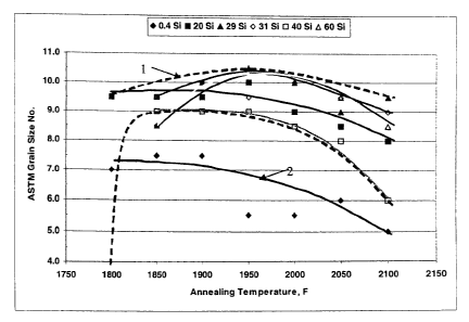
Fig. 1 is a graph showing the relationship of ASTM grain size with annealing
temperatures for niobium sheets with varying silicon content;
Fig. 2 shows micrographs of niobium sheets with varying silicon content;
Fig. 3 shows micrographs of niobium sheets with varying silicon content;
CA 02524430 2005-10-21
P083G6 - 3 -
Fig. 4 shows micrographs of niobium sheets with varying silicon content;
Fig. 5 shows micrographs of niobium sheets with varying silicon content;
Fig. 6 shows micrographs of niobium sheets with varying silicon content;
Fig. 7 shows micrographs of niobium sheets with varying silicon content;
S Fig. 8 shows micrographs of niobium sheets with varying silicon content;
Fig. 9 is a graph showing the relationship of recrystallization with annealing
temperature of niobium sheets with varying silicon content;
Fig. 10 is a graph showing the effect of annealing temperature and silicon
content
on cup depth; and
Fig. 1 I is a graph showing the effect of annealing temperature and silicon
content
on Vickers Hardness.
DETAILED DESCRIPTION OF THE INVENTION
Other than in the operating examples, or where otherwise indicated, all
numbers
or expressions referring to quantities of ingredients, reaction conditions,
etc. used
in the specification and claims are to be understood as modified in all
instances by
the term "about."
The present invention relates to a method for manufacturing niobium or
tantalum
wrought products. The method provides a significant reduction as well as
better
control of the final grain size in niobium or tantalum wrought products. More
particularly, the present invention provides niobium or tantalum wrought
products
that contain greater than S ppm silicon, which has a consistently fme,
uniform, and
fully recrystallized grain structure.
As used herein, the term "wrought products" refers generally to metals that
have
been exposed to thermo-mechanical processing steps to acquire a specific shape
and/or other properties. The thermal steps can include, but are not limited to
annealing, baking, smelting and/or melting. The mechanical steps can include,
but are not limited to working, forging, rolling, upset forging, upset-and-
forge-
CA 02524430 2005-10-21
P08366 - 4
back techniques, hammer forging, drawback forging, flat forging, round
forging,
and radial forging.
Wrought products, as provided in the present invention include, but are not
limited
to generally planar metal forms such as foils (less than about 10 mil in
thickness),
sheets (from about 10 to about 125 mil in thickness), and plates (greater than
about 125 mil in thickness. Other wrought product forms can include tubes,
where a length of metal is hollow in the center (and can have any cross-
sectional
internal and external shape, but often those shapes will be circular, oval,
square,
rectangular, triangular, hexagonal, or octagonal); and rods, which are lengths
of
metal that are solid throughout and can have any cross-sectional internal and
external shape, but often those shapes will be circular, oval, square,
rectangular,
triangular, hexagonal, or octagonal.
In the invention, vacuum arc remelting is used to alloy niobium or tantalum
with
low level silicon additions along with traditional thermo-mechanical
processing
with higher annealing temperatures to produce niobium or tantalum wrought
products with a fine and fully recrystallized grain structure. The inventive
process
provides high yields, a more consistent product, and lower manufacturing
costs.
In an embodiment of the present invention, the silicon is present at a level
of at
least 0.01 ppm, in some cases 0.1 ppm and as high as 60 ppm, in some cases SO
ppm based on the total niobium in the niobium ingot. The amount of silicon in
the
niobium can be any value or can range between any of the values recited above.
In the present method, a blend containing niobium powder and silicon powder is
formed and pressed to form a pressed blend. As used herein, the term "pressed
blend" refers to a solid form where a mixture of materials are compressed to
form
a stable shape, which is capable of being attached to another body, such that
when
the other body melts, the pressed blend melts and commingles with the elements
of the other body.
CA 02524430 2005-10-21
P083GG - S -
The pressed blends are attached to electrodes that contain niobium or tantalum
using a suitable method and both are melted under vacuum arc remelting (VAR)
conditions and subsequently cooled. In other words, the niobium or tantalum
acts
as an electrode, and is melted by striking an arc between a charged electrode
and
the niobium or tantalum, under vacuum. The arc power can be from 2S to SOV
and from 7,000 to 10,000 amps.
Typically, a pressed blend of niobium and silicon is used with a niobium
electrode
and a blend of tantalum and silicon is used with a tantalum electrode.
The melted electrode and pressed blend is cooled to form an alloy ingot.
Thenno-mechanical processing steps as indicated above are applied to the alloy
ingot to form a wrought product as described above.
After forging, the alloy ingot can be vacuum annealed at a temperature of at
least
950°C and up to 1150°C. The annealing temperature for the
wrought product can
be any value or range between the values recited above.
The annealing step can take at least 5 minutes and up to 180 minutes. The
length
of time for annealing can be any value or can range between any values recited
above.
2S The annealing step can result in at least 7S% recrystallization and in some
cases
up to at least 9S% recrystallization.
In an embodiment of the invention, sequential rolling and annealing steps can
be
carried out on the alloy ingot. Any suitable combination of rolling and
annealing
steps can be used. In a particular embodiment of the invention, the following
steps are used:
CA 02524430 2005-10-21
P083GG - 6
I) rolling the wrought product to an intermediate thickness;
II) annealing the wrought product of I) at a temperature of
from 950 to 1150°C for a period of from 30 minutes to 180
minutes;
III) rolling the wrought product of II); and
IV) annealing the wrought product of III) at a temperature of
from 950 to 1150°C for a period of from 30 minutes to 180
minutes and then cooling the wrought product to room
temperature.
In an embodiment of the invention, the intermediate thickness I) can be from
0.5
to 2 cm and the wrought product III) can have a thickness of from 0.005 to
0.24
cm.
A particular embodiment of the invention provides a method of making a silicon-
containing alloy of niobium or tantalum by
a) melting niobium or tantalum to form a melt;
b) adding 0.1 to 60 ppm of silicon, based on the niobium or
tantalum in the melt;
c) cooling the melt to form an alloy ingot;
d) applying thermo-mechanical processing steps to the alloy
ingot to form a wrought product.
The thermo-mechanical processing steps in d) can include i) forging the alloy
ingot to form a wrought product; and ii) annealing the wrought product at a
temperature of from 950 to 11 SO°C.
Particular sequential rolling and annealing steps can be used in this
particular
embodiment as described above. The annealing steps can result in at least 75%
recrystallization and in some cases up to at least 95% recrystallization.
CA 02524430 2005-10-21
P08366 - 7 -
In an alternative embodiment, scrap niobium or tantalum is consolidated via
VAR,
ISM, or other cold hearth melting techniques and a silicon addition made
directly
to the melt or via the VAR process described above.
In the present invention, the cooled, annealed plate and sheet has a fine and
uniform ASTM grain size up to 10, and can be as coarse as 5. In an embodiment
of the invention, the ASTM grain size is in the range of 8 to 10.
The present invention also provides for wrought product made according to the
above described processes, where the wrought products are selected from a
foil, a
sheet, a plate, a tube, and a rod.
The present invention also provides for deep drawn cups or sputtering targets
obtained using, made from, or including the above-described wrought products.
The present invention will further be described by reference to the following
examples. The following examples are merely illustrative of the invention and
are
not intended to be limiting. Unless otherwise indicated, all percentages are
by
weight.
Examples
Niobium ingot were obtained that contained approximately 0.57 ppm Si, 5.3 ppm
Mo, 1200 ppm Ta, other minor (less than 1 ppm) impurities with the balance
being
niobium.
Pressed blends of Niobium/silicon powders were prepared and attached to each
respective electrode. The electrodes and pressed blends were melted under
vacuum
arc remelting conditions under argon atmosphere and cooled to form an ingot.
The ingots were then forged to sheet bar and rolled to 0.030 inches (0.076 cm)
thick sheet and annealed at 1950°F (1066°C) for 90 minutes. This
sheet was then
CA 02524430 2005-10-21
P08366 - 8 -
rolled to 0.010 inches (0.025 cm) thick and individual samples were annealed
according
to one of
the following
conditions:
(i) 1800F (982C) for 90 minutes,
(ii) 1850F (1010C) for 90 minutes,
(iii) 1900F (1038C) for 90 minutes,
(iv) 1950F ( 1066C) for 90 minutes,
(v) 2000F (1093C) for 90 minutes,
(vi) 2050F (1121C) for 90 minutes,
and
(vii) 2100F (1149C) for 90 minutes.
The following table shows the results from Glow Discharge Mass Spectrometry
(GDMS) and Inductively Coupled Plasma Mass Spectrometry (ICP) analyses
from surface samples of niobium ingots. The results for the GDMS analyses only
1 S include those elements that, in at least one sample, had a concentration
above
detectability limits. V.AR processing of the electrodes neither substantially
increased nor decreased the concentrations of the elements listed in the
table.
CA 02524430 2005-10-21
Pos3~~ - 9 -
GDMS ~ Results for Metallic Elements
Ingot ID Nb1 Nb6 Nb5 Nb2 Nb4 Nb3
Ingot Si 0 30 40 50 60 70
Add'n, ppm
Finallngot 0 10 20 30 40 50
Si, ppm
Si 0.40 20 31 29 40 60
B 0.02 0.05 0.09 0.03 0.09 0.05
Na 0.02 <0.01 <0.01 0.03 <0.01 <0.01
AI 0.07 0.07 0.05 0.09 0.15 0.08
P 0.37 0.75 0.75 2.1 0.52 1.9
S 0.53 0.01 0.05 0.92 0.05 0.53
CI <0.01 <0.01 0.05 <0.01 <0.01 <0.01
Ti 0.08 0.05 0.07 0.06 0.04 0.03
V 0.02 0.04 0.02 0.02 0.02 0.01
Cr 0.03 0.07 0.05 0.05 0.05 0.03
Mn <0.005 1.1 <0.005 <0.005 <0.005 <0.005
Fe 0.15 0.05 0.49 0.42 0.27 0.51
Co <0.001 0.01 0.03 0.002 <0.001 <0.001
Ni 0.005 0.04 0.01 0.02 0.009 0.02
Cu <0.01 <0.01 0.02 <0.01 0.02 0.05
Y <0.001 0.003 0.003 <0.001 <0.001 0.005
Zr 0.21 0.19 0.19 0.21 0.15 0.22
Nb bal. bal. bal. bal. bai. bal.
Mo 4.5 4.3 4.5 4.3 3.8 3.7
Hf 0.03 0.02 0.02 0.04 <0.01 0.02
Ta <=1000 <=1000 <=1000 <=1000 <=800 <=1000
W 1.5 3.9 1.5 2.5 1.5 2.5
ICP Results r InterstitialElements
fo
C 5 8 8 4 5 7
N 6 4 8 12 9 4
O 33 28 31 58 33 42
-
_ ~
_
Glow Discharge Mass Spectrometry
Experience has indicated that an ASTM grain size of 8 or finer (as determined
by
ASTM Test Method E 112) with at least 90% recrystallization (determined by
visual inspection) almost completely eliminates flatness and surface finish
issues.
Figure 1 shows the results of the microstructural characterization of the
niobium
CA 02524430 2005-10-21
P08366 - 10
sheet samples. The legend in this and other figures shows the silicon content
(ppm) of the sheet. The dashed lines (for example the line labeled 1 ) in
Figure 1
indicates the band of ASTM grain sizes for all the silicon modified samples
independent of silicon content. Figures 2-8 show micrographs of the sheet
samples. The micrographs were taken at a magnification of 100x. The samples
were annealed as indicated below:
Figure 2: I 800F (982C) for 90
minutes
Figure 3: 1850F (1010C) for 90
minutes
Figure 4: 1900F (1038C) for 90
minutes
Figure 5: 1950F (1066C) for 90
minutes
Figure 6: 2000F (1093C) for 90
minutes
Figure 7: 2050F (1121C) for 90
minutes
Figure 8: 2100F (1 I49C) for 90
minutes
I S Previous research had shown there was considerable variation in the grain
size
(i.e., ASTM 4 to l 0) of niobium sheet manufactured using prior art methods
without silicon additions. Figure I shows that without any silicon addition
(see
line 2) the finest grain size achieved was ASTM 7.5, which is only marginally
acceptable for deep draw applications. With one exception (i.e., 20 ppm Si),
greater than 90% recrystallization of the silicon modified sheet was not
possible
using the prior art production cycles. Consequently, grain sizes could not be
determined. On the other hand, ASTM grain sizes of 8.5 or finer were
consistently produced in niobium sheet containing silicon additions using
annealing cycles 50°F (28°C) hotter than that those used in
prior art production
cycles. However grain coarsening began to occur at annealing temperatures of
approximately 2000°F (1093°C). Grain sizes of ASTM 9.0 or finer
were
consistently produced in all silicon modified sheet samples using annealing
temperatures between 1900°F (1038°C) and 2000°F
(1093°C) with an optimum
annealing temperature of 1950°F ( 1066°C).
As the silicon content increases, annealing temperatures need to increase to
fully
recrystallize a sheet. Figure 9 shows this trend (a dashed line indicates the
90%
recrystallization target). Using the prior art production cycles, grain size
CA 02524430 2005-10-21
P08366 - 11 -
measurements could only be performed on sheet samples with less than 20 ppm
Si. Only at temperatures above 1900°F {1038°C) was full
recrystallization of all
of the silicon modified niobium sheet possible.
Not wishing to be bound to a single theory, it is believed, based on the
results, that
the silicon combines with niobium to form Nb3Si; and/or NbSi2 particles in the
niobium or possibly with oxygen to produce sub-micron size Si02. Rolling (cold
working) to sheet produces a uniform dispersion of these particles that on
subsequent annealing act initially as grain nucleation sites and, with
continued
annealing, as grain boundary pinning points.
Figure 10 effect of annealing temperature and silicon content on Cup Depth,
determined using the Olsen Ductility test (QM-1-1823). The dashed lines in
Figure
10 indicate the band of cup depths for all the silicon modified samples
independent of silicon content. The dotted lines indicate the range (~16) of
cup
depth measurements for 0.005 inch sheet from the prior art described above.
The
results clearly show that silicon modified niobium sheet has at least as good,
if not
slightly better, drawability than prior art niobium sheet. Additionally, the
silicon
modified niobium sheet maintains its drawability over almost the entire anneal
temperature range evaluated, the exception being when the sheet is annealed
using
the prior art production cycle. This is also consistent with the effect of
impurities
on grain size and recrystallization as discussed above. Poorer
recrystallization
will reduce the ability of the niobium sheet to withstand large amounts of
deformation. Consequently, the measured cup depth will be reduced.
Figure 11 shows effect of annealing temperature and Silicon Content
on Vickers Hardness, determined using an automated Vickers Hardness Tester.
The dashed lines in Figure 11 indicate the band of hardness measurements for
all
the silicon modified samples independent of silicon content. The dotted lines
indicate the range (~la) of hardness measurements for 0.005" sheet from the
prior
art methods described above. If the data from the sheet annealed at
1800°F is
CA 02524430 2005-10-21
P0836G - 12 -
ignored because it was not fully recrystallized, then the hardness numbers for
the
silicon modified sheet fall within the upper half of the band from the
previous
work. This suggests that while on average the silicon modified sheet may be
slightly harder than prior art sheet, it is still within the range typically
seen for this
material and has less variation.
Increasing the annealing temperature at all silicon contents has essentially
no
effect on the VHN.
Although the invention has been described in detail in the foregoing for the
purpose
of illustration, it is to be understood that such detail is solely for that
purpose and that
variations can be made therein by those skilled in the art without departing
from the
spirit and scope of the invention except as it may be limited by the claims.