Note: Descriptions are shown in the official language in which they were submitted.
CA 02524673 2005-11-03
-1 -
METHOD FOR MOUNTfNG AN ELECTRONIC COMPONENT ON A SUBSTRATE
This invention relates to an assembly process of an electronic component on an
insulating support called a substrate that includes a plurality of conductive
tracks.
This process can be applied during the manufacturing of transponders in the
form of
a card or an electronic label which thickness is generally low.
Electronic label is understood to mean an assembly comprising at least one
insulating support, an antenna and an electronic component, usually a chip.
The card
or electronic label made using the process according to the invention is found
in
numerous applications as a mean of identification, control or payment.
The subject of this invention is particularly focused on the assembly of at
least one
electronic component on the substrate of a thin card or label. An electronic
component is an element such as: a chip, a capacity, a resistance, a diode, a
fuse, a
battery, a display, or also an assembly comprising a coated chip provided with
contact areas.
Cards or labels are known by those skilled in the art where components are
mounted
on a substrate, on which conductive tracks and connection areas (usually in
copper)
are engraved. The components are usually bonded, then their contacts are
welded
onto the tracks or onto the conductive connection areas of the substrate. The
electric
contact between the connection areas of the component and those of the
substrate
is achieved by means such as: bonding with a conductive glue, welding by means
of
ultrasounds, welding by means of a hot applied tin-based alloy.
Cards are also known that are provided with components whose contacts are
provided with claws or spikes (bumps) which are embedded by pressing into the
engraved connection areas of the substrate. The document W00055808 describes
the production of a connection between a chip and the contact areas of an
antenna
by hot lamination. The contacts of the chip include bumps that are embedded in
the
conductive material of the antenna's connection area producing a deformation
in
these areas.
CA 02524673 2005-11-03
-2-
The connections of components on substrate conductors can also be obtained by
means of conductive wires welded on one hand on a substrate conductor and on
the
other hand on a conductive area of the component.
In order to protect the components and the circuits wired in this way, an
epoxy resin
can be cast on all or part of the substrate surface in order to coat the
circuit
components assembly. According to another embodiment, an insulating sheet is
laminated on all or part of the substrate that cons the component or
components and
the conductive tracks in the vicinity.
The document EP0786357 describes a contactless card that comprises a chip
mounted on a substrate and connected to an antenna coil placed on the edge of
the
substrate. The chip is placed in a substrate zone located on the exterior of
the loop
formed by the antenna coil in the vicinity of one of the edges of the card.
This off-
center position of the chip protects the latter against stresses caused by
bending of
the card. The connection of the antenna coil to the chip is carried out by hot
pressing the bumps of the chip contacts on the end tracks of the coil.
According to a
variant this connection is achieved by soldering of wires ("wire-bonding")
between the
chip contacts and the tracks deriving from the coil.
The document US2002/0110955 describes a manufacturing method of an electronic
module comprising a substrate and at least one chip. The latter is either
glued on
one of the substrate faces, or hot pressed inside the substrate thickness in
order to
be level with the surface. Furthermore, the substrate includes conductive
areas to
which the chip is connected by means of conductive tracks made by silk-
screening,
according to a preferred variant. The chip contacts include bumps on which
tracks,
thus applied, end up to con the bumps. A final step consists in applying a
thin film or
a protection lacquer on the chip and on the conductive tracks located near the
chip.
The transponders whose components are assembled according to the known
processes described above present a disadvantage at the level of quality and
reliability of the connection between the component and conductors, In fact,
this
connection can be interrupted totally or intermittently due to mechanical
stresses
applied to the transponder during its use. More particularly, the thin
transponders
such as cards or electronic labels are easily deformable by flexion or
twisting. These
CA 02524673 2005-11-03
-3-
stresses can appear during the normal application of the transponder such as
for
example on a label that is applied on the surface of an object presenting
protrusions.
Despite the protection of the components by coating or lamination of an
insulating
film, the connections of the components are subjected to internal traction and
compression causing their breakage when the transponder is deformed. This
phenomenon is further increased during repetitive deformations leading to the
strain
of the connection that will finally break after a few flexions or torsions
suffered by the
transponder.
The aim of this invention is to avoid the drawbacks described above, namely to
increase reliability and quality of the electric connection between the
electronic
component or components and the substrate conductive tracks while reducing the
manufacturing costs of the transponder.
The aim of this invention is also to offer a manufacturing process for this
type of
transponder in the form of a card or a label that is capable of resisting
flexions or
twisting without interrupting component connections.
These aims are achieved by an assembly process of at least one electronic
component including sensibly flat conductive areas that are connected to
conductive
tracks placed on the surface of a generally flat insulating support, called
substrate,
comprising the following steps:
- placing the substrate on a work surface, the face including conductive
tracks
being oriented upwards,
- placing the electronic component into a cavity of the substrate situated in
a
zone including the conductive tracks, the conductive areas of the electronic
component coming into contact with the corresponding tracks of the substrate,
- applying a layer of insulating material which extends at the same time on
the
electronic component and at least on a substrate zone surrounding said
component,
said process is characterized in that the contact between the conductive areas
of the
electronic component and the conductive tracks of the substrate realizes an
electric
connection ensured by the pressure of application of the insulating material
layer on
the electronic component.
CA 02524673 2005-11-03
-4-
The electronic component also called the electronic module is usually formed
by a
chip whose contacts located on one of its faces are set off on a conductive
film,
called "lead frame" constituting contact areas that extend the small
dimensions of the
chip contacts. In one embodiment example, the opposite face of the chip is
coated
by an insulating material that is usually epoxy resin. The "lead frame" allows
the
facilitation of the connection of the electronic module on the conductive
tracks of a
printed circuit. The majority of semi-conductive components mounted on the
surface
of printed circuits include such "lead frames".
The conductive tracks of the substrate are defined in an extensive way. They
can be
made up of pads or conductive areas connected to the conductive segments of a
circuit engraved chemically or deposited by silk-screening on the substrate.
For
example, this type of circuit can constitute the antenna of a contactless card
that
serves to supply energy to the card and exchange digital data by means of a
terminal.
It is important to note that the method according to the~invention does not
require any
welding, nor any kind of anchoring of component contacts on the circuit
conductors.
It is thus sufficient for the contact surfaces of component and substrate to
have been
pressed one against the other by presenting approximately flat surfaces. The
component is retained on the substrate by the insulating material covering the
latter
by extending on its periphery.
The cavity in the substrate is used to maintain temporarily the component
between
its placing step and the depositing of the insulating layer. This cavity can
be carried
out by means of different ways such as milling or cutting a window by
stamping, or
simply through the deformation of the substrate by heating the component
during its
placing on the substrate.
The advantage of mounting the component according to this method resides in
the
fact that the contact between the component and the circuit conductor is
maintained
when the transponder is bent or twisted. In fact, the internal forces
appearing at the
level of connection tend to make the contacts slide one on the other without
producing any breakage as in the case of a welded or anchored connection.
Repeated stresses exerted an the transponder cause a "self-cleaning" effect on
the
CA 02524673 2005-11-03
-5_
conductors by rubbing their surfaces together. Therefore, the performance of
the
connection as well as its reliability and its electric conductivity are
greatly improved.
The invention will be better understood thanks to the following detailed
description
that refers to the enclosed drawings given as a non-limitative example, in
which:
- Figure 1 represents a component in the form of an electronic module provided
with contact areas.
- Figure 2 represents an overview of a thin transponder comprising a substrate
and a component provided with contact areas protected by an insulating layer
- Figure 3 shows an enlarged section of a the transponder in Figure 2
according
to the axis A-A
- Figure 4 shows a section of a transponder assembly comprising two
substrates and one component provided with contact areas
- Figure 5 shows a section of a transponder assembly comprising two
substrates and one component made up of a chip inserted in one of the
substrates.
The component (1 ) in Figure 1 forming an electronic module includes a chip
(2)
protected by coating (4) in insulating material such as an epoxy resin. The
chip
contacts are connected to contact areas (3) formed inside a tinned copper
conductive sheet, for example, forming the "lead frame".
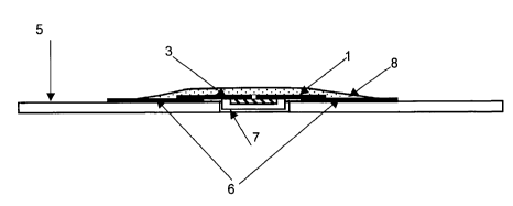
Figure 2 and the section according to the illustrated axis A-A in Figure 3
show an
example of a transponder that includes a thin substrate (5) that can be
deformed on
which the component (1 ) in Figure 1 is placed. The upper surface of said
substrate
includes tracks or conductive areas (6) engraved, glued or printed by silk-
screening,
for example. The coated part (4) of the component (1 ) is inserted into a
cavity (7)
made up of milling or a window cut into the substrate in order to minimize the
final
thickness of the transponder. The conductive tracks (6) of the substrate are
in
contact with the component conductive areas (3) only by means of pressure
without
using welding or conductive glue. The approximately flat surfaces in contact
in this
way do not include any particular type of relief serving as an anchorage
point. The
maintenance of the component on the substrate and the pressure on its contacts
are
CA 02524673 2005-11-03
. -6-
assured by an insulating layer (8) extended at the same time on the visible
surface of
component and on a substrate zone in the vicinity of the component. According
to a
variant, this insulating Payer can be extended on the whole upper surface of
the
substrate.
A transponder achieved in this way can be deformed without any interruption of
component connections on the substrate conductors. The contact areas of the
"lead
frame" will have a tendency to rub on the substrate tracks under the action of
internal
forces produced by the transponder deformation. .
Figure 4 shows a variant of the transponder assembly according to the
invention
method, where the coated part (4) of the component (1 ) is inserted into a
cavity or
located in a window of a first insulating substrate (5). The conductive areas
(3) of the
component are thus arranged on the Power surface of the substrate (5). A
second
substrate (9) that includes, on its upper surface, a plurality of conductive
tracks such
as for example an antenna (6') and contact tracks (6) situated facing those of
the
component is applied on the first substrate (5). The assembly of two
substrates (5, 9)
is carried out by gluing or by hot or a cold lamination according to the
arrows L. The
electric contact of the component with the tracks (6) of the second substrate
is
achieved by means of the lamination or gluing pressure. The final thickness of
the
transponder is limited to that of the two superimposed substrates (5, 9).
According to another variant, the component (1 ) does not include a coating,
the chip
(2) is thus directly protected by the first substrate (5). The chip is either
inserted into
a cavity (7) that is pre-worked into the substrate, or hot pressed into the
substrate
material in such a way that the contact areas (3) of the component (1 ) are
applied
against the inner surface of substrate (5).
The direct insertion of the component into the substrate material without a
pre-
worked cavity is carried out by heating the chip during its placing that leads
to the
local softening and a deformation of the substrate. The chip is then pressed
into the
substrate by means of an adapted tooling to the desired depth. The cavity
constituted in this way is adapted to the chip outline and maintains the
position of the
chip or the component assembly during the lamination of the second substrate.
CA 02524673 2005-11-03
_7_
The second substrate (9) is assembled in the same way as in the previous
variant.
The thickness of the first substrate (5) can in this way be reduced to a value
closer to
that of the chip.
Figure 5 represents a variant of the transponder assembly where the component
is
made up by the chip (2) alone, free of "lead frame". In this case, as in the
previous
one, the chip (2) is either housed in a pre-worked cavity or pressed into the
material
of the first substrate (5) in such a way as to make its contact surfaces (3')
appear on
the substrate surface (5) level. The second substrate (9) is provided with
conductive
tracks (6) facing those of the chip intended for its connection by means of
the
pressure of gluing or lamination of the assembly of the two substrates (5, 9).
The
contact surfaces (3') of the chip (2) are of course flat allowing their
friction on the
corresponding conductive tracks of the second substrate in case of the
transponder
deformation.
The insulating layer deposited on the component and on all or part of the
surface of
the substrate as well as on the second substrate laminated onto the first
substrate
can include a decoration or a marking on the external surface characterizing
the final
transponder. The first substrate can furthermore also include decoration on
the
opposite side to that supporting the conductive tracks.
The method according to the invention is also applied to the assembly of cards
called
"dual" that is to say comprising on one hand a set of flat contacts showing on
the
level of one of the external faces of the card and on the other hand an
internal
antenna in the form of a set of conductive tracks. This contacts set is placed
on one
of the faces of a module and each contact is linked to a conductive area on
the
opposite side of the module. The latter is inserted into a cavity provided
with a
window cut into a first substrate whose thickness is approximately equal to
that of the
module. The contacts set shows on the surface level of the substrate
constituting the
external face of the card and the conductive areas of the opposite side lean
against
the conductive tracks of a second substrate assembled on the first substrate.
A chip or a supplementary electronic module as previously described,
completing this
assembly, can be mounted on either of the substrates. The conductive areas of
this
CA 02524673 2005-11-03
_ $ _
module are connected by pressure on the corresponding conductive tracks of the
surface of one of the substrates.
It is also possible to assemble and then laminate more than two superimposed
substrates comprising conductive tracks and the electronic modules whose
conductive areas are connected by the lamination pressure to the corresponding
conductive tracks arranged on the faces of either of the substrates.