Note: Descriptions are shown in the official language in which they were submitted.
CA 02525620 2005-11-10
WO 2005/025001 PCT/US2004/023358
1
EMBEDDED RF VERTICAL INTERCONNECT FOR
FLEXIBLE CONFORMAL ANTENNA
BACKGROUND
(0001) Typical active array architectures include one or more ferrite
circulators for passive duplexing and control of scattering in
microwave antennae. These circulators are passive "discrete"
microwave devices, which may include, e.g., a microstrip/stripline
resonator circuit on a ferrite substrate that is sandwiched between a
magnet and magnetic carrier plate.
(0002) For a conformal panel architecture, the active devices
comprising the T/R modules can be mounted on the back of the
panel. The circulators are situated between the radiating apertures
and T/R modules. There exists a need to be able to bury these
microwave devices, e.g., circulators and other microwave devices,
e.g., integrated circuits comprising switches, filters and MEMs, while
realizing the vertical transitions to interconnect the devices to
the other components within the antenna, e.g.,
Transmit/Receive modules (T/R modules) and radiators. Burying
microwave circulators and other discrete microwave devices poses
a challenge.
CA 02525620 2009-09-16
2
SUMMARY OF THE DISCLOSURE
(0003) An RF signal transition comprises a channelized microstrip
transmission structure, and a coplanar wave guide structure in
electrical communication with the channelized microstrip transmission
structure. A caged troughline transition structure is in electrical
communication with the coplanar wave guide structure. A caged
coaxial transmission structure is in electrical communication with the
troughline transition structure. The signal transition may be embedded
in a flexible printed wiring board structure with a circulator for a
conformal antenna structure.
(0003a) Accordingly, in one aspect of the present invention there is
provided an antenna system comprising:
a radiator layer assembly comprising a plurality of
radiators;
a circulator layer having a plurality of circulators each in
electrical communication with a corresponding one of said plurality
of radiators;
a plurality of transmit/receive (T/R) modules each
having an input port and an output port in electrical
communication with a corresponding port of one of said
circulators; and
an RF feed layer having an input/output (I/O) port
and a plurality of T/R module ports each connected to a
respective one of said T/R modules,
wherein said radiator layer assembly and said circulator
layer are fabricated in a laminated multi-layer structure including a
printed wiring board (PWB) structure, said plurality of circulators
embedded within spaces defined in said PWB structure.
CA 02525620 2009-09-16
2a
BRIEF DESCRIPTION OF THE DRAWINGS
(0004) Features and advantages of the disclosure will readily be
appreciated by persons skilled in the art from the following detailed
description when read in conjunction with the drawing wherein:
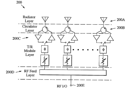
(0005) FIG. 1 is a functional block diagram of an embodiment of
an active array which can be fabricated in accordance with aspects
of the invention.
(0006) FIG. 2 shows an exploded perspective view of a
conformal antenna assembly including a multi-layered conformal RF
transition structure according to an embodiment of the present
invention.
(0007) FIG. 2A is a simplified schematic cutaway of a portion of the
RF transition portion of FIG. 2.
CA 02525620 2005-11-10
WO 2005/025001 PCT/US2004/023358
3
(0008) FIG. 3A shows a cross-sectional partially exploded schematic
view of a first portion of an embodiment of the present invention
shown;
(0009) FIG. 3B shows a schematic cross-sectional view of a second
portion of the embodiment of the present invention;
(0010) FIG. 3C shows an exploded schematic cross-sectional view of
the embodiment of the present invention shown in FIGS. 3A and 3B;
(0011) FIG. 4 shows a top schematic representation of a portion of a
microstrip connecting the circulator to a vertical RF transition
according to an embodiment of the present invention.
(0012) FIGS. 5A and 5B show, respectively, a top view and a cross-
sectional view along lines 5B, of a schematic representation of a
portion of a microstrip connecting the circulator to a vertical RF
transition according to an embodiment of the present invention.
(0013) FIGS. 5C and 5D show, respectively, a top view and a cross-
sectional view along lines 5D, of a schematic representation of
another portion of the microstrip connecting the circulator to a
vertical RF transition according to an embodiment of the present
invention.
(0014) FIGS. 6A and 6B show respectively a top view and a cross-
sectional view along the lines 6B, of a caged troughline transition line
contained within the PWB 16 according to an embodiment of the
present invention.
CA 02525620 2005-11-10
WO 2005/025001 PCT/US2004/023358
4
(0015) FIGS. 7B and 7A show respectively atop view and a cross-
sectional view along the lines 7B, of a caged coaxial transition line
contained within the balun layer according to an embodiment of the
present invention.
DETAILED DESCRIPTION OF THE DISCLOSURE
(0016) In the following detailed description and in the several figures
of the drawing, like elements are identified with like reference
numerals.
(0017) FIG. 1 is a schematic block diagram of an exemplary
embodiment of a active array system 200 which can be implemented
in accordance with aspects of this invention. In a general sense, the
array includes a radiator layer 200A, a circulator layer 200B, a T/R
module layer 2000, and an RF feed layer 200D, with an RF
input/output (I/O) port 200E. The T/R module layer includes for each
circulator in the layer 200B a phase shifter and an attenuator, as well
as a receive amplifier and a transmit amplifier connected to ports of
the circulator through a T/R switch. Structures of the array system can
be implemented in multiple layers to provide a conformal
radiating aperture.
(0018) Turning now to FIG. 2 there is shown an exploded perspective
view of a conformal antenna assembly including a multi-layered
conformal RF transition structure 10 according to an embodiment of
the present invention. The conformal antenna also includes an
aperture structure 11 and a backplate 13 between which the RF
transition structure 10 may be sandwiched. To conform to the curved
nature of the antenna aperture, the structure 10 comprises, in an
CA 02525620 2005-11-10
WO 2005/025001 PCT/US2004/023358
exemplary embodiment, a flexible, curved multilayered conformal
antenna RF transition structure,
(0019) Innovations include a new combination of transmission line
structures used in this transition, and lamination processes utilized in
creating three dimensional microwave transmission lines structures in
the flexible sections, e.g., section 12.
(0020) FIG. 2A shows a schematic, cutaway view of a lower portion
of the transition structure 10. A microstrip circulator 44 is mounted into
the flexible multi-layered lower section 12 of the structure 10 in a
generally rectangular opening 70 that is formed in section 12 as
explained in more detail below, The cavity air pockets 46 may also
be machined into selected layers of section 12 prior to a lamination
process, also as described below. Gold wires or ribbon bonds 74 are
used to connect corresponding microstrip traces to and from the
circulator 44 to and from the microstrip traces 42, 80 on the top
surface of the section 12.
(0021) FIG. 2A shows a schematic representation of the positioning
of an RF vertical transition 90 through a laminated multilayer flexible
printed wiring board (PWB) 12 and the balun and radiating aperture
assembly 60. The interconnect 90 interconnects the microstrip
conductor 80 connected to the circulator 44, to the upper layer
assembly 60. The vertical RF transition 90 can include several
microwave transmission line structures 80, 150, 110, 120 to reshape the
electromagnetic field configuration of the RF signal
from the microstrip 80 connected to circulator 44 to that of a "caged"
coaxial transmission line structure as the RF signal enters the layer
assembly 60. There is also a microstrip to vertical caged coaxial
CA 02525620 2005-11-10
WO 2005/025001 PCT/US2004/023358
6
transmission structure 40 for connecting the T/R module to the
circulator. In this view only one structure 40 is illustrated; however it will
be understood that two structures 40 are provided for each circulator
to provide the transmit or receive connection between the T/R
module and the circulator as shown in FIG. 1.
(0022) It will be appreciated that the exemplary embodiment of the
antenna of FIG. 1 is adapted for transmit and receive operations, and
so it will be understood that generally the "input" and "output" ports
of various circuits can also be used as "outputs" and "inputs" unless
otherwise apparent from the circuits.
(0023) FIG. 3A shows a cross-sectional schematic view of a portion
of the PWB 12 comprising a lower portion of the structure 10. An RF
transmit receive interface module 30 is connected to the PWB 12, and
may include a flip chip assembly or chip-scale package including an
IC flip chip 203 having a ball-grid 201 including solder balls 202
respectively aligned with many of the catchpads 16e in the laminate
12. The IC chip 203 integrates functions of a T/R module in this
exemplary embodiment. The module 30 is electrically connected to
the structure 10 through solder ball connections to the catchpads.
The module 30 allows RF and DC signals to be connected to the PWB.
(0024) FIG. 3B shows in cross section the upper portion 60 of the
structure 10 which is assembled to the portion 12. The upper portion
60 comprises a balun layer 62 and a radiator assembly layer 64. The
balun layer 62 may be formed of a lower dielectric balun layer 66
and an upper dielectric balun layer 67 sandwiched between a lower
metal layer 60b and an upper metal layer 60c. The lower metal layer
60b forms a ground plane, and has formed therein a cutaway 60f
CA 02525620 2005-11-10
WO 2005/025001 PCT/US2004/023358
7
within which may be formed a catchpad 60e formed to connect
the vertical transition line 102 (FIG. 3A) with the coaxial vertical
transition 120. The lower balun layer 66 may also have a via and
catchpad forming a portion of a groundplane interconnect 122. The
lower balun layer 66 may also have formed thereon a signal
transmission strip conductor pattern formed in a metalization layer 66g
formed on the upper surface of the lower balun layer 66. The upper
balun layer 67 may have formed on its upper surface the metalization
layer 60c which forms a groundplane, and has cut in it a clearout 60f
through which passes a vertical coaxial signal transition 120a.
(0025) The radiator layer 64 includes a dielectric layer 64a which has
embedded therein a radiator conductor pattern defining a plurality
of radiators, including exemplary radiator 94, which is electrically
connected to the vertical transition 120a. The radiator assembly layer
64 has formed therein, as shown in FIG. 3B, a via 96 for connection
with the vertical coaxial transition 120a through a clearout 60f in the
upper metal layer 60c of the balun layer 62. A dielectric radome
layer 76 covers the top surface of layer 64a.
(0026) The balun and radiator layer assembly 60 may be attached
to an upper metal layer 28g (FIG. 3A) of an upper dielectric laminate
28 of the PWB 12 by an adhesive layer 68. The layer 68 may contain a
layer 68a of bondply adhesive having formed in it vias 68b filled with
conductive ink for electrical connection through the adhesive layer
68, e.g., between the catchpad 60e at the lower end of the signal
transition line 120 and the catchpad 28e at the upper end of the
trough line 102, or between the groundplane 28g on the upper
surface of the laminate 28 and the groundplane formed by the
metalization layer 60b on the bottom of the laminated layer 60. This
CA 02525620 2005-11-10
WO 2005/025001 PCT/US2004/023358
8
can provide a connection to a ground plane interconnection 122
connecting the groundplane 60b on the bottom surface of the balun
layer 66 with the groundplane 60c on the upper surface of the balun
layer 67. In this exemplary embodiment, the balun layer 62 is formed
of the two balun layers 66, 67 for ease of forming the metalization 66g'
on the upper surface of the lower balun layer 66 for forming a
horizontal signal transition pattern 66g thereon.
(0027) The adhesive layer 68 in this exemplary embodiment may be
a Z-axis adhesive which electrically connects the catchpads 60e (in
the lower metal layer 60b of the balun layer 66) and 28e (connected
to the upper end of the trough line 102), and also the respective
ground planes 60b and 28g. The Z axis adhesive, e.g., a layer of 3M
7373 or 3M 9703 manufactured by 3M, in the regions of the catchpads
60e, 28e and ground-planes 60b and 28g will be squeezed together,
and in the areas of the clearouts 60f and 28f. Therefore, the randomly
distributed conductive particles contained in the Z-axis adhesive will
form an anisotropic vertical electric connection between the
catchpad 60e and the catchpad 28e and between the ground
planes 60b and 28g, while not shorting the vertical transitions 102, 120
to the respective ground planes 60b and 28g in the region of the
clearouts 60f and 28f. This allows the flexible DC/RF manifold
assembly 12 to be electrically attached to the upper balun and
radiating layers 60, 62 as that assembly is formed of increasing
curvature. Such connections are suitable for DC and microwave
frequencies, e.g., across a planar and curved surface interface,
assuming that the section 12 is more relatively planar, i.e., less curved,
than the balun/radiator section 6. The balun/radiator section 60 may
be a part of the structure of the aperture structure 11, e.g. an
embedded dipole aperture structure.
CA 02525620 2005-11-10
WO 2005/025001 PCT/US2004/023358
9
(0028) This use of Z-axis adhesive may be substituted for some or all
of the other adhesive layers 18, 22 and 26, e.g. to accommodate
further flexibility of the section 12.
(0029) Turning now to FIG. 3C, there is shown an exploded cross-
sectional view of the exemplary multilayered conformal PWB
assembly 12 which serves as an RF/DC feed section in this
embodiment. In an exemplary embodiment, the PWB 12 includes
sections 14 and 15. The section 14 may be made up of a lower
dielectric laminate 16 and an upper dielectric laminate 20.
(0030) The lower dielectric laminate 16 may be of about 6 mils in
thickness and may include a lower dielectric layer 16a of about 2 mils
in thickness, which may be made of Kapton (TM), which may be
sandwiched between a lower metal layer 16b and an upper metal
layer 16c, each of which may be etched to form, e.g., catchpads
16e, clearouts 16f, and ground/signal plane 16g. These dimensions
are for an exemplary embodiment. The dielectric layer 16a may itself
be formed with pre-cut or pre-drilled via openings 16h that may be
filled with conductive ink as is known in the art to connect, e.g., a
catchpad 16e in the lower metal layer 16b to a ground/signal plane
16g in the upper metal layer 16c.
(0031) Above the lower dielectric laminate 16 may be a lower
adhesive layer 18, which may be on the order of about 3 mils thick.
The lower adhesive layer 18 may comprise a layer of bondply
adhesive 18a, which may be predrilled or precut to form via openings
18b filled with conductive ink for connecting, e.g., catchpads 16e
and/or ground/signal planes 16g in the upper metal layer 16c of the
lower dielectric laminate 16 through the lower adhesive layer 18.
CA 02525620 2005-11-10
WO 2005/025001 PCT/US2004/023358
The adhesive layer 18 may also have cut into it a portion of the
opening 70 that will be formed when the layers 16, 18, 20, 22 and 24
are laminated together.
(0032) Above the lower adhesive layer 18 may be an upper
dielectric laminate 20, which may be of about 6 mils in thickness and
may include an upper dielectric layer 20a of about 2 mils in thickness,
which may be made of Kapton GM), which may be sandwiched
between a lower metal layer 20b and an upper metal layer 20c,
each of which may be etched to form, e.g., catchpads 20e,
clearouts 20f, and ground/signal planes 20g. The dielectric layer 20a
may itself be formed with pre-cut or pre-drilled via openings 20h
that may be filled with conductive ink as is known in the art to
connect, e.g., a catchpad 20e in the lower metal layer 20b to a
ground/signal plane 20g in the upper metal layer 20c. The upper
dielectric layer 20a may also have cut into it a portion of the opening
70 that will be formed when the layers 16, 18, 20, 22 and 24 are
laminated together.
(0033) Above the upper dielectric laminate 20 may be a middle
adhesive layer 22, which may be on the order of about 3 mils thick.
The middle adhesive layer 22 may comprise a layer of bondply
adhesive 22a, which may be predrilled or precut to form via openings
22b filled with conductive ink for connecting, e.g., catchpads 20e
and/or ground/signal planes 20g in the upper metal layer 20c of the
upper dielectric laminate 20 through the middle adhesive layer 22.
The adhesive layer 20 may also have cut into it a portion of the
opening 70 that will be formed when the layers 16, 18, 20, 22 and 24
are laminated together.
CA 02525620 2005-11-10
WO 2005/025001 PCT/US2004/023358
11
(0034) Above the middle adhesive layer 22 may be the upper
section 15 of the multilayered laminate section 12. The upper section
15 may include a lower dielectric laminate 24, which may be on the
order of about 10 mils thick. The lower dielectric laminate 24 may be
fabricated of a dielectric layer 24a, such as Duroid (TM), sandwiched
between a lower metal layer 24b and an upper metal layer 24c,
each of which may be etched to form, e.g., catchpads 24e,
clearouts 24f, and ground/signal planes 24g. The lower dielectric
layer 24a may itself be formed with pre-cut or pre-drilled via openings
24h that may be filled with conductive ink as is known in the art to
connect, e.g., a catchpad 24e in the lower metal layer 24b to a
ground/signal plane 24g in the upper metal layer 24c. The lower
dielectric laminate 24 may also have cut into it a portion of the
opening 70 that will be formed when the layers 16, 18, 20, 22 and 24
are laminated together.
(0035) Above the lower dielectric laminate 24 may be formed an
upper adhesive layer 26, which may be on the order of about 3 mils
thick. The upper adhesive layer 26 may comprise a layer of bondply
adhesive 26a, which may be predrilled or precut to form via openings
26b filled with conductive ink for connecting, e.g., catchpads 24e
and/or ground/signal planes 24g in the upper metal layer 24c of the
lower dielectric laminate 24 through the upper adhesive layer 26. The
upper adhesive layer 26 may also have cut into it a portion of the
opening 70 that will be formed when the layers 16, 18, 20, 22 and 24
are laminated together.
(0036) Above the upper adhesive layer 26 may be formed an upper
dielectric laminate 28, which may be on the order of about 60 mils
thick. The upper dielectric layer 28 may be formed of a dielectric
CA 02525620 2005-11-10
WO 2005/025001 PCT/US2004/023358
12
layer 28a, e.g. a Duroid (fM) layer, sandwiched between a lower
metal layer 28b and an upper metal layer 28c, each of which may be
etched to form, e.g., catchpads 28e, clearouts 28f, and ground/signal
planes 28g. The upper dielectric layer 28a may be formed with pre-
cut or pre-drilled via openings 28h that may be filled with conductive
ink to connect, e.g., a catchpad 28e in the lower metal layer 28b to a
catchpad 28e in the upper metal layer 28c, e.g., as part of transition
102. The upper dielectric laminate 28 may also have cut into it
opening 46.
(0037) When laminated together, as shown in FIG. 3A, the respective
catchpads 16e, 20e, 26e and 28e along with respective ground/signal
planes 16g, 20g, 24g and 28g may form, e.g., ground plane
interconnection path 32 or an RF vertical signal transition 40, e.g.,
between the T/R module 30 and the buried RF feed microstrip 42
formed by a portion of the upper metal layer 28c of the upper
dielectric laminate 28 as shown in FIG. 4.
(0038) The buried microstrip circulator 44 (FIG. 3A) may comprise a
permanent magnet 50 which is atop the buried microstrip circulator
circuitry formed in a layer of metalization 54 formed on top of a ferrite
layer 56, which in turn is on a steel carrier 57 connected to a portion of
a ground plane 16g formed in the metal layer l6c of the laminate 16
by a layer 58 of conductive epoxy. The permanent magnet 50 is
separated from the circulator layer 54 by a dielectric spacer 52. The
circulator 44 may be connected to the buried RF feed microstrip 42
by wire or gold ribbon 74.
(0039) The structure 10 can be formed as a curved, conformal
structure, as illustrated in FIG. 2.
CA 02525620 2005-11-10
WO 2005/025001 PCT/US2004/023358
13
(0040) FIG. 4 shows a top schematic representation of a portion of
the microstrip conductor 80. The microstrip conductor 80 has a
contact pad 82 at one end thereof, and is fabricated on a top
surface of the lower laminate 24. Conductor filled plated vias 85 (FIG.
3A) are formed along the periphery of each air pocket cavity 46 and
surrounding transition 102 as explained in more detail below. The
plated vias 85 also serve to form groundplane interconnects 96 (FIG.
4) to create a virtual sidewall for the cavities 46, sufficient for creating
an RF shielded cavity 46 necessary for RF transmission line structures.
(0041) As shown in FIG. 4, the region of the cavity 46 in the direction
of arrow A contains the microstrip conductor 80 with an air dielectric
over the microstrip conductor. In the region of the cavity 46 in the
direction of arrow B the microstrip contact pad 82 passes through
clearout 28f extending toward the catchpad 28e on the lower end of
the vertical transition 102 and the contact pad 82 is contacted by the
catchpad 28e. In this region the conductor trace may be covered
with a dielectric, e.g. comprising laminate 28. The location of the
transition marked by arrows A and B is also shown in FIG. 2A.
(0042) FIGS. 5A and 5B show, respectively, a top view and a cross-
sectional view, taken along lines 5B-5B in FIG. 5A, of a schematic
representation of a portion of the microstrip trace 80, comprising a
channelized microstrip transmission structure 81 at area 5A (FIG. 2A),
interconnecting the gold wire or ribbon bond 74 from the circulator 44
to the contact pad 82 (FIG. 4), at area 5B (FIG. 2A). Side walls of the
opening 46 have formed therein conductive vias 96 to define a
metallized channel. Field lines 86 depict the shape of the electric
field for the channelized transmission structure.
CA 02525620 2005-11-10
WO 2005/025001 PCT/US2004/023358
14
(0043) FIGS 5C and 5D show, respectively, a top view and a cross-
sectional view taken along lines 5D-5D of FIG. 5C, of a schematic
representation of another transmission structure 150 interconnecting
the gold wire or ribbon bond 74 from the circulator 44 to the contact
pad 82. The location of 5D is shown also in FIG. 2A. The channelized
microstrip 81 transitions to the channelized, conductor backed,
dielectric filled, coplanar waveguide (CPW) transmission structure 150,
since the ground planes 24G close in on the conductor strip 80,
resulting in reshaping of the electromagnetic fields. Thus, the gap 84
between the microstrip conductor 80 and the ground conductors 24g
is tapered from the spacing at the junction between the structures 81
and 150 to a smaller gap size at the vertical transmission structure 100
(FIG. 6A).
(0044) FIGS. 6A and 6B show respectively a top view and a cross-
sectional view along lines 6B-6B of a caged troughline transition line
structure 100 formed in laminate layer 28. The location of 6B is also
shown in FIG. 2A.
(0045) FIGS. 7B and 7A, respectively, show a top view and a cross-
sectional view along lines 7B-7B, of a caged coaxial transition line 120
contained within the lower balun layer 66 and upper balun layer 64 of
the balun layer 60.
(0046) As shown in FIGS. 5A, 5B, 5C and 5D, the channelized
microstrip 81 field configuration within the area of cavity 46 transitions
to a channelized conductor backed CPW transmission structure 150.
The channelized conductor-backed coplanar waveguide 150 may
be formed of the channel or gap 84 tapering from the input of the
CPW 150 to the output. The gap dimensions of the channelized
CA 02525620 2005-11-10
WO 2005/025001 PCT/US2004/023358
microstrip structure 81, as indicated in FIG. 5A remain essentially
constant as gaps 84 between the ground planes 24g formed in the
upper metalization layer 24c of the lower laminate 24 and the
microstrip conductor 80. As shown in FIG. 5B the field lines 86 in this
region of the air cavity 46 are generally between the microstrip 80
and the groundplane 24g formed in the lower metalization layer 24b
of the lower laminate 24. These field lines pass through the dielectric
24a of the lower laminate 24. As shown in FIG. 5C, the channels 84
are narrowed toward vertical transition 102, while maintaining a
suitable resistance, e.g., 50 ohm impedance. At the same time the E-
field 86 concentrates more across the gaps 84 and less along a
bottom groundplane 24g through the dielectric 24a on which the
microstrip 80 is formed. This redistribution of the E-fields 86 across the
gaps 84 continues, so that the E-fields are shaped to be essentially
parallel to the plane of the microstrip conductor 80 in order to allow
the RF signal to transition to the caged troughline 102 (FIG. 6B) to
realize a matched vertical transition with minimal discontinuity. The
caged troughline 102 then transitions to a caged coaxial 120 as the RF
signal enters the balun layer 60 as described in more detail below.
(0047) As shown in FIG. 6A, a caged troughline transition 100 is
formed by a vertical signal transition post 102 extending vertically
through the upper laminate 28 from the contact pad 82 of the
microstrip 80 at the terminus of the tapered regions of the gap 84
where the E-fields have been rendered essentially horizontal.
Surrounding the post 102 are a plurality of generally evenly spaced
apart posts 104a-104g. The posts 104a-104g are arranged in generally
a circular pattern surrounding the post 102 as shown in FIG. 6B with an
opening 106 in the pattern to allow for interconnection to the most
tapered end of the CPW structure 150 as shown in FIG. 5C and FIG.
CA 02525620 2005-11-10
WO 2005/025001 PCT/US2004/023358
16
5D. The upper ends of the posts 104a-g are in electrical contact with
an intervening ground plane 60b of the balun/radiator laminate 60.
The posts 104a-104g surrounding the pin in the 0.060" thick layer 28a
can be formed in vias in the upper laminate 28, The grounded posts
104a-104g are an approximation to a continuous conducting wall
forming a grounded shield for transition post 102, which minimizes
leakage into the surrounding layers. The grounded posts 104a-104g
are also a means to keep the shape of the signal e-field lines 86
transitioning vertically along the post 102 generally horizontal as
shown in FIG. 6B.
(0048) FIGS. 7A and 7B illustrate a caged coaxial vertical transition
119 which includes a vertical post 120, which is connected to post 102
across an adhesive layer 68 by via 68b connecting catchpads 28e
and 60. Posts 122a-122h form generally a closed equally spaced
circular pattern around the post 120, providing an outer shield for the
center conductor post 102. The E-fields 86 transition vertically along
the posts 122a-h generally as was the case for posts 102a-102g,
maintaining a horizontal orientation from the post 120 to the posts
122a-h, the posts 122a-102h also serving to shield the post 120 and
prevent signal leakage into the surrounding layer.
(0049) At high frequencies (5 - 15 GHz), there may be a mismatch
between the caged troughline transmission line 100 and microstrip line
81. To account for this, an embodiment of the invention implements a
microstrip matching circuit to obtain better impedance matching for
the transition. To obtain a better match, a two-section matching
topology is implemented on the microstrip line 80, which can be
represented by an inductive and a capacitive element, As shown in
FIG. 4, a narrowed discontinuity 83 in the microstrip conductor 80
CA 02525620 2005-11-10
WO 2005/025001 PCT/US2004/023358
17
serves to form an inductive element and the discontinuity from the air
dielectric in the cavity 46 and the dielectric 28a dielectric forms the
capacitive element.
(0050) Important to realizing the microwave transmission line
structures within a buried multi-layer flexible PWB is the fabrication of
blind and buried vias interconnects between the layer of the
laminates. FIG. 3A shows the RF feed 40 to the circulator 44, by way of
vias structures in the adhesive layers 18 and 22 and the laminates 16
and 20, along with the catchpads 16e and 20e with laminates 16 and
20.
(0051) In conventional PWB fabrication, catch pads are required to
facilitate the plating into the via holes. Often complex sequential
plating and lamination processes have been used to create blind
and buried vias and catchpads. Also the introduction of openings 70
and air cavity pockets 46 add a factor that prohibits using
conventional lamination processes. Two novel and simplified
lamination processes may be utilized for making buried microwave
signal and ground interconnects as employed in embodiments of the
present invention. Depending on the application, either one or a
combination of both of these two novel methods can be used for the
novel construction of new microwave vertical interconnects across a
large area of multilayer flexible laminates of section 12 according to
embodiments of the present invention, The first method is a
colamination process and the second method utilizes anisotropically
conductive Z-axis adhesives.
(0052) In the colamination process, the pattern of vias 16h, 20h, 24h,
28h, 18b, 22b and 26b can be predrilled into each of the laminate
layers 16, 20 and 24 and each of the bondply layers 18, 22 and 26.
CA 02525620 2005-11-10
WO 2005/025001 PCT/US2004/023358
18
The via holes 16h, 20h, 24h, 28h, 18h, 22h and 26h can then be filled
with any of a variety of suitable conductive metal inks or epoxies, e.g.,
such as transcent liquid phase scintering ("TLPS"), manufactured by
Ormer Circuits, Inc., or a copper paste called ALIVH ("any layer
interstitial via hole) marketed by Matsushita. The via holes 16h, 20h,
24h, 28h, 18b, 22b and 26b constituting layered pairs are filled with
material(s) prior to lamination, and the adhesive bondply layers 18, 22,
26 are then assembled and laminated together. The conductive inks
create an interconnect between the catchpads, e.g., 16e on
laminate 16 and 20e on laminate 20 thus realizing the microwave via
structures for the embodiment of the present invention. This process is
known in the art but has not been used for forming signal transitions
through a flexible printed wiring board laminate, e.g., for mixed signal
or microwave applications. Test results have shown functionality of
the RF interconnect up to 13 GHz for a multilayer assembly in one
exemplary embodiment.
(0053) The second method uses anisotropically conductive Z-axis
adhesive films ("ZAF") such as those noted above, as an adhesive to
realize the interconnections between the laminates, e.g., 16, 20, 24, 28
and 60. ZAF is an adhesive film filled with conductive particles that
allow interconnections between layered pairs through the adhesive
thickness (the "Z-axis"). The conductive particles are spaced far
enough apart for the ZAF to be electrically insulating in the plane of
the adhesive film. Similar to colamination, ZAF can be used in a
conventional lamination process to realize RF and DC interconnects
of multiple layers with only one or two operations. Unlike colamination,
the interconnects realized by ZAF are indiscriminate and thus the
layered pairs e.g. 14 may require additional patterned features such
as catchpads and/or ground planes and clearouts. The ZAF
CA 02525620 2005-11-10
WO 2005/025001 PCT/US2004/023358
19
intermediate paired catchpads and ground planes, are compressed
together enough to create a conductive path between the
respective features through the more densely compressed
conductive particles. In the region of a clearout(s) this compression,
does not occur and the Z-axis adhesive remains dielectric. Test results
have shown the functionality of the RF interconnect up to 16 GHz for a
multilayer assembly.
(0054) Although the foregoing has been a description and
illustration of specific embodiments of the invention, various
modifications and changes thereto can be made by persons skilled in
the art without departing from the scope and spirit of the invention as
defined by the following claims.