Note: Descriptions are shown in the official language in which they were submitted.
CA 02525621 2005-11-10
WO 2005/018226 PCT/US2004/025164
SYSTEM AND METHOD FOR PROCESSING
AND DISPLAYING LIGHT ENERGY
TECHNICAL FIELD OF THE INVENTION
[0001] This invention relates in general to the field of optical imaging and
more particularly to a system and method for processing and displaying light
energy.
1
CA 02525621 2009-08-04
WO 2005/018226 PCT(US20041025164
BACKGROUND OF THE INVENTION
[0002] Optical imaging has become increasingly important in today's
society. One area associated with optical imaging relates to the processing of
light
energy using various architectures, such as array devices, imaging components,
or
sensing elements for example. These architectures may generally include a
light sensing
configuration that generates a stream of sensor data. The stream of sensor
data may then
be processed and transmitted for display at a suitable next location. There
are numerous
problems and deficiencies associated with this scenario. For example, large
amounts of
processing time and power may be needed to execute this process. This may
result in
latency problems, bandwidth limitations, or an inhibition in resolution
performance. In
addition, systems capable of such operations may be cumbersome, as well as
difficult to
position and manipulate. Accordingly, the ability to provide an architecture
capable of
processing sensor data efficiently and effectively, while occupying minimal
space,
presents a significant problem for system designers in the field of optical
imaging.
2
CA 02525621 2005-11-10
WO 2005/018226 PCT/US2004/025164
SUMMARY OF THE INVENTION
[0003] From the foregoing, it may be appreciated by those skilled in the
art that a need has arisen for an improved sensor data processing approach
that offers
suitable processing of information in an optical imaging environment. In
accordance
with, one embodiment of the present invention, a system and method for
processing and
displaying light energy are provided that substantially eliminate or greatly
reduce
disadvantages and problems associated with conventional sensor data
acquisition and
processing techniques.
[0004] According to one embodiment of the present invention, there is
provided a method for processing and displaying light energy that includes
receiving a
plurality of photons reflected by an object and generating sensor data that is
based on the
plurality of photons received. The sensor data is processed in order to
generate
processed sensor data. A segment of the processed sensor data that directly
corresponds
to the plurality of photons is displayed such that the segment may be viewed.
[0005] Certain embodiments of the present invention may provide a
number of technical advantages. For example, according to one embodiment of
the
present invention, a processing approach is provided that occupies minimal
space. This
is a result of the integration of several components that may be grown (or
manufactured)
individually, layer by layer, or that may be constructed as a single integral
unit. The
architecture provided by the teachings of the present invention allows a
single integral
unit to receive light radiation, to translate the light radiation into
electronic data, and then
to properly display the data in a suitable format at a suitable next location.
[0006] Another technical advantage associated with one embodiment of
the present invention relates to the reduced power needed to operate the
architecture.
This is a result of the direct transmission of processed sensor data to a
display pixel or to
a small number of display pixels. For example, a sensing element may be used
to
receive incoming light and generate sensor data, which is digitally processed.
The
processed sensor data may then be directly transmitted to a specific display
pixel. This
3
CA 02525621 2005-11-10
WO 2005/018226 PCT/US2004/025164
configuration may eliminate processing power that would otherwise be needed to
execute an imaging task covering a broad area of imaging information. Certain
embodiments of the present invention may enjoy some, all, or none of these
advantages.
Other technical advantages may be readily apparent to one skilled in the art
from the
following figures, description, and claims.
4
CA 02525621 2005-11-10
WO 2005/018226 PCT/US2004/025164
BRIEF DESCRIPTION OF THE DRAWINGS
[0007] To provide a more complete understanding of the present
invention and features and advantages thereof, reference is made to the
following
description, taken in conjunction with the accompanying figures, wherein like
reference
numerals represent like parts, in which:
[0008] FIGURE 1 is a simplified block diagram of one embodiment of a
system for processing and displaying sensor data in an optical imaging
environment;
[0009] FIGURE 2 is a simplified block diagram of an example
implementation of the system of FIGURE 1; and
[0010] FIGURE 3 is a flowchart illustrating a series of example steps
associated with a method for processing and displaying sensor data in an
optical imaging
environment.
CA 02525621 2005-11-10
WO 2005/018226 PCT/US2004/025164
DETAILED DESCRIPTION OF THE EXAMPLE EMBODIMENTS
[0011 ]FIGURE 1 is a simplified block diagram of a system 10 for
processing and displaying sensor data in an optical imaging environment.
System 10
may be provided in any environment that seeks to display an optical image such
that it
may be adequately viewed at a next location. Alternatively, system 10 may be
positioned in any suitable infrared environment that seeks to detect infrared
energy in
order to display light radiation levels associated with any suitable picture,
pattern, image,
object, or element. Thus, system 10 may be provided in any spectral range that
provides
some distinguishing characteristics (based on heat, energy, or any other
infrared, light, or
optical parameter) that may be used in order to properly display infrared data
or
information.
[0012] System 10 includes a sensor element 12 and a sensor drive 16.
Sensor element 12 may collect sensor data based on a portion of photons being
reflected
by (or otherwise associated with) an object 14. The photons may be directed or
communicated toward sensor element 12 such that light radiation may be
properly
received and suitably processed by sensor element 12. System 10 may also
include
support electronics 20, a display drive 22, and a display element 26. In
addition, system
may optionally include a thermal stabilization element 30 that maintains a
temperature gradient across one or more elements coupled thereto.
[0013] According to the teachings of one embodiment of the present
invention, system 10 operates to provide an architecture that properly
processes and
displays infrared data received by sensor element 12. Sensor element 12 may
detect
incoming light and generate infrared data that is digitally processed. System
10 may
digitally process the sensor data received from object 14 such that electronic
values are
correlated to radiation levels associated with object 14.
[0014] The processed sensor data may be transmitted to a specific
location within display element 26. The processed sensor data may be
transmitted
directly to display element 26 or directly to a small number of display
elements or pixels.
6
CA 02525621 2005-11-10
WO 2005/018226 PCT/US2004/025164
This allows a minimal amount of processing power and time because each digital
logic
unit is operating to process the specific sensor data received from a single
unit within
sensor element 12. This allows spectrum shifting to be achieved by
manipulating an
input spectrum to a visible spectrum range using a single integral unit to
focus optical
energy onto a specific location.
[0015] System 10 may also execute sensor data processing on a pixel by
pixel basis. Each pixel may be independent and self-supporting and, thereby,
each pixel
does not need information from its neighbors in order to achieve its intended
function.
Accordingly, the electronics needed to drive each pixel may be contained
locally as each
pixel achieves its own processing that may be used in displaying radiation
levels
associated with object 14 at display element 26. Intermediate processing
layers may also
be provided (as illustrated in FIGURE 1) in order to assist in this operation
or to execute
more advanced processing operations. For example, analog and digital
processing may
be effectuated in order to achieve pixel by pixel processing and display.
[0016] Sensor element 12 is a light radiation sensing device that operates
to receive photons or light radiation reflecting by object 14. Sensor element
12 may
alternatively be any suitable sensing device, component, tool, or element
operable to
collect or otherwise receive (actively or passively) any data associated with
light energy,
heat, or radiation levels. For example, sensor element 12 may comprise a pixel
or
multiple pixels used in the reception of infrared data that serves as a basis
for displaying
object 14. Sensor element 12 may be coupled to sensor drive 16 and share one
or more
processing operations with sensor drive 16. Each of the pixels may communicate
with
each other in order to reach a consensus concerning uniformity corrections.
This
operation may be accomplished in cooperation with support electronics 20.
[0017] Sensor drive 16 is coupled to support electronics 20 directly or via
thermal stabilization element 30 and operates to process sensor data received
from sensor
element 12. Sensor drive 16 may include sense amplifiers and/or equalizers
operable to
effectuate this task. Sensor drive 16 may properly receive sensor data and
process the
information such that it is communicated to support electronics 20 to be
formatted or
7
CA 02525621 2005-11-10
WO 2005/018226 PCT/US2004/025164
otherwise further processed for display. One or more of the operations of
sensor drive
16 may be incorporated into the architecture of sensor element 12 or support
electronics
20, or alternatively any one or more of these elements may be combined to form
a single
functional unit having the capabilities as described above.
[0018] Support electronics 20 includes circuitry (inclusive of any suitable
hardware or software where appropriate) that operates to facilitate the
coupling between
one or more sensing elements (e.g. pixels included within sensor element 12)
and
display element 26. Support electronics 20 is coupled to display drive 22.
Support
electronics 20 may also include a memory element used to execute calibration
operations, to eliminate non-uniformity characteristics, or to effectuate any
other suitable
operations in accordance with particular needs. Support electronics 20 may
include
elements used for image processing of the sensor data received from sensor
drive 16.
The image processing may include analog or digital processing and inclusive of
distributed circuitry processing where appropriate. The capabilities of
support
electronics 20 may also be inclusive of more sophisticated non-linear analog
processing
operations. Support electronics 20 may be a dedicated configuration for a
single pixel
column or, alternatively, configured to be dedicated for an entire array of
elements where
appropriate.
[0019] Display drive 22 and display element 26 cooperate in order to
display information based on light radiation associated with object 14.
Display drive 22
may receive information that is suitably processed by support electronics 20
and
communicate this information to display element 26 such that it may be viewed.
Alternatively, display element 26 may be replaced with additional processing
elements
or such processing elements may be positioned between display drive 22 and
display
element 26 in accordance with particular needs. Additionally, display drive 22
and
display element 26 may be provided as a single integral element, where
appropriate, that
operates to receive a selected amount of processed sensor data and to display
that
information appropriately. Display element 26 may be associated with organic
light
emitting diode (OLED), liquid crystal on silicon (LCOS), or reflective liquid
crystal
display (LCD) technologies. Alternatively, display element 26 may be
associated with
8
CA 02525621 2005-11-10
WO 2005/018226 PCT/US2004/025164
any other suitable technology operable to properly display processed infrared
information.
[0020] In an alternative embodiment of the present invention, thermal
stabilization element 30 may be provided to system 10. In certain
applications, such as
when implementing a configuration with vanadium oxide, longwave elements, or
other
appropriate architectures, cooling may be needed in order to balance the
temperature of
the pixels and to produce a uniform temperature gradient across sensor drive
16.
Accordingly, thermal stabilization element 30 may be provided to offer a layer
that
stabilizes or cools infrared sensors (or other suitable visible sensors) .
Thermal
stabilization element 30 may also provide noise reduction capabilities for a
corresponding device or component.
[0021] The elements of system 10 may be implemented in any suitable
hardware, software, object, device, component, or element. In one embodiment
of the
present invention, system 10 may be grown layer by layer using a number of
suitable
manufacturing processes. Alternatively, system 10 may be grown in different
layers and
bonded together in some integration phase. Additionally, system 10 may be
grown as a
single element using appropriate semiconductor processing techniques.
Moreover, any
one of more of the elements of FIGURE 1 may be combined into one or more
integral
pieces having the functions and capabilities used in the processing and the
display of
light energy associated with object 14.
[0022] A significant reduction in latency may be achieved as a result of
the architecture of system 10. `Latency' generally refers to the time interval
that is
necessary for a photon, which impinges on the input of sensor element 12, to
propagate
through the associated configuration, to be suitably processed, and then to be
adequately
displayed at display element 26. In particular, latency may create significant
problems
for overlay fusion devices and image intensifiers, to which minimal latency
periods are
critical. The architecture of the present invention allows latency values to
be minimized
to the nano-second range. Additionally, latency issues may be addressed while
achieving a full-field integration rather than a rolling integration. For
example, such a
9
CA 02525621 2005-11-10
WO 2005/018226 PCT/US2004/025164
full-field application may involve implementing system 10 in conjunction with
snapshots
or output video where an array element may be placed in a layer that is
actually
performing the digital correction or digital readout functions.
[0023] System 10 may also achieve enhanced resolution characteristics.
The enhanced resolution is due to one or more bandwidth limiting parameters
being
eliminated from the corresponding architecture of system 10. Thus, because of
the pixel
by pixel architecture of system 10, bandwidth allocations may be optimized,
which
allows for a higher resolution of object 14 to be displayed at display element
26.
[0024] It should also be appreciated that numerous other systems may be
involved in the operation of the elements of FIGURE 1. A complete system or
multiple
subsystems (inclusive of additional electronics and appropriate interfaces)
may be
provided in conjunction with these elements in order to effectuate suitable
processing of
infrared energy associated with object 14. Additional elements may also be
added to
system 10 in order to properly format the sensor data in a manner that allows
suitable
viewing by an end user. Additional electronics may also be involved in the
decoding of
information being provided to system 10.
[0025] In operation of an example embodiment, system 10 may use pixel
by pixel processing in order to provide a single pass-through device for
displaying
infrared data. Each given pixel provided in sensor element 12 may include, for
example,
a 1:1 direct coupling or connection to a given output or to a set of
designated locations
within display element 26. Accordingly, one pixel on the output may be
directly
correlated to one pixel on the input of system 10. This configuration may
avoid
problems associated with an array of pixels. System 10 allows data to be
formatted in a
way that allows an end user to view or to suitably process the incoming sensor
data on a
pixel by pixel basis.
[0026] System 10 may offer a processing approach that occupies minimal
space. This may be the result of the integration of several components that
may be
grown or manufactured individually (layer by layer) or that may be constructed
as a
CA 02525621 2005-11-10
WO 2005/018226 PCT/US2004/025164
single integral unit. The architecture provided allows a single integral unit
to receive
light radiation, to translate the light radiation into electronic data, and
then to properly
display the data in a suitable format at a next location.
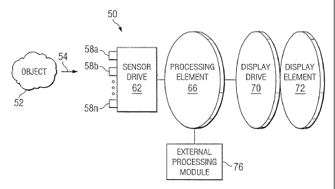
[00271 FIGURE 2 is a simplified block diagram of an example
implementation of system 10. FIGURE 2 illustrates an architecture 50 that may
be
provided within any tool, device, component, element, or object that receives
infrared
energy and seeks to display that energy for viewing by an end user. In
general, an
example object 52 may project, direct, reflect or otherwise be associated with
photons,
radiation, or light energy in a direction as indicated by an arrow 54. The
light energy
may be received by a number of pixels 58a-n that are coupled to sensor drive
62 of
architecture 50. Architecture 50 also includes a processing element 66 that is
coupled to
an optional external processing module 76. A display drive 70 and a display
element 72
may also be provided to architecture 50 in order to receive sensor data and
properly
display the sensor data such that it may be viewed.
[00281 Pixels 58a-n are sensor elements that may be provided in order to
detect or otherwise receive photons, radiation, or light energy to be
correlated to analog
signals reflecting infrared energy. Pixels 58a-n may comprise any suitable
material such
as lead (Pb) salt or vanadium oxide for example. Pixels 58a-n may receive
light energy
and properly process, format, or otherwise direct the sensor data to sensor
drive 62. In
an example embodiment, sensor drive 62 executes signal conditioning for each
pixel
58a-n. Sensor drive 62 receives the sensor data and communicates the sensor
data to
processing element 66.
[00291 Processing element 66 is an object used to receive and properly
process sensor data based on photons reflected by object 52. In an example
embodiment,
processing element 66 may include a complimentary metal oxide semiconductor
(CMOS) layer operable to execute designated processing on sensor data received
from
sensor drive 62. Processing element 66 may include memory cells that depend on
external stimuli for controlling system temperature parameters that may be
properly
varied. This may allow each pixel 58a-n to be adjusted based on a selected
calibration
11
CA 02525621 2005-11-10
WO 2005/018226 PCT/US2004/025164
procedure. Additionally, a thermal stabilization element may be provided in
conjunction
with processing element 66 such that a consistent temperature gradient is
maintained
across the interface between sensor drive 62 and processing element 66. The
thermal
stabilization element may behave similar to thermal stabilization element 30
described
above with reference to FIGURE 1.
[0030] Processing element 66 may execute analog or digital processing
(or any combination thereof) in order to suitably process sensor data. In
addition,
processing element 66 may be inclusive of any suitable device operable to
provide or to
assist in the processing of sensor data. For example, processing element 66
may include
a field programmable gate array (FPGA) operable to program non-uniformity
corrections. In addition, processing element 66 may include other suitable
processing
elements such as an erasable programmable read-only memory (EPROM), an
electrically
erasable read-only memory (EEROM), an application specific integrated circuit
(ASIC),
a microprocessor, or any other integrated circuit or processing element
operable to
provide some processing or manipulation of sensor data received from sensor
drive 62.
These elements may also be provided external to processing element 66, for
example,
within external processing module 76. Processing element 66 may also execute
distributed computing or be confined to pixel by pixel configurations.
Processing
element 66 may also execute situational or dynamic programming, allowing
processing
to be immediately impacted in accordance with current system needs.
[0031] Processing element 66 may also receive one or more instructions
from external processing module 76. External processing module 76 may also be
inclusive of any of the elements described above with reference to processing
element
66. External processing module 76 may communicate with processing element 66
in
order to offer an external programming agent in providing processing tasks to
be
executed by processing element 66. Alternatively, any of the operations or
capabilities
of processing element 66 may be provided in external processing module 76
using any
suitable combination such that these elements collectively process incoming
sensor data
appropriately.
12
CA 02525621 2005-11-10
WO 2005/018226 PCT/US2004/025164
[0032] Display drive 70 and display element 72 operate in a similar
fashion as described above with reference to FIGURE 1 and display drive 22 and
display
element 26. In an example embodiment, display drive 70 may assist in the
processing of
information received from processing element 66 such that the information is
properly
formatted and suitably directed to display element 72. Display element 72 is
an object
capable of displaying infrared information such that it may be properly viewed
by an end
user.
[0033] FIGURE 3 is a simplified flowchart illustrating a series of
example steps associated with a method for processing and displaying infrared
energy.
FIGURE 3 is described with reference to FIGURE 2 in order to identify example
components that may potentially be used to effectuate the operations being
described.
The description provided has been offered for purposes of example and teaching
only
'and should not be construed to limit the plethora of other environments,
configurations,
architectures, and systems that may benefit from the teachings of the present
invention.
[0034] The method begins at step 100 where object 52 is emitting light
energy (or reflecting photons) as indicated by arrow 54. The light energy may
be
properly focused through accompanying optics to a selected one or more of
pixels 58a-n
at step 102. The optics may be included in any suitable device, component,
tool,
element, or object provided in conjunction with architecture 50 or system 10.
Optics
may operate to focus a `hot spot' associated with object 52 onto selected
pixels 58a-n.
Pixels 58a-n may execute the delivery of information such that sense
amplifiers and
equalizers are invoked at sensor drive 62 in order to properly communicate the
information in evaluating the level of light energy associated with object 52.
Thus, an
analog or a digital value may be received that indicates, on some selected or
designated
range, what is being seen. The optical radiation may be received and then
converted into
an electronic signal at step 104. At step 106, the signal may be suitably
processed and
output into an analog or a digital format. Such an operation may be achieved
by sensor
drive 62 in cooperation with processing element 66 (and optionally external
processing
module 76).
13
CA 02525621 2005-11-10
WO 2005/018226 PCT/US2004/025164
[0035] At step 108, the information may be formatted or otherwise further
processed such that it is received by display drive 70 and properly displayed
by display
element 72. Display element 72 may display the information in any suitable
format at
step 110. For example, display element 72 may display this information using
any
suitable number of pixels. Display element 72 may also display this
information using a
one to one correlation.
[0036] Depending on the sensing element being implemented, uniformity
corrections may also be executed. Memory cells or an analog device may be used
that
maps sensor data to a given pixel, providing some offset or gain (for a given
temperature
or for an input dynamic range) in order to execute some non-uniformity
correction.
Additionally, display drive 70 may include electronics modified to the
calibration for
display element 72, which allows for the correction of bad pixels or non-
uniformities.
Display drive 70 may then output this data to be displayed by display element
72. Where
appropriate, display element 72 may also include an analog to digital
conversion for
providing a digital output for viewing by an end user.
[0037] Some of the steps illustrated in FIGURE 3 may be changed or
deleted where appropriate and additional steps may also be added to the
flowchart.
These changes may be based on specific infrared system architectures or
particular
communications arrangements or configurations and do not depart from the scope
or the
teachings of the present invention.
[0038] Although the prent invention has been described in detail with
reference to particular embodiments, it should be understood that various
other changes,
substitutions, and alterations may be made hereto without departing from the
spirit and
scope of the present invention. For example, although the present invention
has been
described with reference to a particular configuration, the present invention
may be used
in numerous other applications that seek to identify images or elements based
on infrared
energy. For example, system 10 may be used in conjunction with a charge-
coupled
device (CCD) detector, or in inspection applications that seek to identify
designated
pieces of information or data segments. Additionally, system 10 has
applications in
14
CA 02525621 2005-11-10
WO 2005/018226 PCT/US2004/025164
medical devices where images are deciphered and displayed based on their
corresponding light energy levels. Moreover, system 10 may be applied to the
sorting or
qualifying of products. For example, system 10 may be used in conjunction with
mail-
sorting applications where an address (or any other suitable piece of
information) is
sought to be identified.
[0039] In addition, although system 10 has been described as being
constructed in a designated manner, both system 10 and architecture 50 may be
constructed or composed in any suitable fashion. Architecture 50 and system 10
may be
constructed using any appropriate semiconductor techniques. For example,
system 10
and architecture 50 may be grown using semiconductor processes layer by layer
or as an
entire single integral unit. In cases where system 10 or architecture 50 are
grown layer
by layer, these elements may be suitably bonded and then positioned in the
selected
environment. In addition, system 10 and architecture 50 may be constructed and
then
provided in any suitable device, element, object, component, or infrared tool
that seeks to
detect light energy and properly display that information using some display
element.
Moreover, numerous other components may be provided in conjunction with these
elements in order to enhance the processing or display characteristics of the
sensor data
being collected by sensor element 12 or pixels 58a-n. Additionally, various
other
enhancements or modifications may be provided to any of these elements, such
as sensor
element 12 or pixels 58a-n, in order to increase the sophistication or the
capabilities of
the corresponding elements.
[0040] Numerous other changes, substitutions, variations, alterations, and
modifications may be ascertained by those skilled in the art and it is
intended that the
present invention encompass all such changes, substitutions, variations,
alterations, and
modifications as falling within the spirit and scope of the appended claims.
Moreover,
the present invention is not intended to be limited in any way by any
statement in the
specification that is not otherwise reflected in the appended claims.